EP0435752A1 - Breitbandiger Diplexer, besonders für Dekameterwellen - Google Patents
Breitbandiger Diplexer, besonders für Dekameterwellen Download PDFInfo
- Publication number
- EP0435752A1 EP0435752A1 EP90403698A EP90403698A EP0435752A1 EP 0435752 A1 EP0435752 A1 EP 0435752A1 EP 90403698 A EP90403698 A EP 90403698A EP 90403698 A EP90403698 A EP 90403698A EP 0435752 A1 EP0435752 A1 EP 0435752A1
- Authority
- EP
- European Patent Office
- Prior art keywords
- line
- diplexer
- sections
- antenna
- access
- Prior art date
- Legal status (The legal status is an assumption and is not a legal conclusion. Google has not performed a legal analysis and makes no representation as to the accuracy of the status listed.)
- Granted
Links
- 230000008878 coupling Effects 0.000 claims description 2
- 238000010168 coupling process Methods 0.000 claims description 2
- 238000005859 coupling reaction Methods 0.000 claims description 2
- 238000009795 derivation Methods 0.000 claims description 2
- 235000012431 wafers Nutrition 0.000 description 22
- 238000010586 diagram Methods 0.000 description 3
- 238000006073 displacement reaction Methods 0.000 description 2
- 235000012771 pancakes Nutrition 0.000 description 2
- 230000005855 radiation Effects 0.000 description 2
- 230000006978 adaptation Effects 0.000 description 1
- 230000005540 biological transmission Effects 0.000 description 1
- 235000021183 entrée Nutrition 0.000 description 1
- 238000005259 measurement Methods 0.000 description 1
Images
Classifications
-
- H—ELECTRICITY
- H01—ELECTRIC ELEMENTS
- H01P—WAVEGUIDES; RESONATORS, LINES, OR OTHER DEVICES OF THE WAVEGUIDE TYPE
- H01P1/00—Auxiliary devices
- H01P1/20—Frequency-selective devices, e.g. filters
- H01P1/213—Frequency-selective devices, e.g. filters combining or separating two or more different frequencies
Definitions
- the present invention relates to a diplexer for broadband antenna and, in particular, for antenna operating in HF that is to say at frequencies ranging from 3 to 30 MHz.
- the diplexers currently used are designed to perform the diplexing on two given channels at a given frequency in each channel.
- Broadband, "multi-channel" antennas, developed for more than ten years therefore lose much of their interest if they are used with such diplexers.
- the object of the present invention is to avoid this drawback by giving the possibility of using the same diplexer for different transmission frequencies of the two transmitters, which will therefore require the use of a "multi-channel" broadband antenna.
- the subject of the present invention is a diplexer, the length of the line elements of which it is composed is adjustable, as defined by claim 1.
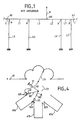
- FIG. 1 is a schematic view showing a diplexer according to the prior art which receives signals at two distinct frequencies F and F ′ respectively on a first and a second access, A1, A2, and delivers them to an antenna A connected to a third access A0.
- F is greater than F ′ so that, in what follows and in claims F and F ′ will be respectively called high frequency and low frequency and the frequencies around F and F ′ will be respectively called high frequencies and low frequencies.
- the access A1 receiving the signal at the frequency F is connected to the access A0 to which the antenna A is connected by a line which two separate connection points M and N separate into three sections of line: a section L connects the point M at access A1, a section L1 connects points M and N and a section L2 connects point N to access AO.
- two sections of line L3, L4, arranged in derivation connect the points M and N respectively to the ground.
- access A2 receiving the signal at frequency F ′ is connected to access AO by a line which two separate connection points M 'and N' separate into three line sections: a section L 'connects point M 'at the access A2, a section L1 ′ connects the points M' and N 'and a section L2 ′ connects the point N ′ to the antenna access, A0; moreover two sections of line L3 ′, L4 ′ connect points M 'and N' respectively to ground.
- the diplexer according to FIG. 1 comprises a diplexer proper constituted by the line sections L2, L4, L2 ′, L4 ′.
- the lengths of these sections are respectively ⁇ ′ / 4, ⁇ ′ / 2, ⁇ / 4, ⁇ / 2, where ⁇ and ⁇ ′ are the wavelengths corresponding to F and F ′; these values are theoretical values but the real values are very close.
- the diplexer according to FIG. 1 also includes two impedance matching circuits constituted respectively by the sections 1L, L3 and L1 ′, L3 ′.
- the introduction, in N ', of the line section L4 ′ leads to a mismatch; to readjust the antenna A with its line L4 ′, to the nominal impedance, it is necessary to place in M ′ the short-circuited line L3 ′.
- the length of the section L3 ′ is very close to that of the section L4′ and therefore of ⁇ / 2; the length of the section L1 ′ depends on the antenna impedance, seen in N ′ and on the line impedance of L2 ′.
- the line section L3 has a length of the order of ⁇ ′ / 2 and the length of L1 depends on the antenna impedance seen from N and the line impedance of L2.
- diplexers corresponding substantially, from the point of view of the lengths of line sections, to the diplexer according to FIG. 1, but in which the line sections L3, L4, L3 ′, L4 ′ are no longer short -circuited by earthing at one of their ends but are open at this end; it is also known to use diplexers in which one of the two channels, for example the low frequency channel, has short-circuited lines while the other channel has open lines.
- a circuit like that of FIG. 1, can only operate with two predetermined values respectively for F and F ′.
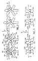
- FIG. 2 shows how the diplexer according to FIG. 1 can be modified to allow it to operate on four distinct values for its low frequency F ′ and four distinct values for its high frequency F.
- the low frequency channel of the diplexer according to FIG. 2 has been provided for ability to couple a transmitter working in the 11, 13, 15 and 17 MHz bands to the antenna while the high frequency channel has been designed to couple a transmitter working in the bands of 13, 15, 17 and 21 to the antenna MHz, which allows the antenna to work in the following pairs of bands: 11-13, 11-15, 11-17, 13-15, 13-17, 13-21, 15-17, 15-21 and 17-21; it should be noted that the pair 11-21 is not used because, the frequency ratio between the two bands being very close to 2, it is difficult to prevent harmonics 2 of the 11 MHz band from disturbing the 21 MHz band.
- the diplexer of FIG. 2 has the same line sections L, L ′, L1, L1 ′, L2, L2 ′, L3, L3 ′, L4, L4 ′, as that of FIG. 1, in a similar arrangement, but the length of the line sections can be modified so that the diplexer can be adjusted according to the frequencies F and F ′ indicated above.
- the low frequency channel that is to say in the channel which conducts the frequency signal F ′ to the antenna A
- the high frequency channel each comprise two switches: C1, C2 for the high channel frequencies, C1 ′, C2′ for the low frequency channel.
- Each switch is a rotary switch with two wafers with four pads per wafer, such as the pads P11 to P14 and P15 to P18 for the first and second wafer of the switch C1; a slider is associated with each wafer, such as the sliders J11 and J12 for the switch C1, which correspond to the wafers carrying the pads P11 to P14 and P15 to P18 respectively.
- the first of the two wafers of each switch has its pads in the connection between the two accesses A1, A2, and the successive pads of each first wafer are interconnected by sections of line; thus the pads P11 to P14 of the switch C1 are in series in this connection, thanks to line sections K11, K12 and K13 which respectively connect the pads P11 and P12, P12 and P13, P13 and P14.
- the second of the two wafers of each switch has its successive pads connected by sections of lines; thus the pads P15 to P18 of the switch C1 are connected by sections K16, K15, K14 disposed respectively between the pads P15 and P16, P16 and P17, P17 and P18.
- the cursor of the first wafer such as the cursor J11 of the switch C1 is connected to one of the two extreme pads of the second wafer while the other end pad and the slider of this wafer are connected to ground.
- the line sections relating to the switch C2, as well as the sliders and the pads of this switch, have been designated in FIG. 2 by adding 10 to the figure of the corresponding element relating to the switch C1, this is how the section K22 of switch C2 corresponds to section K12 of switch C1.
- the line sections of the first wafers that is to say the sections such as K21, which are in series between the accesses A1, A2, have been drawn in the form of rounds while the sections of the second wafers of the switches have been drawn in the form of slots.
- the four cursors of the high frequency channel determine a structure according to FIG. 1, in which the points M and N are the movable ends of the cursors of the first wafers of the switches C1 and C2 and in which the line sections L1, L2, L3, L4 of FIG. 1 are respectively constituted by the sections going from the block P13 to the block P23, from the block P23 to the access AO, from the block P13 to the ground including the section K14, and from stud P23 to ground including the section K24.
- the position occupied by the sliders of switches C1 and C2 is that which is provided when the signal F ′, on port A2, is in the 15 MHz band.
- the diplexer By moving the four sliders of the switches C1 and C2 simultaneously by one pad on the right (in the sense of a displacement in FIG. 2), or by one pad on the left, or by two pads on the left, the diplexer is set for a signal on access A2 whose frequency F ′ is respectively in the band of 17, 13 and 11 MHz.
- switches C1 ′, C2 ′ of the low frequency channel which are identical to those of the high frequency channel and the pads of the wafers of which are wired with line sections of which only the length is different by compared to the high frequency channel.
- the position of the cursors of the low frequency channel corresponds to a working signal, on the access A1, located in the 17 MHz band, while a displacement of all the cursors of the switches C1 ′ and C2′by one pad to the left, or one pad to the right, or two pads to the right would correspond to a working signal, on access A1, located respectively in the bands of 21, 15 and 13 MHz.
- the lengths of the sections are determined by considering a diplexer according to FIG. 1 in which the position of the points M, N, M ′, N 'would be adjustable according to the operating bands and in which the length of the short-circuited sections L3, L4, L3 ′, L4 ′ would also be adjustable.
- the length of the sections such as K11 and K25 can then be determined by simple subtractions taking into account the line lengths which constitute, for example, the cursor J1 of the switch C1 in series with the link going from this cursor to the pad P18 of the second wafer from the same switch.
- the lengths of the line sections between the two switches of the same channel are average lengths determined as a function of the antenna impedance at the average frequency of the frequencies of use.
- FIG. 2 For the sake of simplification, the conductive lines of the various attached figures have been represented by a single line, of course these are symmetrical lines, of the kind of two-wire lines, or asymmetrical, of the kind of coaxial lines.
- FIG. 2 was produced in two-wire lines, which amounts to saying that, to be complete, FIG. 2 should include lines represented by two parallel lines, double cursors with two parallel arms and double pancakes with two superimposed sets of four studs each.
- FIG. 3 is the diagram of an embodiment of a diplexer according to the invention associated with a multi-channel, broadband antenna, A, working in the bands of 13, 15, 17 and 21 MHz.
- this figure which corresponds to Figure 2 but with pancakes with three studs, only the marks relating to the antenna, A, and the access points, AO, A1, A2 have been marked so as not to overload the drawing and allow d '' indicate the lengths in meters of the different line sections.
- the high frequency channel that is to say the one corresponding to access A1
- the low frequency channel has been designed to work in the bands of 13, 15 and 17 MHz.
- the length of the sections in series between the line of access A1 and that of access A2 are respectively 1 -1.6 - 2.16 - 0.5 - 0.8 - 3.46 - 4.21 - 0.56 - 0.7 - 1 - 1.47 meters.
- the four branch line elements they each comprise three sections of line in series; the length of these sections, from the cursors relating to the first wafers (that is to say to the wafers relating to the sections in series between the accesses A1 and A2) is 6.92 - 1.5 and 1 meter in the high frequency channel and 8.42 - 1.13 and 1.45 meters in the low frequency channel.
- FIG. 4 shows a study of a switch of the type of the switch C1 of FIG. 2, when the line L3 has its end in open circuit and not to ground as in FIGS. 1 to 3. In this case the structure of the first wafer, with its cursor J11, remains unchanged.
- the second wafer with its cursor J21 is modified so that the line sections K14, K15, K16 have no electrical contact with the rest of the diplexer when they are not used; for this purpose the second wafer has studs, Q11, Q12, Q13, with two separate terminals and a cursor B with three branches B1, B2, B3 each cut by an isolator S1, S2, S3; the cursor B makes it possible to join the two terminals of the pad Q11 or of the pads Q11, Q12 or of the pads Q11, Q12, Q13 or of no pad; this cursor moves like the cursor J12 in FIG. 2 between four positions and its positions are linked to those that takes cursor J11 from the first cake.
- the cursors J11 and B can be moved together either from one position to the right, or from one or two positions to the left, so as to modify the setting of the diplexer as a function of the low operating frequency chosen.
- the present invention is not limited to the examples described, thus in particular that it applies to the case of diplexers intended to operate on a number of bands other than three or four, both at high frequencies and at low frequencies and, possibly for a different number of bands in high frequencies than that in low frequencies; it suffices that the two switches of a channel have the number of positions corresponding to the number of possible bands of the other channel.
Landscapes
- Waveguide Aerials (AREA)
- Variable-Direction Aerials And Aerial Arrays (AREA)
Applications Claiming Priority (2)
| Application Number | Priority Date | Filing Date | Title |
|---|---|---|---|
| FR8917428A FR2656741B1 (fr) | 1989-12-29 | 1989-12-29 | Diplexeur a large bande, en particulier pour ondes decametriques. |
| FR8917428 | 1989-12-29 |
Publications (2)
| Publication Number | Publication Date |
|---|---|
| EP0435752A1 true EP0435752A1 (de) | 1991-07-03 |
| EP0435752B1 EP0435752B1 (de) | 1993-11-24 |
Family
ID=9389134
Family Applications (1)
| Application Number | Title | Priority Date | Filing Date |
|---|---|---|---|
| EP19900403698 Expired - Lifetime EP0435752B1 (de) | 1989-12-29 | 1990-12-20 | Breitbandiger Diplexer, besonders für Dekameterwellen |
Country Status (4)
| Country | Link |
|---|---|
| EP (1) | EP0435752B1 (de) |
| DE (1) | DE69004791T2 (de) |
| ES (1) | ES2046750T3 (de) |
| FR (1) | FR2656741B1 (de) |
Citations (3)
| Publication number | Priority date | Publication date | Assignee | Title |
|---|---|---|---|---|
| US2147807A (en) * | 1936-11-07 | 1939-02-21 | Mackay Radio & Telegraph Co | Transmission line |
| FR980157A (fr) * | 1948-02-20 | 1951-05-09 | Rca Corp | Système de lignes de transmission pour faire agir simultanément deux ou un plus grand nombre de transmetteurs sur une même antenne |
| US3778731A (en) * | 1972-06-05 | 1973-12-11 | Cincinnati Electronics Corp | Tuning method for t-network couplers |
-
1989
- 1989-12-29 FR FR8917428A patent/FR2656741B1/fr not_active Expired - Lifetime
-
1990
- 1990-12-20 DE DE1990604791 patent/DE69004791T2/de not_active Expired - Fee Related
- 1990-12-20 EP EP19900403698 patent/EP0435752B1/de not_active Expired - Lifetime
- 1990-12-20 ES ES90403698T patent/ES2046750T3/es not_active Expired - Lifetime
Patent Citations (3)
| Publication number | Priority date | Publication date | Assignee | Title |
|---|---|---|---|---|
| US2147807A (en) * | 1936-11-07 | 1939-02-21 | Mackay Radio & Telegraph Co | Transmission line |
| FR980157A (fr) * | 1948-02-20 | 1951-05-09 | Rca Corp | Système de lignes de transmission pour faire agir simultanément deux ou un plus grand nombre de transmetteurs sur une même antenne |
| US3778731A (en) * | 1972-06-05 | 1973-12-11 | Cincinnati Electronics Corp | Tuning method for t-network couplers |
Non-Patent Citations (1)
| Title |
|---|
| IEEE TRANSACTIONS ON BROADCASTING vol. 34, no. 2, juin 1988, pages 193-200, New York, US; H. FALLIS et al.: "Practical Techniques for feeding two or more High power shortwave transmitters to one antenna" * |
Also Published As
| Publication number | Publication date |
|---|---|
| FR2656741B1 (fr) | 1992-03-20 |
| DE69004791D1 (de) | 1994-01-05 |
| FR2656741A1 (fr) | 1991-07-05 |
| EP0435752B1 (de) | 1993-11-24 |
| DE69004791T2 (de) | 1994-03-17 |
| ES2046750T3 (es) | 1994-02-01 |
Similar Documents
| Publication | Publication Date | Title |
|---|---|---|
| EP1863116B1 (de) | Breitbandrichtkoppler | |
| US5155724A (en) | Dual mode diplexer/multiplexer | |
| US8405470B2 (en) | Diplexer synthesis using composite right/left-handed phase-advance/delay lines | |
| EP0888647B1 (de) | Wendelantenne mit integrierter breitbandspeisung und verfahren zu deren herstellung | |
| EP0243289A1 (de) | Plattenantenne mit zwei gekreuzten Polarisationen | |
| EP0076831A1 (de) | Mehrfachtor hochfrequenzsignaladdierer | |
| FR2709603A1 (fr) | Perfectionnements aux dispositifs sensibles aux rayonnements électromagnétiques. | |
| FR2549283A1 (fr) | Transformateur d'impedance, a large bande, de rapport de transformation voisin de trois, pour radiofrequences | |
| FR2762729A1 (fr) | Diviseur de puissance rf | |
| EP0888648B1 (de) | Wendelantenne mit integriertem duplexer und verfahren zu deren herstellung | |
| EP1429458A2 (de) | Transformator mit Moduswechsel und Frequenzauswahl | |
| EP2178152A1 (de) | Elektronische Umschaltvorrichtung für Hochfrequenzsignale | |
| EP0435752B1 (de) | Breitbandiger Diplexer, besonders für Dekameterwellen | |
| EP0118357B1 (de) | Elektronisches Antennensystem für ein zellulares Funktelefonnetz mit ortsfesten Basisstationen und mit beweglichen sowie mit tragbaren Teilnehmergeräten | |
| EP0472483A1 (de) | Bidirektionaler Duplexer für polarisierte Mikrowellen, insbesondere realisiert in monolithischer Technologie auf Galliumarsenid | |
| FR3004007A1 (fr) | Coupleur large bande | |
| US4264908A (en) | Adaptive polarization separation | |
| US7948332B2 (en) | N-channel multiplexer | |
| FR2556508A1 (fr) | Symetriseur pour coupler une ligne dissymetrique a un element symetrique | |
| JP3051732B1 (ja) | マイクロ波ダイプレクサ | |
| Sarma et al. | Receiver system of the ooty radio telescope | |
| FR2607639A1 (fr) | Rejecteur de bande a grande selectivite, et utilisation d'un tel rejecteur | |
| EP2515373B1 (de) | Frequenzieller Duplexer mit geringer Masse und geringem Platzbedarf | |
| JPS6322684B2 (de) | ||
| FR2547679A1 (fr) | Coupleur de trois voies electriques, a large bande, pour radiofrequences |
Legal Events
| Date | Code | Title | Description |
|---|---|---|---|
| PUAI | Public reference made under article 153(3) epc to a published international application that has entered the european phase |
Free format text: ORIGINAL CODE: 0009012 |
|
| AK | Designated contracting states |
Kind code of ref document: A1 Designated state(s): CH DE ES GB LI |
|
| 17P | Request for examination filed |
Effective date: 19911220 |
|
| 17Q | First examination report despatched |
Effective date: 19930322 |
|
| GRAA | (expected) grant |
Free format text: ORIGINAL CODE: 0009210 |
|
| AK | Designated contracting states |
Kind code of ref document: B1 Designated state(s): CH DE ES GB LI |
|
| PGFP | Annual fee paid to national office [announced via postgrant information from national office to epo] |
Ref country code: ES Payment date: 19931227 Year of fee payment: 4 |
|
| REF | Corresponds to: |
Ref document number: 69004791 Country of ref document: DE Date of ref document: 19940105 |
|
| GBT | Gb: translation of ep patent filed (gb section 77(6)(a)/1977) |
Effective date: 19931220 |
|
| REG | Reference to a national code |
Ref country code: ES Ref legal event code: FG2A Ref document number: 2046750 Country of ref document: ES Kind code of ref document: T3 |
|
| REG | Reference to a national code |
Ref country code: CH Ref legal event code: PUE Owner name: THOMSON-CSF |
|
| RAP2 | Party data changed (patent owner data changed or rights of a patent transferred) |
Owner name: THOMSON-CSF |
|
| PLBE | No opposition filed within time limit |
Free format text: ORIGINAL CODE: 0009261 |
|
| STAA | Information on the status of an ep patent application or granted ep patent |
Free format text: STATUS: NO OPPOSITION FILED WITHIN TIME LIMIT |
|
| 26N | No opposition filed | ||
| PGFP | Annual fee paid to national office [announced via postgrant information from national office to epo] |
Ref country code: CH Payment date: 19941118 Year of fee payment: 5 |
|
| PGFP | Annual fee paid to national office [announced via postgrant information from national office to epo] |
Ref country code: GB Payment date: 19941121 Year of fee payment: 5 Ref country code: DE Payment date: 19941121 Year of fee payment: 5 |
|
| PG25 | Lapsed in a contracting state [announced via postgrant information from national office to epo] |
Ref country code: ES Free format text: LAPSE BECAUSE OF EXPIRATION OF PROTECTION Effective date: 19941221 |
|
| PG25 | Lapsed in a contracting state [announced via postgrant information from national office to epo] |
Ref country code: GB Effective date: 19951220 |
|
| PG25 | Lapsed in a contracting state [announced via postgrant information from national office to epo] |
Ref country code: LI Effective date: 19951231 Ref country code: CH Effective date: 19951231 |
|
| GBPC | Gb: european patent ceased through non-payment of renewal fee |
Effective date: 19951220 |
|
| REG | Reference to a national code |
Ref country code: CH Ref legal event code: PL |
|
| PG25 | Lapsed in a contracting state [announced via postgrant information from national office to epo] |
Ref country code: DE Effective date: 19960903 |
|
| REG | Reference to a national code |
Ref country code: ES Ref legal event code: FD2A Effective date: 20010301 |