EP0435752A1 - A wide band diplexer, especially for decameter waves - Google Patents
A wide band diplexer, especially for decameter waves Download PDFInfo
- Publication number
- EP0435752A1 EP0435752A1 EP90403698A EP90403698A EP0435752A1 EP 0435752 A1 EP0435752 A1 EP 0435752A1 EP 90403698 A EP90403698 A EP 90403698A EP 90403698 A EP90403698 A EP 90403698A EP 0435752 A1 EP0435752 A1 EP 0435752A1
- Authority
- EP
- European Patent Office
- Prior art keywords
- line
- diplexer
- sections
- antenna
- access
- Prior art date
- Legal status (The legal status is an assumption and is not a legal conclusion. Google has not performed a legal analysis and makes no representation as to the accuracy of the status listed.)
- Granted
Links
Images
Classifications
-
- H—ELECTRICITY
- H01—ELECTRIC ELEMENTS
- H01P—WAVEGUIDES; RESONATORS, LINES, OR OTHER DEVICES OF THE WAVEGUIDE TYPE
- H01P1/00—Auxiliary devices
- H01P1/20—Frequency-selective devices, e.g. filters
- H01P1/213—Frequency-selective devices, e.g. filters combining or separating two or more different frequencies
Definitions
- the present invention relates to a diplexer for broadband antenna and, in particular, for antenna operating in HF that is to say at frequencies ranging from 3 to 30 MHz.
- the diplexers currently used are designed to perform the diplexing on two given channels at a given frequency in each channel.
- Broadband, "multi-channel" antennas, developed for more than ten years therefore lose much of their interest if they are used with such diplexers.
- the object of the present invention is to avoid this drawback by giving the possibility of using the same diplexer for different transmission frequencies of the two transmitters, which will therefore require the use of a "multi-channel" broadband antenna.
- the subject of the present invention is a diplexer, the length of the line elements of which it is composed is adjustable, as defined by claim 1.
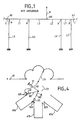
- FIG. 1 is a schematic view showing a diplexer according to the prior art which receives signals at two distinct frequencies F and F ′ respectively on a first and a second access, A1, A2, and delivers them to an antenna A connected to a third access A0.
- F is greater than F ′ so that, in what follows and in claims F and F ′ will be respectively called high frequency and low frequency and the frequencies around F and F ′ will be respectively called high frequencies and low frequencies.
- the access A1 receiving the signal at the frequency F is connected to the access A0 to which the antenna A is connected by a line which two separate connection points M and N separate into three sections of line: a section L connects the point M at access A1, a section L1 connects points M and N and a section L2 connects point N to access AO.
- two sections of line L3, L4, arranged in derivation connect the points M and N respectively to the ground.
- access A2 receiving the signal at frequency F ′ is connected to access AO by a line which two separate connection points M 'and N' separate into three line sections: a section L 'connects point M 'at the access A2, a section L1 ′ connects the points M' and N 'and a section L2 ′ connects the point N ′ to the antenna access, A0; moreover two sections of line L3 ′, L4 ′ connect points M 'and N' respectively to ground.
- the diplexer according to FIG. 1 comprises a diplexer proper constituted by the line sections L2, L4, L2 ′, L4 ′.
- the lengths of these sections are respectively ⁇ ′ / 4, ⁇ ′ / 2, ⁇ / 4, ⁇ / 2, where ⁇ and ⁇ ′ are the wavelengths corresponding to F and F ′; these values are theoretical values but the real values are very close.
- the diplexer according to FIG. 1 also includes two impedance matching circuits constituted respectively by the sections 1L, L3 and L1 ′, L3 ′.
- the introduction, in N ', of the line section L4 ′ leads to a mismatch; to readjust the antenna A with its line L4 ′, to the nominal impedance, it is necessary to place in M ′ the short-circuited line L3 ′.
- the length of the section L3 ′ is very close to that of the section L4′ and therefore of ⁇ / 2; the length of the section L1 ′ depends on the antenna impedance, seen in N ′ and on the line impedance of L2 ′.
- the line section L3 has a length of the order of ⁇ ′ / 2 and the length of L1 depends on the antenna impedance seen from N and the line impedance of L2.
- diplexers corresponding substantially, from the point of view of the lengths of line sections, to the diplexer according to FIG. 1, but in which the line sections L3, L4, L3 ′, L4 ′ are no longer short -circuited by earthing at one of their ends but are open at this end; it is also known to use diplexers in which one of the two channels, for example the low frequency channel, has short-circuited lines while the other channel has open lines.
- a circuit like that of FIG. 1, can only operate with two predetermined values respectively for F and F ′.
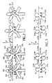
- FIG. 2 shows how the diplexer according to FIG. 1 can be modified to allow it to operate on four distinct values for its low frequency F ′ and four distinct values for its high frequency F.
- the low frequency channel of the diplexer according to FIG. 2 has been provided for ability to couple a transmitter working in the 11, 13, 15 and 17 MHz bands to the antenna while the high frequency channel has been designed to couple a transmitter working in the bands of 13, 15, 17 and 21 to the antenna MHz, which allows the antenna to work in the following pairs of bands: 11-13, 11-15, 11-17, 13-15, 13-17, 13-21, 15-17, 15-21 and 17-21; it should be noted that the pair 11-21 is not used because, the frequency ratio between the two bands being very close to 2, it is difficult to prevent harmonics 2 of the 11 MHz band from disturbing the 21 MHz band.
- the diplexer of FIG. 2 has the same line sections L, L ′, L1, L1 ′, L2, L2 ′, L3, L3 ′, L4, L4 ′, as that of FIG. 1, in a similar arrangement, but the length of the line sections can be modified so that the diplexer can be adjusted according to the frequencies F and F ′ indicated above.
- the low frequency channel that is to say in the channel which conducts the frequency signal F ′ to the antenna A
- the high frequency channel each comprise two switches: C1, C2 for the high channel frequencies, C1 ′, C2′ for the low frequency channel.
- Each switch is a rotary switch with two wafers with four pads per wafer, such as the pads P11 to P14 and P15 to P18 for the first and second wafer of the switch C1; a slider is associated with each wafer, such as the sliders J11 and J12 for the switch C1, which correspond to the wafers carrying the pads P11 to P14 and P15 to P18 respectively.
- the first of the two wafers of each switch has its pads in the connection between the two accesses A1, A2, and the successive pads of each first wafer are interconnected by sections of line; thus the pads P11 to P14 of the switch C1 are in series in this connection, thanks to line sections K11, K12 and K13 which respectively connect the pads P11 and P12, P12 and P13, P13 and P14.
- the second of the two wafers of each switch has its successive pads connected by sections of lines; thus the pads P15 to P18 of the switch C1 are connected by sections K16, K15, K14 disposed respectively between the pads P15 and P16, P16 and P17, P17 and P18.
- the cursor of the first wafer such as the cursor J11 of the switch C1 is connected to one of the two extreme pads of the second wafer while the other end pad and the slider of this wafer are connected to ground.
- the line sections relating to the switch C2, as well as the sliders and the pads of this switch, have been designated in FIG. 2 by adding 10 to the figure of the corresponding element relating to the switch C1, this is how the section K22 of switch C2 corresponds to section K12 of switch C1.
- the line sections of the first wafers that is to say the sections such as K21, which are in series between the accesses A1, A2, have been drawn in the form of rounds while the sections of the second wafers of the switches have been drawn in the form of slots.
- the four cursors of the high frequency channel determine a structure according to FIG. 1, in which the points M and N are the movable ends of the cursors of the first wafers of the switches C1 and C2 and in which the line sections L1, L2, L3, L4 of FIG. 1 are respectively constituted by the sections going from the block P13 to the block P23, from the block P23 to the access AO, from the block P13 to the ground including the section K14, and from stud P23 to ground including the section K24.
- the position occupied by the sliders of switches C1 and C2 is that which is provided when the signal F ′, on port A2, is in the 15 MHz band.
- the diplexer By moving the four sliders of the switches C1 and C2 simultaneously by one pad on the right (in the sense of a displacement in FIG. 2), or by one pad on the left, or by two pads on the left, the diplexer is set for a signal on access A2 whose frequency F ′ is respectively in the band of 17, 13 and 11 MHz.
- switches C1 ′, C2 ′ of the low frequency channel which are identical to those of the high frequency channel and the pads of the wafers of which are wired with line sections of which only the length is different by compared to the high frequency channel.
- the position of the cursors of the low frequency channel corresponds to a working signal, on the access A1, located in the 17 MHz band, while a displacement of all the cursors of the switches C1 ′ and C2′by one pad to the left, or one pad to the right, or two pads to the right would correspond to a working signal, on access A1, located respectively in the bands of 21, 15 and 13 MHz.
- the lengths of the sections are determined by considering a diplexer according to FIG. 1 in which the position of the points M, N, M ′, N 'would be adjustable according to the operating bands and in which the length of the short-circuited sections L3, L4, L3 ′, L4 ′ would also be adjustable.
- the length of the sections such as K11 and K25 can then be determined by simple subtractions taking into account the line lengths which constitute, for example, the cursor J1 of the switch C1 in series with the link going from this cursor to the pad P18 of the second wafer from the same switch.
- the lengths of the line sections between the two switches of the same channel are average lengths determined as a function of the antenna impedance at the average frequency of the frequencies of use.
- FIG. 2 For the sake of simplification, the conductive lines of the various attached figures have been represented by a single line, of course these are symmetrical lines, of the kind of two-wire lines, or asymmetrical, of the kind of coaxial lines.
- FIG. 2 was produced in two-wire lines, which amounts to saying that, to be complete, FIG. 2 should include lines represented by two parallel lines, double cursors with two parallel arms and double pancakes with two superimposed sets of four studs each.
- FIG. 3 is the diagram of an embodiment of a diplexer according to the invention associated with a multi-channel, broadband antenna, A, working in the bands of 13, 15, 17 and 21 MHz.
- this figure which corresponds to Figure 2 but with pancakes with three studs, only the marks relating to the antenna, A, and the access points, AO, A1, A2 have been marked so as not to overload the drawing and allow d '' indicate the lengths in meters of the different line sections.
- the high frequency channel that is to say the one corresponding to access A1
- the low frequency channel has been designed to work in the bands of 13, 15 and 17 MHz.
- the length of the sections in series between the line of access A1 and that of access A2 are respectively 1 -1.6 - 2.16 - 0.5 - 0.8 - 3.46 - 4.21 - 0.56 - 0.7 - 1 - 1.47 meters.
- the four branch line elements they each comprise three sections of line in series; the length of these sections, from the cursors relating to the first wafers (that is to say to the wafers relating to the sections in series between the accesses A1 and A2) is 6.92 - 1.5 and 1 meter in the high frequency channel and 8.42 - 1.13 and 1.45 meters in the low frequency channel.
- FIG. 4 shows a study of a switch of the type of the switch C1 of FIG. 2, when the line L3 has its end in open circuit and not to ground as in FIGS. 1 to 3. In this case the structure of the first wafer, with its cursor J11, remains unchanged.
- the second wafer with its cursor J21 is modified so that the line sections K14, K15, K16 have no electrical contact with the rest of the diplexer when they are not used; for this purpose the second wafer has studs, Q11, Q12, Q13, with two separate terminals and a cursor B with three branches B1, B2, B3 each cut by an isolator S1, S2, S3; the cursor B makes it possible to join the two terminals of the pad Q11 or of the pads Q11, Q12 or of the pads Q11, Q12, Q13 or of no pad; this cursor moves like the cursor J12 in FIG. 2 between four positions and its positions are linked to those that takes cursor J11 from the first cake.
- the cursors J11 and B can be moved together either from one position to the right, or from one or two positions to the left, so as to modify the setting of the diplexer as a function of the low operating frequency chosen.
- the present invention is not limited to the examples described, thus in particular that it applies to the case of diplexers intended to operate on a number of bands other than three or four, both at high frequencies and at low frequencies and, possibly for a different number of bands in high frequencies than that in low frequencies; it suffices that the two switches of a channel have the number of positions corresponding to the number of possible bands of the other channel.
Abstract
Description
La présente invention se rapporte à un diplexeur pour antenne à large bande et, en particulier, pour antenne fonctionnant en ondes décamétriques c'est-à-dire à des fréquences allant de 3 à 30 MHz.The present invention relates to a diplexer for broadband antenna and, in particular, for antenna operating in HF that is to say at frequencies ranging from 3 to 30 MHz.
En radiodiffusion, pour transmettre un même programme sur deux fréquences de canaux voisins et avec les mêmes caractéristiques de rayonnement, afin d'être sûr d'atteindre une zone géographique donnée, il est connu d'utiliser un diplexeur qui réalise la mise en parallèle de deux émetteurs sur une même antenne tout en évitant, ou du moins en rendant très faible, le couplage entre les deux émetteurs.In broadcasting, to transmit the same program on two frequencies of neighboring channels and with the same radiation characteristics, in order to be sure of reaching a given geographical area, it is known to use a diplexer which performs the paralleling of two transmitters on the same antenna while avoiding, or at least making very weak, the coupling between the two transmitters.
Les diplexeurs actuellement utilisés sont conçus pour effectuer le diplexage sur deux canaux donnés à une fréquence donnée dans chaque canal. Les antennes à large bande, "multicanaux", développées depuis plus de dix ans perdent donc beaucoup de leur intérêt si elles sont utilisées avec de tels diplexeurs.The diplexers currently used are designed to perform the diplexing on two given channels at a given frequency in each channel. Broadband, "multi-channel" antennas, developed for more than ten years therefore lose much of their interest if they are used with such diplexers.
Le but de la présente invention est d'éviter cet inconvénient en donnant la possibilité d'utiliser un même diplexeur pour différentes fréquences d'émission des deux émetteurs ce qui va donc nécessiter d'utiliser une antenne à large bande "multicanaux".The object of the present invention is to avoid this drawback by giving the possibility of using the same diplexer for different transmission frequencies of the two transmitters, which will therefore require the use of a "multi-channel" broadband antenna.
La présente invention a pour objet un diplexeur dont la longueur des éléments de ligne, qui le composent, est réglable, tel que défini par la revendication 1.The subject of the present invention is a diplexer, the length of the line elements of which it is composed is adjustable, as defined by claim 1.
D'autres objets et d'autres caractéristiques apparaîtront à l'aide de la description ci-après et des figures s'y rapportant qui représentent:
- - la figure 1 un schéma d'un diplexeur selon l'art antérieur,
- - les figures 2 et 3, des schémas de diplexeurs selon l'invention,
- - la figure 4, une partie d'un autre diplexeur selon l'invention
- FIG. 1 a diagram of a diplexer according to the prior art,
- FIGS. 2 and 3, diagrams of diplexers according to the invention,
- - Figure 4, part of another diplexer according to the invention
Sur les différentes figures les éléments correspondants sont désignés par les mêmes repères. De plus il est à noter que, pour des problèmes de place et de lisibilité, les proportions n'ont pas toujours été respectées dans les figures.In the various figures, the corresponding elements are designated by the same references. In addition, it should be noted that, for problems of space and readability, the proportions have not always been respected in the figures.
La figure 1 est une vue schématique montrant un diplexeur selon l'art connu qui reçoit des signaux à deux fréquences distinctes F et F′ respectivement sur un premier et un deuxième accès, A1, A2, et les délivre à une antenne A branchée sur un troisième accès A0. Dans l'exemple décrit F est supérieur à F′ si bien que, dans ce qui suit et dans les revendications F et F′ seront respectivement appelées fréquence haute et fréquence basse et les fréquences autour de F et de F′ seront respectivement appelées fréquences hautes et fréquences basses.FIG. 1 is a schematic view showing a diplexer according to the prior art which receives signals at two distinct frequencies F and F ′ respectively on a first and a second access, A1, A2, and delivers them to an antenna A connected to a third access A0. In the example described F is greater than F ′ so that, in what follows and in claims F and F ′ will be respectively called high frequency and low frequency and the frequencies around F and F ′ will be respectively called high frequencies and low frequencies.
L'accès A1 recevant le signal à la fréquence F est relié à l'accès A0 sur lequel est branché l'antenne A par une ligne que deux points de raccordement distincts M et N séparent en trois tronçons de ligne: un tronçon L relie le point M à l'accès A1, un tronçon L1 relie les points M et N et un tronçon L2 relie le point N à l'accès AO. De plus, deux tronçons de ligne L3, L4, disposés en dérivation, relient respectivement les points M et N à la masse.The access A1 receiving the signal at the frequency F is connected to the access A0 to which the antenna A is connected by a line which two separate connection points M and N separate into three sections of line: a section L connects the point M at access A1, a section L1 connects points M and N and a section L2 connects point N to access AO. In addition, two sections of line L3, L4, arranged in derivation, connect the points M and N respectively to the ground.
De même l'accès A2 recevant le signal à la fréquence F′ est relié à l'accès AO par une ligne que deux points de raccordement distincts M' et N' séparent en trois tronçons de ligne: un tronçon L' relie le point M' à l'accès A2, un tronçon L1′ relie les points M' et N' et un tronçon L2′ relie le point N′ à l'accès d'antenne, A0; de plus deux tronçons de ligne L3′, L4′ relient respectivement les points M' et N' à la masse.Similarly, access A2 receiving the signal at frequency F ′ is connected to access AO by a line which two separate connection points M 'and N' separate into three line sections: a section L 'connects point M 'at the access A2, a section L1 ′ connects the points M' and N 'and a section L2 ′ connects the point N ′ to the antenna access, A0; moreover two sections of line L3 ′, L4 ′ connect points M 'and N' respectively to ground.
Le diplexeur selon la figure 1 comporte un diplexeur proprement dit constitué par les tronçons de ligne L2, L4, L2′, L4′. Les longueurs de ces tronçons sont respectivement de λ′/4, λ′/2, λ/4, λ/2, où λ et λ′ sont les longueurs d'ondes correspondant à F et F′; ces valeurs sont des valeurs théoriques mais les valeurs réelles en sont très voisines.The diplexer according to FIG. 1 comprises a diplexer proper constituted by the line sections L2, L4, L2 ′, L4 ′. The lengths of these sections are respectively λ ′ / 4, λ ′ / 2, λ / 4, λ / 2, where λ and λ ′ are the wavelengths corresponding to F and F ′; these values are theoretical values but the real values are very close.
Le diplexeur selon la figure 1 comporte également deux circuits d'adaptation d'impédance constitués respectivement par les tronçons 1L, L3 et L1′, L3′. En effet, par exemple sur la voie des fréquences basses, l'introduction, en N', du tronçon de ligne L4′ amène une désadaptation; pour réadapter l'antenne A avec sa ligne L4′, à l'impédance nominale, il est nécessaire de placer en M′ la ligne court-circuitée L3′. La longueur du tronçon L3′ est très proche de celle du tronçon L4′et donc de λ/2; la longueur du tronçon L1′ dépend de l'impédance d'antenne, vue en N′ et de l'impédance de ligne de L2′. De même, dans le circuit d'adaptation constitué par les tronçons L1 et L3, le tronçon de ligne L3 a une longueur de l'ordre de λ′/2 et la longueur de L1 dépend de l'impédance d'antenne vue de N et de l'impédance de ligne de L2.The diplexer according to FIG. 1 also includes two impedance matching circuits constituted respectively by the sections 1L, L3 and L1 ′, L3 ′. Indeed, for example on the low frequency channel, the introduction, in N ', of the line section L4 ′ leads to a mismatch; to readjust the antenna A with its line L4 ′, to the nominal impedance, it is necessary to place in M ′ the short-circuited line L3 ′. The length of the section L3 ′ is very close to that of the section L4′ and therefore of λ / 2; the length of the section L1 ′ depends on the antenna impedance, seen in N ′ and on the line impedance of L2 ′. Similarly, in the adaptation circuit constituted by the sections L1 and L3, the line section L3 has a length of the order of λ ′ / 2 and the length of L1 depends on the antenna impedance seen from N and the line impedance of L2.
Il est également connu d'utiliser des diplexeurs correspondant sensiblement, du point de vue des longueurs des tronçons de ligne, au diplexeur selon la figure 1, mais dans lesquels les tronçons de ligne L3, L4, L3′, L4′ ne sont plus court-circuités par mise à la masse à une de leurs extrémités mais sont ouverts à cette extrémité; il est également connu d'utiliser des diplexeurs dans lesquels l'une des deux voies, par exemple la voie basses fréquences, présente des lignes court-circuitées tandis que l'autre voie présente des lignes ouvertes. Mais il est à noter que, généralement, pour les lignes où circulent de fortes puissances, c'est-à-dire dans le cas d'utilisation d'émetteurs de 100 kW et plus, les diplexeurs à lignes ouvertes ne sont généralement pas employés afin d'éviter des problèmes de rayonnement et d'effet Corona; ils peuvent cependant être utilisés, malgré ces inconvénients, lorsque le rapport des fréquences extrêmes d'utilisation est de l'ordre de 2 ou supérieur à 2.It is also known to use diplexers corresponding substantially, from the point of view of the lengths of line sections, to the diplexer according to FIG. 1, but in which the line sections L3, L4, L3 ′, L4 ′ are no longer short -circuited by earthing at one of their ends but are open at this end; it is also known to use diplexers in which one of the two channels, for example the low frequency channel, has short-circuited lines while the other channel has open lines. But it should be noted that, generally, for lines where high powers circulate, that is to say in the case of using transmitters of 100 kW and more, open line diplexers are generally not used to avoid radiation and Corona effects; they can however be used, despite these drawbacks, when the ratio of the extreme frequencies of use is of the order of 2 or greater than 2.
Un circuit, comme celui de la figure 1, ne peut fonctionner qu'avec deux valeurs prédéterminées respectivement pour F et F′.A circuit, like that of FIG. 1, can only operate with two predetermined values respectively for F and F ′.
La figure 2 montre comment le diplexeur selon la figure 1 peut être modifié pour lui permettre de fonctionner sur quatre valeurs distinctes pour sa fréquence basse F′ et quatre valeurs distinctes pour sa fréquence haute F. La figure 2 correspond à une étude d'un diplexeur destiné à être associé à une antenne multicanaux, à large bande, conçue pour les cinq bandes des 11, 13, 15, 17, 21 MHz; les largeurs de bande sont définies comme suit d'après les normes internationales:
bande 11 MHz = de 11,65 à 12,05 MHz = 3,43% de 11,65
bande 13 MHz = de 13,6 à 13,8 MHz = 1,47% de 13,6
bande 15 MHz = de 15,1 à 15,6 MHz = 3,31% de 15,1
bande 17 MHz = de 17,55 à 17,9 MHz = 1,99% de 17,55
bande 21 MHz = de 21,45 à 21,85 Mhz = 1,86% de 21,45.FIG. 2 shows how the diplexer according to FIG. 1 can be modified to allow it to operate on four distinct values for its low frequency F ′ and four distinct values for its high frequency F. FIG. 2 corresponds to a study of a diplexer intended to be associated with a multi-channel, broadband antenna, designed for the five bands of 11, 13, 15, 17, 21 MHz; the bandwidths are defined as follows according to international standards:
11 MHz band = from 11.65 to 12.05 MHz = 3.43% from 11.65
13 MHz band = from 13.6 to 13.8 MHz = 1.47% of 13.6
band 15 MHz = from 15.1 to 15.6 MHz = 3.31% of 15.1
band 17 MHz = from 17.55 to 17.9 MHz = 1.99% of 17.55
21 MHz band = from 21.45 to 21.85 MHz = 1.86% of 21.45.
Pour pouvoir utiliser toutes les possibilités de cette antenne, la voie basses fréquences du diplexeur selon la figure 2 a été prévue pour pouvoir coupler à l'antenne un émetteur travaillant dans les bandes des 11, 13, 15 et 17 MHz tandis que la voie hautes fréquences a été prévue pour coupler à l'antenne un émetteur travaillant dans les bandes des 13, 15, 17 et 21 MHz, ce qui permet de faire travailler l'antenne dans les couples de bandes suivants: 11-13, 11-15, 11-17, 13-15, 13-17, 13-21, 15-17, 15-21 et 17-21; il est à remarquer que le couple 11-21 n'est pas utilisé car, le rapport des fréquences entre les deux bandes étant très proche de 2, il est difficile d'empêcher que des harmoniques 2 de la bande des 11 MHz ne viennent perturber la bande des 21 MHz.To be able to use all the possibilities of this antenna, the low frequency channel of the diplexer according to FIG. 2 has been provided for ability to couple a transmitter working in the 11, 13, 15 and 17 MHz bands to the antenna while the high frequency channel has been designed to couple a transmitter working in the bands of 13, 15, 17 and 21 to the antenna MHz, which allows the antenna to work in the following pairs of bands: 11-13, 11-15, 11-17, 13-15, 13-17, 13-21, 15-17, 15-21 and 17-21; it should be noted that the pair 11-21 is not used because, the frequency ratio between the two bands being very close to 2, it is difficult to prevent
Pour permettre ces différents fonctionnements le diplexeur de la figure 2 comporte les mêmes tronçons de ligne L, L′, L1, L1′, L2, L2′, L3, L3′, L4, L4′, que celui de la figure 1, dans une disposition semblable, mais la longueur des tronçons de ligne peut être modifiée afin que le diplexeur puisse être réglé en fonction des fréquences F et F′ indiquées ci-avant. A cette fin, la voie basses fréquences, c'est-à-dire dans la voie qui conduit le signal de fréquence F′ à l'antenne A, et la voie hautes fréquences comportent chacune deux commutateurs: C1, C2 pour la voie hautes fréquences, C1′, C2′pour la voie basses fréquences. Chaque commutateur est un commutateur rotatif à deux galettes avec quatre plots par galette, tels que les plots P11 à P14 et P15 à P18 pour les première et seconde galette du commutateur C1; à chaque galette est associé un curseur, tels les curseurs J11 et J12 pour le commutateur C1, qui correspondent aux galettes portant respectivement les plots P11 à P14 et P15 à P18. La première des deux galettes de chaque commutateur a ses plots dans la liaison entre les deux accès A1, A2, et les plots successifs de chaque première galette sont reliés entre eux par des tronçons de ligne; ainsi les plots P11 à P14 du commutateur C1 se trouvent en série dans cette liaison, grâce à des tronçons de ligne K11, K12 et K13 qui relient respectivement les plots P11 et P12, P12 et P13, P13 et P14. La seconde des deux galettes de chaque commutateur a ses plots successifs reliés par des tronçons de lignes; ainsi les plots P15 à P18 du commutateur C1 sont reliés par des tronçons K16, K15, K14 disposés respectivement entre les plots P15 et P16, P16 et P17, P17 et P18.To allow these different operations, the diplexer of FIG. 2 has the same line sections L, L ′, L1, L1 ′, L2, L2 ′, L3, L3 ′, L4, L4 ′, as that of FIG. 1, in a similar arrangement, but the length of the line sections can be modified so that the diplexer can be adjusted according to the frequencies F and F ′ indicated above. To this end, the low frequency channel, that is to say in the channel which conducts the frequency signal F ′ to the antenna A, and the high frequency channel each comprise two switches: C1, C2 for the high channel frequencies, C1 ′, C2′ for the low frequency channel. Each switch is a rotary switch with two wafers with four pads per wafer, such as the pads P11 to P14 and P15 to P18 for the first and second wafer of the switch C1; a slider is associated with each wafer, such as the sliders J11 and J12 for the switch C1, which correspond to the wafers carrying the pads P11 to P14 and P15 to P18 respectively. The first of the two wafers of each switch has its pads in the connection between the two accesses A1, A2, and the successive pads of each first wafer are interconnected by sections of line; thus the pads P11 to P14 of the switch C1 are in series in this connection, thanks to line sections K11, K12 and K13 which respectively connect the pads P11 and P12, P12 and P13, P13 and P14. The second of the two wafers of each switch has its successive pads connected by sections of lines; thus the pads P15 to P18 of the switch C1 are connected by sections K16, K15, K14 disposed respectively between the pads P15 and P16, P16 and P17, P17 and P18.
Le curseur de la première galette, tel le curseur J11 du commutateur C1, est relié à un des deux plots extrêmes de la seconde galette tandis que l'autre plot extrême et le curseur de cette galette sont reliés à la masse. Les tronçons de ligne relatifs au commutateur C2, de même que les curseurs et les plots de ce commutateur, ont été désignés sur la figure 2 en ajoutant 10 au chiffre de l'élément correspondant relatif au commutateur C1, c'est ainsi que le tronçon K22 du commutateur C2 correspond au tronçon K12 du commutateur C1. Par ailleurs, pour faciliter la compréhension de la figure 2, de même que celle de la figure 3, les tronçons de ligne des premières galettes, c'est-à-dire les tronçons tels que K21, qui se trouvent en série entre les accès A1, A2, ont été dessinés sous forme d'arrondis tandis que les tronçons des secondes galettes des commutateurs ont été dessinés sous forme de créneaux.The cursor of the first wafer, such as the cursor J11 of the switch C1, is connected to one of the two extreme pads of the second wafer while the other end pad and the slider of this wafer are connected to ground. The line sections relating to the switch C2, as well as the sliders and the pads of this switch, have been designated in FIG. 2 by adding 10 to the figure of the corresponding element relating to the switch C1, this is how the section K22 of switch C2 corresponds to section K12 of switch C1. Furthermore, to facilitate the understanding of FIG. 2, as well as that of FIG. 3, the line sections of the first wafers, that is to say the sections such as K21, which are in series between the accesses A1, A2, have been drawn in the form of rounds while the sections of the second wafers of the switches have been drawn in the form of slots.
Dans la position qu'ils occupent sur la figure 2, les quatre curseurs de la voie hautes fréquences déterminent une structure selon la figure 1, dans laquelle les points M et N sont les extrémités mobiles des curseurs des premières galettes des commutateurs C1 et C2 et dans laquelle les tronçons de ligne L1, L2, L3, L4 de la figure 1 sont respectivement constitués par les tronçons allant du plot P13 au plot P23, du plot P23 à l'accès AO, du plot P13 à la masse en incluant le tronçon K14, et du plot P23 à la masse en incluant le tronçon K24. La position qu'occupent les curseurs des commutateurs C1 et C2 est celle qui est prévue lorsque le signal F′, sur l'accès A2, est dans la bande des 15 MHz. En déplaçant les quatre curseurs des commutateurs C1 et C2 simultanément d'un plot sur la droite (au sens d'un déplacement sur la figure 2), ou d'un plot sur la gauche, ou de deux plots sur la gauche, le diplexeur se trouve réglé pour un signal sur l'accès A2 dont la fréquence F′ se trouve respectivement dans la bande des 17, 13 et 11 MHz.In the position they occupy in FIG. 2, the four cursors of the high frequency channel determine a structure according to FIG. 1, in which the points M and N are the movable ends of the cursors of the first wafers of the switches C1 and C2 and in which the line sections L1, L2, L3, L4 of FIG. 1 are respectively constituted by the sections going from the block P13 to the block P23, from the block P23 to the access AO, from the block P13 to the ground including the section K14, and from stud P23 to ground including the section K24. The position occupied by the sliders of switches C1 and C2 is that which is provided when the signal F ′, on port A2, is in the 15 MHz band. By moving the four sliders of the switches C1 and C2 simultaneously by one pad on the right (in the sense of a displacement in FIG. 2), or by one pad on the left, or by two pads on the left, the diplexer is set for a signal on access A2 whose frequency F ′ is respectively in the band of 17, 13 and 11 MHz.
Des commentaires semblables pourraient être faits relativement aux commutateurs C1′, C2′ de la voie basses fréquences, qui sont identiques à ceux de la voie hautes fréquences et dont les plots des galettes sont câblés avec des tronçons de ligne dont seule la longueur est différente par rapport à la voie hautes fréquences. Il est à noter que la position des curseurs de la voie basses fréquences correspond à un signal de travail, sur l'accès A1, situé dans la bande des 17 MHz, tandis qu'un déplacement de l'ensemble des curseurs des commutateurs C1′et C2′d'un plot vers la gauche, ou d'un plot vers la droite, ou de deux plots vers la droite correspondrait à un signal de travail, sur l'accès A1, situé respectivement dans les bandes des 21, 15 et 13 MHz.Similar comments could be made with respect to switches C1 ′, C2 ′ of the low frequency channel, which are identical to those of the high frequency channel and the pads of the wafers of which are wired with line sections of which only the length is different by compared to the high frequency channel. It should be noted that the position of the cursors of the low frequency channel corresponds to a working signal, on the access A1, located in the 17 MHz band, while a displacement of all the cursors of the switches C1 ′ and C2′by one pad to the left, or one pad to the right, or two pads to the right would correspond to a working signal, on access A1, located respectively in the bands of 21, 15 and 13 MHz.
Les longueurs des tronçons, tels que K11 et K25, sont déterminées en considérant un diplexeur selon la figure 1 dans lequel la position des points M, N, M′, N' serait réglable en fonction des bandes de fonctionnement et dans lequel la longueur des tronçons court-circuités L3, L4, L3′, L4′ serait aussi réglable. Ainsi sont définies quatre positions pour chacun de ces points et quatre longueurs pour chaque tronçon en court-circuit; la longueur des tronçons tels que K11 et K25 peut alors être déterminée par de simples soustractions en tenant compte des longueurs de ligne que constituent, par exemple, le curseur J1 du commutateur C1 en série avec la liaison allant de ce curseur au plot P18 de la seconde galette de ce même commutateur. Les longueurs des tronçons de ligne entre les deux commutateurs dune même voie sont des longueurs moyennes déterminées en fonction de l'impédance de l'antenne à la fréquence moyenne des fréquences d'utilisation.The lengths of the sections, such as K11 and K25, are determined by considering a diplexer according to FIG. 1 in which the position of the points M, N, M ′, N 'would be adjustable according to the operating bands and in which the length of the short-circuited sections L3, L4, L3 ′, L4 ′ would also be adjustable. Thus, four positions are defined for each of these points and four lengths for each short-circuited section; the length of the sections such as K11 and K25 can then be determined by simple subtractions taking into account the line lengths which constitute, for example, the cursor J1 of the switch C1 in series with the link going from this cursor to the pad P18 of the second wafer from the same switch. The lengths of the line sections between the two switches of the same channel are average lengths determined as a function of the antenna impedance at the average frequency of the frequencies of use.
Par souci de simplification les lignes conductrices des différentes figures ci-jointes ont été représentées par un seul trait, bien entendu ce sont des lignes symétriques, du genre lignes bifilaires, ou asymétriques, du genre des lignes coaxiales. C'est ainsi que l'exemple selon la figure 2 a été réalisé en lignes bifilaires, ce qui revient à dire que, pour être complète la figure 2 devrait comporter des lignes représentées par deux traits parallèles, des curseurs doubles à deux bras parallèles et des galettes doubles à deux ensembles superposés de quatre plots chacun.For the sake of simplification, the conductive lines of the various attached figures have been represented by a single line, of course these are symmetrical lines, of the kind of two-wire lines, or asymmetrical, of the kind of coaxial lines. Thus the example according to FIG. 2 was produced in two-wire lines, which amounts to saying that, to be complete, FIG. 2 should include lines represented by two parallel lines, double cursors with two parallel arms and double pancakes with two superimposed sets of four studs each.
La figure 3 est le schéma d'une réalisation d'un diplexeur selon l'invention associé à une antenne multicanaux, à large bande, A, travaillant dans les bandes des 13, 15, 17 et 21 MHz. Sur cette figure, qui correspond à la figure 2 mais avec des galettes à trois plots, seuls les repères relatifs à l'antenne, A, et aux accès, AO, A1, A2 ont été marqués pour ne pas surcharger le dessin et permettre d'indiquer, les longueurs en mètres des différents tronçons de ligne.FIG. 3 is the diagram of an embodiment of a diplexer according to the invention associated with a multi-channel, broadband antenna, A, working in the bands of 13, 15, 17 and 21 MHz. In this figure, which corresponds to Figure 2 but with pancakes with three studs, only the marks relating to the antenna, A, and the access points, AO, A1, A2 have been marked so as not to overload the drawing and allow d '' indicate the lengths in meters of the different line sections.
Dans cette réalisation la voie hautes fréquences, c'est-à-dire celle correspondant à l'accès A1, a été conçue pour travailler dans les bandes des 15, 17 et 21 MHz, tandis que la voie basses fréquences a été conçue pour travailler dans les bandes des 13, 15 et 17 MHz.In this embodiment the high frequency channel, that is to say the one corresponding to access A1, was designed to work in bands of 15, 17 and 21 MHz, while the low frequency channel has been designed to work in the bands of 13, 15 and 17 MHz.
La longueur des tronçons en série entre la ligne de l'accès A1 et celle de l'accès A2 sont respectivement de 1 -1,6 - 2,16 - 0,5 - 0,8 -3,46 - 4,21 - 0,56 - 0,7 - 1 - 1,47 mètres. Quant aux quatre éléments de ligne en dérivation ils comportent chacun trois tronçons de ligne en série; la longueur de ces tronçons, à partir des curseurs relatifs aux premières galettes (c'est-à-dire aux galettes relatives aux tronçons en série entre les accès A1 et A2) est de 6,92 - 1,5 et 1 mètre dans la voie hautes fréquences et de 8,42 - 1,13 et 1,45 mètres dans la voie basses fréquences.The length of the sections in series between the line of access A1 and that of access A2 are respectively 1 -1.6 - 2.16 - 0.5 - 0.8 - 3.46 - 4.21 - 0.56 - 0.7 - 1 - 1.47 meters. As for the four branch line elements, they each comprise three sections of line in series; the length of these sections, from the cursors relating to the first wafers (that is to say to the wafers relating to the sections in series between the accesses A1 and A2) is 6.92 - 1.5 and 1 meter in the high frequency channel and 8.42 - 1.13 and 1.45 meters in the low frequency channel.
Le diplexeur qui a servi d'exemple à la réalisation selon la figure 3 présente les caractéristiques suivantes:
- - utilisation d'une antenne multicanaux d'impédance d'entrée étale à 150 ohms et de ROS (rapport d'onde stationnaire, standing-wave ratio ou SWR dans la littérature anglo-saxonne) au maximum égal à 2,
- - lignes symétriques 300 ohms
- - découplage entre les voies hautes et basses fréquences au moins de 30 dB ce qui, avec des émetteurs de 500 kW, laisse au plus 500 W dans la voie découplée, valeur tout à fait acceptable, qui n'empêche pas la mise en service du second émetteur branché sur le diplexeur lorsque le premier est déjà en fonctionnement.
- - use of a multichannel antenna with input impedance spread at 150 ohms and ROS (standing wave ratio, standing-wave ratio or SWR in Anglo-Saxon literature) at most equal to 2,
- - balanced lines 300 ohms
- - decoupling between the high and low frequency channels of at least 30 dB which, with 500 kW transmitters, leaves at most 500 W in the decoupled channel, a completely acceptable value, which does not prevent the commissioning of the second transmitter connected to the diplexer when the first is already in operation.
La figure 4 montre une étude d'un commutateur du genre du commutateur C1 de la figure 2, lorsque la ligne L3 a son extrémité en circuit ouvert et non pas à la masse comme sur les figures 1 à 3. Dans ce cas la structure de la première galette, avec son curseur J11, reste inchangée. Par contre la seconde galette avec son curseur J21 est modifiée de manière que les tronçons de ligne K14, K15, K16 n'aient aucun contact électrique avec le reste du diplexeur quand ils ne sont pas utilisés; à cet effet la seconde galette comporte des plots, Q11, Q12, Q13, à deux bornes distinctes et un curseur B à trois branches B1, B2, B3 coupées chacune par un isolateur S1, S2, S3; le curseur B permet de réunir les deux bornes du plot Q11 ou des plots Q11, Q12 ou des plots Q11, Q12, Q13 ou d'aucun plot; ce curseur se déplace comme le curseur J12 de la figure 2 entre quatre positions et ses positions sont liées à celles que prend le curseur J11 de la première galette. Ainsi, depuis la position qu'ils occupent sur la figure 4, les curseurs J11 et B peuvent être déplacés ensemble soit d'une position vers la droite, soit d'une ou deux positions vers la gauche, de manière à modifier le réglage du diplexeur en fonction de la fréquence basse de fonctionnement choisie.FIG. 4 shows a study of a switch of the type of the switch C1 of FIG. 2, when the line L3 has its end in open circuit and not to ground as in FIGS. 1 to 3. In this case the structure of the first wafer, with its cursor J11, remains unchanged. On the other hand, the second wafer with its cursor J21 is modified so that the line sections K14, K15, K16 have no electrical contact with the rest of the diplexer when they are not used; for this purpose the second wafer has studs, Q11, Q12, Q13, with two separate terminals and a cursor B with three branches B1, B2, B3 each cut by an isolator S1, S2, S3; the cursor B makes it possible to join the two terminals of the pad Q11 or of the pads Q11, Q12 or of the pads Q11, Q12, Q13 or of no pad; this cursor moves like the cursor J12 in FIG. 2 between four positions and its positions are linked to those that takes cursor J11 from the first cake. Thus, from the position they occupy in FIG. 4, the cursors J11 and B can be moved together either from one position to the right, or from one or two positions to the left, so as to modify the setting of the diplexer as a function of the low operating frequency chosen.
La présente invention n'est pas limitée aux exemples décrits, c'est ainsi en particulier qu'elle s'applique au cas de diplexeurs prévus pour fonctionner sur un nombre de bandes différent de trois ou quatre, aussi bien en fréquences hautes qu'en fréquences basses et, éventuellement pour un nombre de bandes différent en fréquences hautes de celui en fréquences basses; il suffit que les deux commutateurs d'une voie aient le nombre de positions correspondant au nombre de bandes possibles de l'autre voie.The present invention is not limited to the examples described, thus in particular that it applies to the case of diplexers intended to operate on a number of bands other than three or four, both at high frequencies and at low frequencies and, possibly for a different number of bands in high frequencies than that in low frequencies; it suffices that the two switches of a channel have the number of positions corresponding to the number of possible bands of the other channel.
De même il est possible, par exemple avec des lignes bifilaires d'utiliser des commutateurs à curseurs glissants et même de commander les déplacement des curseurs par un moteur asservi aux bandes de fonctionnement choisies et à des résultats de mesure effectuées sur le diplexeur. Dans le cas de la figure 4, c'est-à-dire dans le cas de diplexeurs à lignes ouvertes, le curseur glissant perd de son intérêt en ce qui concerne la seconde galette qui est relative à une ligne en circuit ouvert, étant donné que le curseur doit obligatoirement s'arrêter au niveau des deux bornes d'un même plot.Similarly, it is possible, for example with two-wire lines, to use switches with sliding cursors and even to control the movement of the cursors by a motor controlled by the selected operating bands and by measurement results carried out on the diplexer. In the case of FIG. 4, that is to say in the case of diplexers with open lines, the sliding cursor loses its interest as regards the second wafer which is relative to a line in open circuit, given that the cursor must stop at the two terminals of the same pad.
Claims (4)
Applications Claiming Priority (2)
| Application Number | Priority Date | Filing Date | Title |
|---|---|---|---|
| FR8917428A FR2656741B1 (en) | 1989-12-29 | 1989-12-29 | BROADBAND DIPLEXER, ESPECIALLY FOR HF WAVES. |
| FR8917428 | 1989-12-29 |
Publications (2)
| Publication Number | Publication Date |
|---|---|
| EP0435752A1 true EP0435752A1 (en) | 1991-07-03 |
| EP0435752B1 EP0435752B1 (en) | 1993-11-24 |
Family
ID=9389134
Family Applications (1)
| Application Number | Title | Priority Date | Filing Date |
|---|---|---|---|
| EP19900403698 Expired - Lifetime EP0435752B1 (en) | 1989-12-29 | 1990-12-20 | A wide band diplexer, especially for decameter waves |
Country Status (4)
| Country | Link |
|---|---|
| EP (1) | EP0435752B1 (en) |
| DE (1) | DE69004791T2 (en) |
| ES (1) | ES2046750T3 (en) |
| FR (1) | FR2656741B1 (en) |
Citations (3)
| Publication number | Priority date | Publication date | Assignee | Title |
|---|---|---|---|---|
| US2147807A (en) * | 1936-11-07 | 1939-02-21 | Mackay Radio & Telegraph Co | Transmission line |
| FR980157A (en) * | 1948-02-20 | 1951-05-09 | Rca Corp | System of transmission lines to operate two or more transmitters simultaneously on the same antenna |
| US3778731A (en) * | 1972-06-05 | 1973-12-11 | Cincinnati Electronics Corp | Tuning method for t-network couplers |
-
1989
- 1989-12-29 FR FR8917428A patent/FR2656741B1/en not_active Expired - Lifetime
-
1990
- 1990-12-20 DE DE1990604791 patent/DE69004791T2/en not_active Expired - Fee Related
- 1990-12-20 ES ES90403698T patent/ES2046750T3/en not_active Expired - Lifetime
- 1990-12-20 EP EP19900403698 patent/EP0435752B1/en not_active Expired - Lifetime
Patent Citations (3)
| Publication number | Priority date | Publication date | Assignee | Title |
|---|---|---|---|---|
| US2147807A (en) * | 1936-11-07 | 1939-02-21 | Mackay Radio & Telegraph Co | Transmission line |
| FR980157A (en) * | 1948-02-20 | 1951-05-09 | Rca Corp | System of transmission lines to operate two or more transmitters simultaneously on the same antenna |
| US3778731A (en) * | 1972-06-05 | 1973-12-11 | Cincinnati Electronics Corp | Tuning method for t-network couplers |
Non-Patent Citations (1)
| Title |
|---|
| IEEE TRANSACTIONS ON BROADCASTING vol. 34, no. 2, juin 1988, pages 193-200, New York, US; H. FALLIS et al.: "Practical Techniques for feeding two or more High power shortwave transmitters to one antenna" * |
Also Published As
| Publication number | Publication date |
|---|---|
| FR2656741A1 (en) | 1991-07-05 |
| DE69004791D1 (en) | 1994-01-05 |
| EP0435752B1 (en) | 1993-11-24 |
| DE69004791T2 (en) | 1994-03-17 |
| FR2656741B1 (en) | 1992-03-20 |
| ES2046750T3 (en) | 1994-02-01 |
Similar Documents
| Publication | Publication Date | Title |
|---|---|---|
| EP1863116B1 (en) | Broadband directional coupler | |
| US5155724A (en) | Dual mode diplexer/multiplexer | |
| US8405470B2 (en) | Diplexer synthesis using composite right/left-handed phase-advance/delay lines | |
| US2270416A (en) | Electrical wave system | |
| EP0888647B1 (en) | Helix antenna with a built-in broadband power supply, and manufacturing methods therefor | |
| EP0243289A1 (en) | Plate antenna with two crossed polarizations | |
| FR2709603A1 (en) | Improvements to devices sensitive to electromagnetic radiation. | |
| FR2549283A1 (en) | IMPEDANCE TRANSFORMER, BROADBAND, TRANSFORMATION REPORT NEIGHBORING THREE, FOR RADIO FREQUENCIES | |
| FR2762729A1 (en) | RF POWER DIVIDER | |
| EP0888648B1 (en) | Helical antenna with built-in duplexing means, and manufacturing methods therefore | |
| EP1429458A2 (en) | Balun transformer with frequency selection | |
| EP2178152A1 (en) | Electronic switching device for high-frequency signals | |
| FR2799310A1 (en) | METHOD FOR CALIBRATING A COLLECTIVE ANTENNA | |
| EP0435752B1 (en) | A wide band diplexer, especially for decameter waves | |
| EP3176875A1 (en) | Active antenna architecture with reconfigurable hybrid beam formation | |
| EP0472483A1 (en) | Bidirectional duplexer for polarised microwaves, particularly realised in monolithic technology on gallium arsenide | |
| FR3004007A1 (en) | BROADBAND COUPLER | |
| EP0118357B1 (en) | Electronic antenna array for a cellular radio telephone network with fixed base stations, and with mobile and portable units | |
| US4264908A (en) | Adaptive polarization separation | |
| GB362472A (en) | Improvements in electrical transmission devices | |
| JP3051732B1 (en) | Microwave diplexer | |
| FR2607639A1 (en) | HIGH SELECTIVITY BAND REJECTOR AND USE OF SUCH A REJECTOR | |
| Sarma et al. | Receiver system of the ooty radio telescope | |
| EP2515373B1 (en) | Compact, lightweight frequency duplexer | |
| FR2556508A1 (en) | Balun connection from coax to symmetrical pair |
Legal Events
| Date | Code | Title | Description |
|---|---|---|---|
| PUAI | Public reference made under article 153(3) epc to a published international application that has entered the european phase |
Free format text: ORIGINAL CODE: 0009012 |
|
| AK | Designated contracting states |
Kind code of ref document: A1 Designated state(s): CH DE ES GB LI |
|
| 17P | Request for examination filed |
Effective date: 19911220 |
|
| 17Q | First examination report despatched |
Effective date: 19930322 |
|
| GRAA | (expected) grant |
Free format text: ORIGINAL CODE: 0009210 |
|
| AK | Designated contracting states |
Kind code of ref document: B1 Designated state(s): CH DE ES GB LI |
|
| PGFP | Annual fee paid to national office [announced via postgrant information from national office to epo] |
Ref country code: ES Payment date: 19931227 Year of fee payment: 4 |
|
| REF | Corresponds to: |
Ref document number: 69004791 Country of ref document: DE Date of ref document: 19940105 |
|
| GBT | Gb: translation of ep patent filed (gb section 77(6)(a)/1977) |
Effective date: 19931220 |
|
| REG | Reference to a national code |
Ref country code: ES Ref legal event code: FG2A Ref document number: 2046750 Country of ref document: ES Kind code of ref document: T3 |
|
| REG | Reference to a national code |
Ref country code: CH Ref legal event code: PUE Owner name: THOMSON-CSF |
|
| RAP2 | Party data changed (patent owner data changed or rights of a patent transferred) |
Owner name: THOMSON-CSF |
|
| PLBE | No opposition filed within time limit |
Free format text: ORIGINAL CODE: 0009261 |
|
| STAA | Information on the status of an ep patent application or granted ep patent |
Free format text: STATUS: NO OPPOSITION FILED WITHIN TIME LIMIT |
|
| 26N | No opposition filed | ||
| PGFP | Annual fee paid to national office [announced via postgrant information from national office to epo] |
Ref country code: CH Payment date: 19941118 Year of fee payment: 5 |
|
| PGFP | Annual fee paid to national office [announced via postgrant information from national office to epo] |
Ref country code: GB Payment date: 19941121 Year of fee payment: 5 Ref country code: DE Payment date: 19941121 Year of fee payment: 5 |
|
| PG25 | Lapsed in a contracting state [announced via postgrant information from national office to epo] |
Ref country code: ES Free format text: LAPSE BECAUSE OF EXPIRATION OF PROTECTION Effective date: 19941221 |
|
| PG25 | Lapsed in a contracting state [announced via postgrant information from national office to epo] |
Ref country code: GB Effective date: 19951220 |
|
| PG25 | Lapsed in a contracting state [announced via postgrant information from national office to epo] |
Ref country code: LI Effective date: 19951231 Ref country code: CH Effective date: 19951231 |
|
| GBPC | Gb: european patent ceased through non-payment of renewal fee |
Effective date: 19951220 |
|
| REG | Reference to a national code |
Ref country code: CH Ref legal event code: PL |
|
| PG25 | Lapsed in a contracting state [announced via postgrant information from national office to epo] |
Ref country code: DE Effective date: 19960903 |
|
| REG | Reference to a national code |
Ref country code: ES Ref legal event code: FD2A Effective date: 20010301 |