EP0429140B1 - Digitale Synchronisieranordnung - Google Patents
Digitale Synchronisieranordnung Download PDFInfo
- Publication number
- EP0429140B1 EP0429140B1 EP90203055A EP90203055A EP0429140B1 EP 0429140 B1 EP0429140 B1 EP 0429140B1 EP 90203055 A EP90203055 A EP 90203055A EP 90203055 A EP90203055 A EP 90203055A EP 0429140 B1 EP0429140 B1 EP 0429140B1
- Authority
- EP
- European Patent Office
- Prior art keywords
- pulse
- phase
- locked loop
- signal
- switching signal
- Prior art date
- Legal status (The legal status is an assumption and is not a legal conclusion. Google has not performed a legal analysis and makes no representation as to the accuracy of the status listed.)
- Expired - Lifetime
Links
- 230000001360 synchronised effect Effects 0.000 claims description 26
- 238000005070 sampling Methods 0.000 claims description 6
- 230000001419 dependent effect Effects 0.000 claims description 2
- 239000000203 mixture Substances 0.000 description 10
- 238000010586 diagram Methods 0.000 description 5
- 230000000903 blocking effect Effects 0.000 description 4
- 238000000034 method Methods 0.000 description 4
- 230000002123 temporal effect Effects 0.000 description 2
- 238000001514 detection method Methods 0.000 description 1
- 230000010355 oscillation Effects 0.000 description 1
- 230000010363 phase shift Effects 0.000 description 1
- 238000000926 separation method Methods 0.000 description 1
- 230000001629 suppression Effects 0.000 description 1
- 238000011144 upstream manufacturing Methods 0.000 description 1
Images

Classifications
-
- H—ELECTRICITY
- H04—ELECTRIC COMMUNICATION TECHNIQUE
- H04N—PICTORIAL COMMUNICATION, e.g. TELEVISION
- H04N5/00—Details of television systems
- H04N5/04—Synchronising
- H04N5/06—Generation of synchronising signals
-
- H—ELECTRICITY
- H04—ELECTRIC COMMUNICATION TECHNIQUE
- H04N—PICTORIAL COMMUNICATION, e.g. TELEVISION
- H04N5/00—Details of television systems
- H04N5/04—Synchronising
- H04N5/12—Devices in which the synchronising signals are only operative if a phase difference occurs between synchronising and synchronised scanning devices, e.g. flywheel synchronising
- H04N5/126—Devices in which the synchronising signals are only operative if a phase difference occurs between synchronising and synchronised scanning devices, e.g. flywheel synchronising whereby the synchronisation signal indirectly commands a frequency generator
Definitions
- the invention relates to a digital synchronizing arrangement for an image display device with a synchronizing signal isolating stage, in which horizontal synchronizing pulses are obtained from a digital television signal containing a synchronizing arrangement and supplied to the synchronizing arrangement, and to a phase locked loop, to which the horizontal synchronizing pulses are fed for the purpose of their synchronization.
- a digitally operating synchronization arrangement is known from EP-A-0 329 576, in which a window is opened at the times at which synchronization pulses are expected. It is then observed over a number of 32 image lines whether synchronous pulses occur in this window. If this is the case over 32 image lines, the phase-locked loop is assumed to coincide with the synchronous signal. In the opposite case, the synchronous impulses will not appear within this window over 32 picture lines, assuming that there is no coincidence. The synchronizing pulses supplied to the phase locked loop itself are not changed. It also does not solve the problems mentioned at the outset, in order to ensure reliable synchronization in the case of a disturbed or noisy television signal. Rather, if the synchronization is no longer correct, the phase-locked loop is switched to free oscillation.
- the latter supplies output signals which are in a defined phase position with respect to the horizontal synchronizing pulses and which can be used in a known manner, for example, for a deflection unit of an image display device.
- a second switching signal is generated, which delivers a pulse at a predetermined time interval after each pulse of the first switching signal.
- the generation of this second switching signal can be obtained, for example, by a time delay of the first switching signal or, like the first switching signal, from signals from the phase locked loop.
- This synchronizing arrangement has the main advantage over the known ones that within a window, which is formed here by the leading edges of the pulses of the first switching signal and the leading edges of the pulses of the second switching signal, only exactly one pulse is forwarded to the phase locked loop.
- Another advantage is that in the event of a strongly disturbed signal or phase jumps, which occur in particular when playing television signals from video recorders, the arrangement is nevertheless able to carry out a perfect synchronization, since then horizontal synchronizing pulses which are no longer during the Duration of the pulse of the first switching signal occur, but are still forwarded to the phase-locked loop, even if the window itself would already be closed, that is, if the pulse of the second switching signal has already occurred.
- the arrangement is therefore normal, i.e. So if the phase-locked loop is properly synchronized to the television signal and the horizontal synchronizing mixture contained in it and this is undisturbed, it is able to ensure perfect synchronization, since only exactly one horizontal synchronizing pulse is passed on to the phase-locked loop. If these conditions are not met, all horizontal synchronizing pulses that occur between two pulses of the first switching signal are forwarded to the phase-locked loop in order to enable its synchronization.
- the horizontal synchronizing pulses are fed to a first input of a first AND gate and a first input of a second AND gate, the second input of which is supplied with the first switching signal and the output of which is connected to the RESET input an RS flip-flop is connected, the SET input of which is supplied with the second switching signal and the output of which is connected to the second input of the first AND gate, the output signal of which is fed to the phase-locked loop.
- the second AND gate then delivers an output signal if a horizontal synchronizing pulse occurs during a pulse of the first switching signal.
- the RS flip-flop is then reset, whereupon the first AND gate blocks any horizontal synchronizing pulses that may still occur. This blocking is only released when a pulse of the second switching signal occurs, by which the RS flip-flop is set again, so that the blocking of the first AND gate is released.
- This circuit is easy to integrate with a simple structure.
- a register is connected upstream of the first input of the AND gate and the input of the phase-locked loop, both of which are clocked with the sampling clock of the television signal.
- both switching signals are generated by means of a counter provided in the phase comparator of the phase-locked loop, which is clocked with the sampling clocks of the television signal and is synchronized to the horizontal synchronous pulses in the synchronized state of the phase-locked loop.
- Phase control loops built entirely in digital technology cf. the parallel application EP-A-0 410 523 mostly have phase comparators in which a counter is provided. In such phase comparators, this counter serves to check during certain counter readings whether the phase-locked loop is correctly synchronized with the input signal. The input signal must then occur during certain counter readings. Since the counter reading of this counter is in the synchronized state of the phase-locked loop in a fixed relationship to the pulses occurring, the counter reading can be used simultaneously to generate the two switching signals at the desired times and in the desired duration. No additional effort is then required to generate the two switching signals.
- the predefinable time interval of each pulse of the second switching signal to the previous pulse of the first switching signal is 50 to 75 »sec. This time interval between the pulse of the second signal and the leading edge of the previous pulse of the first switching signal has proven to be advantageous for television signals, since in this way a very good suppression of interference pulses is achieved. On the other hand, the lock is not made so long that a safe synchronization is no longer possible.
- a digital synchronizing arrangement shown in FIG. 1 has a synchronizing signal separation stage on the input side, which is constructed by means of a low-pass filter 1 and a cutting level comparator 2.
- the low-pass filter 1 is supplied with a television signal which contains a horizontal synchronous mixture.
- the comparator 2 is connected downstream of the low-pass filter and has the task of comparing the signal supplied by the low-pass filter with a cutting level. In this way, the horizontal synchronizing pulses from the remaining television signal separated. These pulses separated in this way are then fed to a counter 3, which generates pulses of a defined width. These pulses of a defined width, which represent the horizontal synchronizing pulses, are fed to an edge detector 4.
- the output signal of the edge detector 4 is fed to a first input 5 of a first AND gate 6 and an input 7 of a register 8.
- the register 8 is clocked by means of a clock signal Clk.
- An output 9 of the register 8 is connected to a first input 10 of a second AND gate 11, the output 12 of which is connected to the RESET input 13 of an RS flip-flop 14.
- An output 15 of the RS flip-flop is connected to a second input 16 of the first AND gate 6.
- An output 17 of the first AND gate is connected to an input 18 of a register 19 which, like the register 8, is clocked by means of a clock signal Clk.
- An output 20 of the register 19 is fed to an input 21 of a phase locked loop 22, which is shown only schematically in the figure.
- the phase-locked loop 22 supplies a signal at its output 23, which can be fed, for example, to a horizontal deflection unit of an image display device, not shown in the figure.
- a first switching signal which appears at an output 24 of the phase locked loop 22
- a second switching signal which appears at a further output 25 of the phase locked loop
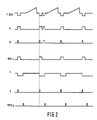
- a curve marked FBAS in FIG. 2 represents the input signal that is fed to the low-pass filter 1. It is the complete television signal, which contains four horizontal sync pulses and the active image information in between in the temporal section shown. In the example shown in FIG. 2, the horizontal synchronous mixture is disturbed in the second blanking interval.
- the output signal of the comparator 2 is shown in a curve A shown in FIG. 2, in which the CVBS signal is compared with a fixed cutting level and in which pulses are generated from the horizontal synchronous mixture.
- curve A shown in the figure it can already be seen that two pulses are generated in the second blanking interval.
- a curve B shown in FIG. 2 shows the output signal of the counter 3, in which pulses of a defined width are generated. These are the horizontal sync pulses. In the second blanking interval of the time segment shown in FIG. 2, two horizontal synchronizing pulses are generated due to the disturbed FBAS signal.
- the phase locked loop 22 shown in FIG. 1 delivers a first switching signal, which is designated in FIG. 2 with HPLL1.
- This first switching signal delivers a pulse precisely when horizontal synchronizing pulses are expected. If the phase-locked loop is correctly synchronized to the TV signal FBAS, then that is Phase locked loop is able to generate a pulse of the first switching signal precisely at the times when a horizontal synchronizing pulse is expected in the synchronous signal mixture. Since the width of the pulses contained in the horizontal synchronous mixture is known, the pulses of the first switching signal can be generated in the same width.
- a pulse of a second switching signal is generated, which is designated in FIG. 2 with HPLL2.
- a horizontal synchronous pulse according to curve B occurs simultaneously with a pulse of the first switching signal HPLL 1.
- These two signals which are supplied to the AND gate 11, cause the flip-flop 14 to be reset.
- the output signal of the flip-flop 14 is shown in the curve C. While this output signal of the flip-flop C is low, the AND gate 6 is blocked, so that no further horizontal synchronizing pulse can reach the phase locked loop 22.
- the horizontal synchronizing pulse which occurred during the duration of the pulse of the first switching signal HPLL 1, could still pass through the AND gate 6 and be read into the register 19, since the gate 11 and the flip-flop 14 have run times.
- the pulse is supplied to the second AND gate 11 only with the delay of a clock, which was carried out in the register 8.
- the flip-flop 14 is also reset only one clock later and the AND gate 6 is blocked only one clock after the horizontal synchronizing pulse has occurred.
- a pulse then appears at the output of register 19, which pulse is fed to the phase-locked loop and which is denoted by S in FIG. 2.
- the process described above as it occurs with an undisturbed input signal, as is the case, for example, in the period shown in FIG. 2 during the first blanking interval, means that when a horizontal synchronizing pulse occurs during a pulse of the first switching signal HPLL 1 to the occurrence of the second switching signal HPLL2, the AND gate 6 no further horizontal synchronous pulses to the register 19 or the phase locked loop 22.
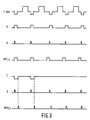
- the digital synchronizing arrangement shown in Fig. 1 has the additional advantage that it does not block despite the windowing in the event of phase jumps in the television signal, but the horizontal synchronizing pulses, even if they are outside the window, ie outside the period between the pulses of the first and the second switching signal are forwarded to the phase locked loop. This is explained below with reference to the pulse diagram shown in FIG. 3.
Landscapes
- Engineering & Computer Science (AREA)
- Multimedia (AREA)
- Signal Processing (AREA)
- Synchronizing For Television (AREA)
Applications Claiming Priority (2)
| Application Number | Priority Date | Filing Date | Title |
|---|---|---|---|
| DE3938887 | 1989-09-24 | ||
| DE3938887A DE3938887A1 (de) | 1989-11-24 | 1989-11-24 | Digitale synchronisieranordnung |
Publications (3)
| Publication Number | Publication Date |
|---|---|
| EP0429140A2 EP0429140A2 (de) | 1991-05-29 |
| EP0429140A3 EP0429140A3 (en) | 1991-09-04 |
| EP0429140B1 true EP0429140B1 (de) | 1995-02-22 |
Family
ID=6394092
Family Applications (1)
| Application Number | Title | Priority Date | Filing Date |
|---|---|---|---|
| EP90203055A Expired - Lifetime EP0429140B1 (de) | 1989-11-24 | 1990-11-19 | Digitale Synchronisieranordnung |
Country Status (6)
| Country | Link |
|---|---|
| US (1) | US5136384A (fa) |
| EP (1) | EP0429140B1 (fa) |
| JP (1) | JP3092938B2 (fa) |
| KR (1) | KR100190788B1 (fa) |
| DE (2) | DE3938887A1 (fa) |
| TW (1) | TW215506B (fa) |
Cited By (1)
| Publication number | Priority date | Publication date | Assignee | Title |
|---|---|---|---|---|
| EP0933938A3 (en) * | 1998-01-29 | 2005-01-05 | Victor Company Of Japan Limited | Apparatus and method of generating synchronizing pulse |
Families Citing this family (5)
| Publication number | Priority date | Publication date | Assignee | Title |
|---|---|---|---|---|
| WO1994010807A1 (en) * | 1992-11-05 | 1994-05-11 | Ampex Systems Corporation | Method and apparatus for providing noise immunity for an input interface of a digital video recorder |
| CA2109251A1 (en) * | 1993-10-26 | 1995-04-27 | Bryan Bruins | Self-adjusting window circuit with timing control |
| US5754251A (en) * | 1995-12-12 | 1998-05-19 | Trw Inc. | Digital video vertical synchronization pulse detector |
| JP4707207B2 (ja) * | 2000-04-14 | 2011-06-22 | 三菱電機株式会社 | オーバーレイ装置 |
| JP2006135749A (ja) * | 2004-11-08 | 2006-05-25 | Matsushita Electric Ind Co Ltd | 同期信号発生装置およびそれを備えた映像信号処理装置 |
Family Cites Families (8)
| Publication number | Priority date | Publication date | Assignee | Title |
|---|---|---|---|---|
| US4446482A (en) * | 1982-04-05 | 1984-05-01 | Zenith Radio Corporation | System for generating 2H pulses in a television receiver |
| FR2556903B1 (fr) * | 1983-12-15 | 1986-04-11 | Telediffusion Fse | Procede et circuits de regeneration d'instants significatifs d'un signal periodique |
| DE3443925C1 (de) * | 1984-12-01 | 1986-01-30 | Philips Patentverwaltung Gmbh, 2000 Hamburg | Schaltungsanordnung zum Unterscheiden der beiden Halbbilder in einem Fernsehsignal |
| US4639780A (en) * | 1985-04-01 | 1987-01-27 | Rca Corporation | Television synchronizing apparatus |
| US4872055A (en) * | 1987-02-04 | 1989-10-03 | U. S. Philips Corporation | Line synchronizing circuit in a picture display device |
| FR2627655B1 (fr) * | 1988-02-19 | 1990-07-27 | Sgs Thomson Microelectronics | Circuit de reconnaissance de synchronisation ligne |
| ES2056168T3 (es) * | 1988-09-02 | 1994-10-01 | Sanyo Electric Co | Circuito de sincronizacion de fase en un receptor de señal de video y metodo de obtencion de la sincronizacion de fase. |
| JP2584309B2 (ja) * | 1988-09-07 | 1997-02-26 | 三洋電機株式会社 | 基準信号作成回路 |
-
1989
- 1989-11-24 DE DE3938887A patent/DE3938887A1/de not_active Withdrawn
-
1990
- 1990-11-19 DE DE59008519T patent/DE59008519D1/de not_active Expired - Fee Related
- 1990-11-19 EP EP90203055A patent/EP0429140B1/de not_active Expired - Lifetime
- 1990-11-20 US US07/616,446 patent/US5136384A/en not_active Expired - Lifetime
- 1990-11-21 JP JP02314482A patent/JP3092938B2/ja not_active Expired - Fee Related
- 1990-11-22 KR KR1019900018929A patent/KR100190788B1/ko not_active Expired - Fee Related
- 1990-12-12 TW TW079110461A patent/TW215506B/zh active
Cited By (1)
| Publication number | Priority date | Publication date | Assignee | Title |
|---|---|---|---|---|
| EP0933938A3 (en) * | 1998-01-29 | 2005-01-05 | Victor Company Of Japan Limited | Apparatus and method of generating synchronizing pulse |
Also Published As
| Publication number | Publication date |
|---|---|
| DE59008519D1 (de) | 1995-03-30 |
| TW215506B (fa) | 1993-11-01 |
| JP3092938B2 (ja) | 2000-09-25 |
| EP0429140A2 (de) | 1991-05-29 |
| DE3938887A1 (de) | 1991-05-29 |
| KR910011006A (ko) | 1991-06-29 |
| US5136384A (en) | 1992-08-04 |
| JPH03175877A (ja) | 1991-07-30 |
| EP0429140A3 (en) | 1991-09-04 |
| KR100190788B1 (ko) | 1999-06-01 |
Similar Documents
| Publication | Publication Date | Title |
|---|---|---|
| DE2618031C2 (de) | Auswerteschaltung für Binärdaten | |
| DE69226943T2 (de) | Zusatzvideodatentrenner | |
| DE3690492C2 (de) | Phasenkomparator-Einrasterfassungsschaltung und unter Verwendung einer solchen Schaltung aufgebauter Frequenzsynthesegenerator | |
| DE2144551A1 (de) | Synchronisierschaltung | |
| DE2725998A1 (de) | Vertikalsynchronisierschaltung | |
| EP0464230B1 (de) | Digitale Phasenregelungsschleife | |
| DE2316260C3 (de) | Vorrichtung zum Erzeugen eines Synchronsignals für eine Fernsehanlage | |
| DE69121322T2 (de) | Schaltung zur Trennung eines horizontalen Synchronisierungssignals für ein Anzeigegerät | |
| DE68906050T2 (de) | Erkennungsschaltung zur Zeilensynchronisierung. | |
| EP0429140B1 (de) | Digitale Synchronisieranordnung | |
| DE2622635B2 (de) | Schaltungsanordnung zur Bildung | |
| DE2726037A1 (de) | Vertikalsynchronisierschaltung | |
| DE69106920T2 (de) | Vorrichtung zur Erzeugung von Zeitbasisfehlersignal. | |
| DE3327114C2 (de) | Pulsgenerator zur Erzeugung von Abtastimpulsen | |
| DE69613282T2 (de) | Vorrichtung zur ableitung eines taktsignals aus einem synchronsignal und videoaufzeichnungsgerät ausgestattet mit einer derartigen schaltungsanordnung | |
| EP0420320B1 (de) | Digitale Schaltungsanordnung zur Detektion von Synchronisationsimpulsen | |
| EP0420321B1 (de) | Synchronsignal-Detektor | |
| DE3631801C2 (de) | Automatische Phasenregelschaltung insbesondere für ein Videomagnetbandgerät | |
| DE19830130B4 (de) | Schaltungsanordnung für eine PLL-Schaltung (Phase-locked-Loop) zur Frequenzvervielfachung | |
| EP0410523B1 (de) | Synchronisieranordnung für ein Bildwiedergabegerät | |
| DE69223966T2 (de) | Gegen grosse Videosignalphasenverschiebungen unempfindlicher Horizontalzeilenzähler | |
| DE3921731C2 (fa) | ||
| DE69708531T2 (de) | Detektor für ein vertikales Synchronisationssignal | |
| DE2948785C2 (de) | Vertikalsynchronsignal-Detektorschaltung | |
| DE4316494C1 (de) | Digitale Taktsynchronisierung |
Legal Events
| Date | Code | Title | Description |
|---|---|---|---|
| PUAI | Public reference made under article 153(3) epc to a published international application that has entered the european phase |
Free format text: ORIGINAL CODE: 0009012 |
|
| AK | Designated contracting states |
Kind code of ref document: A2 Designated state(s): DE FR GB IT |
|
| PUAL | Search report despatched |
Free format text: ORIGINAL CODE: 0009013 |
|
| AK | Designated contracting states |
Kind code of ref document: A3 Designated state(s): DE FR GB IT |
|
| 17P | Request for examination filed |
Effective date: 19920228 |
|
| 17Q | First examination report despatched |
Effective date: 19931122 |
|
| GRAA | (expected) grant |
Free format text: ORIGINAL CODE: 0009210 |
|
| AK | Designated contracting states |
Kind code of ref document: B1 Designated state(s): DE FR GB IT |
|
| REF | Corresponds to: |
Ref document number: 59008519 Country of ref document: DE Date of ref document: 19950330 |
|
| ITF | It: translation for a ep patent filed | ||
| GBT | Gb: translation of ep patent filed (gb section 77(6)(a)/1977) |
Effective date: 19950511 |
|
| ET | Fr: translation filed | ||
| PLBE | No opposition filed within time limit |
Free format text: ORIGINAL CODE: 0009261 |
|
| STAA | Information on the status of an ep patent application or granted ep patent |
Free format text: STATUS: NO OPPOSITION FILED WITHIN TIME LIMIT |
|
| 26N | No opposition filed | ||
| REG | Reference to a national code |
Ref country code: FR Ref legal event code: CD |
|
| REG | Reference to a national code |
Ref country code: GB Ref legal event code: IF02 |
|
| REG | Reference to a national code |
Ref country code: GB Ref legal event code: 746 Effective date: 20020917 |
|
| REG | Reference to a national code |
Ref country code: FR Ref legal event code: D6 |
|
| PGFP | Annual fee paid to national office [announced via postgrant information from national office to epo] |
Ref country code: FR Payment date: 20021125 Year of fee payment: 13 |
|
| PGFP | Annual fee paid to national office [announced via postgrant information from national office to epo] |
Ref country code: GB Payment date: 20021129 Year of fee payment: 13 |
|
| PG25 | Lapsed in a contracting state [announced via postgrant information from national office to epo] |
Ref country code: GB Free format text: LAPSE BECAUSE OF NON-PAYMENT OF DUE FEES Effective date: 20031119 |
|
| PGFP | Annual fee paid to national office [announced via postgrant information from national office to epo] |
Ref country code: DE Payment date: 20040121 Year of fee payment: 14 |
|
| GBPC | Gb: european patent ceased through non-payment of renewal fee |
Effective date: 20031119 |
|
| PG25 | Lapsed in a contracting state [announced via postgrant information from national office to epo] |
Ref country code: FR Free format text: LAPSE BECAUSE OF NON-PAYMENT OF DUE FEES Effective date: 20040730 |
|
| REG | Reference to a national code |
Ref country code: FR Ref legal event code: ST |
|
| PG25 | Lapsed in a contracting state [announced via postgrant information from national office to epo] |
Ref country code: DE Free format text: LAPSE BECAUSE OF NON-PAYMENT OF DUE FEES Effective date: 20050601 |
|
| PG25 | Lapsed in a contracting state [announced via postgrant information from national office to epo] |
Ref country code: IT Free format text: LAPSE BECAUSE OF NON-PAYMENT OF DUE FEES;WARNING: LAPSES OF ITALIAN PATENTS WITH EFFECTIVE DATE BEFORE 2007 MAY HAVE OCCURRED AT ANY TIME BEFORE 2007. THE CORRECT EFFECTIVE DATE MAY BE DIFFERENT FROM THE ONE RECORDED. Effective date: 20051119 |