EP0422828A1 - Folienträger - Google Patents
Folienträger Download PDFInfo
- Publication number
- EP0422828A1 EP0422828A1 EP19900310838 EP90310838A EP0422828A1 EP 0422828 A1 EP0422828 A1 EP 0422828A1 EP 19900310838 EP19900310838 EP 19900310838 EP 90310838 A EP90310838 A EP 90310838A EP 0422828 A1 EP0422828 A1 EP 0422828A1
- Authority
- EP
- European Patent Office
- Prior art keywords
- organic insulating
- insulating film
- film
- film carrier
- carrier
- Prior art date
- Legal status (The legal status is an assumption and is not a legal conclusion. Google has not performed a legal analysis and makes no representation as to the accuracy of the status listed.)
- Granted
Links
Images

Classifications
-
- H—ELECTRICITY
- H01—ELECTRIC ELEMENTS
- H01L—SEMICONDUCTOR DEVICES NOT COVERED BY CLASS H10
- H01L21/00—Processes or apparatus adapted for the manufacture or treatment of semiconductor or solid state devices or of parts thereof
- H01L21/67—Apparatus specially adapted for handling semiconductor or electric solid state devices during manufacture or treatment thereof; Apparatus specially adapted for handling wafers during manufacture or treatment of semiconductor or electric solid state devices or components ; Apparatus not specifically provided for elsewhere
- H01L21/67005—Apparatus not specifically provided for elsewhere
- H01L21/67011—Apparatus for manufacture or treatment
- H01L21/67144—Apparatus for mounting on conductive members, e.g. leadframes or conductors on insulating substrates
-
- H—ELECTRICITY
- H05—ELECTRIC TECHNIQUES NOT OTHERWISE PROVIDED FOR
- H05K—PRINTED CIRCUITS; CASINGS OR CONSTRUCTIONAL DETAILS OF ELECTRIC APPARATUS; MANUFACTURE OF ASSEMBLAGES OF ELECTRICAL COMPONENTS
- H05K1/00—Printed circuits
- H05K1/02—Details
- H05K1/0277—Bendability or stretchability details
- H05K1/028—Bending or folding regions of flexible printed circuits
-
- H—ELECTRICITY
- H05—ELECTRIC TECHNIQUES NOT OTHERWISE PROVIDED FOR
- H05K—PRINTED CIRCUITS; CASINGS OR CONSTRUCTIONAL DETAILS OF ELECTRIC APPARATUS; MANUFACTURE OF ASSEMBLAGES OF ELECTRICAL COMPONENTS
- H05K2201/00—Indexing scheme relating to printed circuits covered by H05K1/00
- H05K2201/01—Dielectrics
- H05K2201/0183—Dielectric layers
- H05K2201/0191—Dielectric layers wherein the thickness of the dielectric plays an important role
-
- H—ELECTRICITY
- H05—ELECTRIC TECHNIQUES NOT OTHERWISE PROVIDED FOR
- H05K—PRINTED CIRCUITS; CASINGS OR CONSTRUCTIONAL DETAILS OF ELECTRIC APPARATUS; MANUFACTURE OF ASSEMBLAGES OF ELECTRICAL COMPONENTS
- H05K2201/00—Indexing scheme relating to printed circuits covered by H05K1/00
- H05K2201/03—Conductive materials
- H05K2201/0332—Structure of the conductor
- H05K2201/0388—Other aspects of conductors
- H05K2201/0394—Conductor crossing over a hole in the substrate or a gap between two separate substrate parts
-
- H—ELECTRICITY
- H05—ELECTRIC TECHNIQUES NOT OTHERWISE PROVIDED FOR
- H05K—PRINTED CIRCUITS; CASINGS OR CONSTRUCTIONAL DETAILS OF ELECTRIC APPARATUS; MANUFACTURE OF ASSEMBLAGES OF ELECTRICAL COMPONENTS
- H05K2201/00—Indexing scheme relating to printed circuits covered by H05K1/00
- H05K2201/10—Details of components or other objects attached to or integrated in a printed circuit board
- H05K2201/10613—Details of electrical connections of non-printed components, e.g. special leads
- H05K2201/10621—Components characterised by their electrical contacts
- H05K2201/10681—Tape Carrier Package [TCP]; Flexible sheet connector
Definitions
- the present invention relates to a film carrier comprising an electrically insulating organic film tape having one or more patterned electrical conductors adhered thereto; which carrier can be used, folded in one or more places, in high-density mounting after having been fitted with a large scale integrated circuit (LSI) device.
- LSI large scale integrated circuit
- a tape automated bonding system using a film carrier is employed in the mounting of large scale integrated circuit (LSI) devices into electronic appliances such as electronic calculators, electronic pocketbooks and liquid crystal television sets.
- LSI large scale integrated circuit
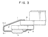
- a mounting system using a film carrier which is folded in one or more places is employed with the aim of producing as thin and as compact mounting as possible. This is illustrated, for example in Fig. 3 of the accompanying drawings.
- numeral 1 refers to an organic insulating film made of a polyimide, a polyester or the like; numeral 2 to a lead of a patterned electrical conductor formed from a conductive metal foil (such as a copper foil or a copper-based alloy foil) by photolithographic technology; numeral 3 to a moulded portion wherein a large scale integrated circuit (LSI) device is sealed with a resin; numeral 4 to an outer lead hole; numerals 5-1 and 5-2 to slits for folding (hereinafter often referred to as "folding slits"); numeral 8 to a liquid crystal panel; and numeral 9 to a panel circuit board.
- LSI large scale integrated circuit
- leads of the film carrier on the side of which the lead width and the lead pitch are relatively larger are soldered to the terminal area of the panel circuit board 9, while the leads of the film carrier on the side on which the lead width and the lead pitch are relatively smaller are bonded to the finely pitched connecting terminals on the liquid crystal panel 8 under heat and pressure by using an anisotropic conductive film or the like therebetween.
- the film carrier is folded in one or more places thereof, as shown in Fig. 3, to produce as thin and as compact mounting as possible.
- Fig. 4 of the accompanying drawings shows the structure of a conventional film carrier which is used, folded in one or more places, in mounting; while Fig. 5A is a cross section along line A-A of Fig. 4.
- numeral 1 refers to an organic insulating film made of a polyimide, a polyester or the like; numeral 2 to a patterned electrical conductor formed from a foil of an electrical conductor metal (such as copper or a copper-based alloy) by photolithographic technology; numeral 3 to a moulded portion wherein a large scale integrated circuit (LSI) device is sealed with a resin; numeral 4 to an outer lead hole; numerals 5-1 and 5-2 to folding slits; and numeral 6 to sprocket holes.
- This type of film carrier is used in mounting after having been cut along a cut line 7 to be separated from the organic insulating film.
- a film carrier as shown in Fig. 5A involves the grave problem that the yield thereof is lowered because disconnections, short circuits, etc. of leads are liable to occur in the course of production of film carriers, fitting of large scale integrated circuit (LSI) devices onto the film carriers, and folding of the film carriers in mounting.
- LSI large scale integrated circuit
- a film carrier as shown in Fig. 5B involves grave problems in that: (1) difficulty is encountered in mounting at a high density because the folding places thereof are not fixed) and (2) that residual stresses are generated in the folded places of the film carrier in mounting thereof to reduce the long-term reliability of connection portions.
- an object of the present invention is to provide a film carrier comprising an organic insulating film and a patterned electrical conductor adhered to the organic insulating film tape, wherein the foregoing problems of the prior art arising in keeping with the trend toward finer lead pitches can be solved by reducing the thickness of the organic insulating film tape in part(s) of the conductor pattern area thereof as compared with the thickness of the organic insulating film in the area thereof than the above-mentioned part(s) surrounded thereby.
- a film carrier comprising an organic insulating film tape having a patterned conductor adhered thereto, which carrier is provided with one or more folded places in one or more parts of the conductor pattern area, where the organic insulating film tape is smaller in thickness than in the area thereof other than the above-mentioned one or more parts surrounded thereby.
- the part(s) of the organic insulating film tape is preferably in the form, in plan, of a strip disposed perpendicular to or parallel with the longer direction of the film tape.
- the reduced thickness of the organic insulating film tape is suitably 4/5 to 1/10 of the larger thickness of the organic insulating film in the area other than the above-mentioned reduced thickness part(s).
- the number of folding places is preferably 1 to 5.
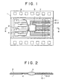
- Fig. 1 is a plan view of an example of a film carrier of the present invention, while Fig. 2 is a cross-section along line A-A of Fig. 1.
- numeral 1 refers to an organic insulating film made of a polyimide, a polyester or the like, which may be adhered to a copper foil, a copper-based alloy foil or the like; numeral 2 to a patterned electrical conductor formed from a foil of an electrical conductor metal (such as copper or a copper-based alloy) by photolithographic technology; numeral 3 to a moulded portion wherein a large scale integrated circuit (LSI) device is sealed with a resin; numeral 4 to an outer lead hole; and numeral 6 to sprocket holes.
- This film carrier is used in mounting thereof after having been cut along cut line 7 to be separated from the organic insulating film.
- the parts 10-1 and 10-2 of the organic insulating film of the film carrier which correspond to folding slits in the conventional film carrier, are smaller in film thickness than the area of the organic insulating film other than parts 10-1 and 10-2, to allow the film carrier to be folded.
- Methods of reducing the thickness of the organic insulating film in the folding place(s) include processing methods such as (1) mechanical cutting, (2) laser cutting, (3) chemical etching, and (4) plasma etching.
- a film carrier which comprises the step of punching a laminate tape comprising a foil of an electrical conductor metal and an organic insulating film applied thereon by a coating method to form sprocket holes, the step of mechanically cutting the tape with a cutting machine or the like to form device holes, outer lead holes, folding slits, etc., and the step of forming electrical conductor patterns by photolithographic technology (this process is disclosed in Japanese Patent Application No.
- the amount of cutting in the thickness-wise direction of the film with the above-mentioned cutting machine only in the case of the folding slits is decreased so as to provide a smaller thickness in the parts of the film corresponding to the folding slits than the original thickness of the organic insulating film, whereby the film carrier of the present invention can be produced.
- substantially the same processing (partial removal of the organic insulating film in the thickness-wise direction thereof) as described above can be achieved by any one of the aforementioned processing methods. Additionally, the processing step may be carried out in any stage between the course of production of the film carrier and a step just before mounting thereof. Thus, the point of time when the processing is done should be construed as a factor in limiting the scope of the present invention.
- the reduced thickness of the organic insulating film in part(s) of the electrical conductor pattern area thereof than that in the area thereof other than the above-mentioned parts surrounded thereby provides the film carrier of the present invention with the following effects.
Applications Claiming Priority (2)
| Application Number | Priority Date | Filing Date | Title |
|---|---|---|---|
| JP263408/89 | 1989-10-09 | ||
| JP26340889A JPH03125444A (ja) | 1989-10-09 | 1989-10-09 | 改良されたフィルムキャリヤー |
Publications (2)
| Publication Number | Publication Date |
|---|---|
| EP0422828A1 true EP0422828A1 (de) | 1991-04-17 |
| EP0422828B1 EP0422828B1 (de) | 1994-03-16 |
Family
ID=17389087
Family Applications (1)
| Application Number | Title | Priority Date | Filing Date |
|---|---|---|---|
| EP19900310838 Revoked EP0422828B1 (de) | 1989-10-09 | 1990-10-03 | Folienträger |
Country Status (3)
| Country | Link |
|---|---|
| EP (1) | EP0422828B1 (de) |
| JP (1) | JPH03125444A (de) |
| DE (1) | DE69007412T2 (de) |
Cited By (4)
| Publication number | Priority date | Publication date | Assignee | Title |
|---|---|---|---|---|
| EP0460668A2 (de) * | 1990-06-07 | 1991-12-11 | Casio Computer Company Limited | Modul für integrierte Schaltungen mit Verbindungsanordnung |
| WO1993005636A1 (de) * | 1991-09-02 | 1993-03-18 | Siemens Nixdorf Informationssysteme Aktiengesellschaft | BANDFÖRMIGER HILFSTRÄGER ALS MONTAGEHILFE FÜR DIE ZEILENWEISE MONTAGE VON HALBLEITERCHIPS AUF EINER PAßLÄCHE EINES TRÄGERELEMENTES |
| DE4337921A1 (de) * | 1993-11-06 | 1995-05-11 | Manfred Dr Michalk | Kontaktlose Chipkarte mit Antennenspule und Verfahren zu ihrer Herstellung |
| EP0708414A3 (de) * | 1994-10-22 | 1997-10-22 | Manfred Michalk | Kontaktloser Datenträger und Verfahren zu seiner Herstellung |
Citations (6)
| Publication number | Priority date | Publication date | Assignee | Title |
|---|---|---|---|---|
| EP0066339A2 (de) * | 1981-05-22 | 1982-12-08 | North American Philips Corporation | Trägerband aus Polymerschaum für Chips |
| EP0022279B1 (de) * | 1979-07-04 | 1984-03-14 | BBC Aktiengesellschaft Brown, Boveri & Cie. | Verfahren zur Herstellung eines optisch transparenten und elektrisch leitfähigen Filmmusters |
| EP0112177A2 (de) * | 1982-12-17 | 1984-06-27 | Wright Line Of Canada Ltd. | Mehrschichtetikettenband |
| JPS60240151A (ja) * | 1984-05-14 | 1985-11-29 | Matsushita Electric Ind Co Ltd | フイルムキヤリアテ−プの製造方法 |
| EP0042987B1 (de) * | 1980-06-30 | 1989-03-08 | International Business Machines Corporation | Träger mit elektronischer Schaltung für Halbleiteranordnung |
| EP0337775A2 (de) * | 1988-04-12 | 1989-10-18 | Sharp Kabushiki Kaisha | Elektronische Vorrichtung |
Family Cites Families (1)
| Publication number | Priority date | Publication date | Assignee | Title |
|---|---|---|---|---|
| JPS5388157A (en) * | 1977-01-13 | 1978-08-03 | Matsushita Electric Ind Co Ltd | Printed circuit board |
-
1989
- 1989-10-09 JP JP26340889A patent/JPH03125444A/ja active Pending
-
1990
- 1990-10-03 EP EP19900310838 patent/EP0422828B1/de not_active Revoked
- 1990-10-03 DE DE1990607412 patent/DE69007412T2/de not_active Revoked
Patent Citations (6)
| Publication number | Priority date | Publication date | Assignee | Title |
|---|---|---|---|---|
| EP0022279B1 (de) * | 1979-07-04 | 1984-03-14 | BBC Aktiengesellschaft Brown, Boveri & Cie. | Verfahren zur Herstellung eines optisch transparenten und elektrisch leitfähigen Filmmusters |
| EP0042987B1 (de) * | 1980-06-30 | 1989-03-08 | International Business Machines Corporation | Träger mit elektronischer Schaltung für Halbleiteranordnung |
| EP0066339A2 (de) * | 1981-05-22 | 1982-12-08 | North American Philips Corporation | Trägerband aus Polymerschaum für Chips |
| EP0112177A2 (de) * | 1982-12-17 | 1984-06-27 | Wright Line Of Canada Ltd. | Mehrschichtetikettenband |
| JPS60240151A (ja) * | 1984-05-14 | 1985-11-29 | Matsushita Electric Ind Co Ltd | フイルムキヤリアテ−プの製造方法 |
| EP0337775A2 (de) * | 1988-04-12 | 1989-10-18 | Sharp Kabushiki Kaisha | Elektronische Vorrichtung |
Cited By (6)
| Publication number | Priority date | Publication date | Assignee | Title |
|---|---|---|---|---|
| EP0460668A2 (de) * | 1990-06-07 | 1991-12-11 | Casio Computer Company Limited | Modul für integrierte Schaltungen mit Verbindungsanordnung |
| EP0460668A3 (en) * | 1990-06-07 | 1992-05-27 | Casio Computer Company Limited | Ic module and a junction structure thereof |
| WO1993005636A1 (de) * | 1991-09-02 | 1993-03-18 | Siemens Nixdorf Informationssysteme Aktiengesellschaft | BANDFÖRMIGER HILFSTRÄGER ALS MONTAGEHILFE FÜR DIE ZEILENWEISE MONTAGE VON HALBLEITERCHIPS AUF EINER PAßLÄCHE EINES TRÄGERELEMENTES |
| DE4337921A1 (de) * | 1993-11-06 | 1995-05-11 | Manfred Dr Michalk | Kontaktlose Chipkarte mit Antennenspule und Verfahren zu ihrer Herstellung |
| DE4337921C2 (de) * | 1993-11-06 | 1998-09-03 | Ods Gmbh & Co Kg | Kontaktlose Chipkarte mit Antennenspule |
| EP0708414A3 (de) * | 1994-10-22 | 1997-10-22 | Manfred Michalk | Kontaktloser Datenträger und Verfahren zu seiner Herstellung |
Also Published As
| Publication number | Publication date |
|---|---|
| DE69007412T2 (de) | 1994-10-06 |
| DE69007412D1 (de) | 1994-04-21 |
| JPH03125444A (ja) | 1991-05-28 |
| EP0422828B1 (de) | 1994-03-16 |
Similar Documents
| Publication | Publication Date | Title |
|---|---|---|
| US6490168B1 (en) | Interconnection of circuit substrates on different planes in electronic module | |
| KR100399379B1 (ko) | 반도체 장치와 그의 제조 방법, 액정 모듈 및 그의 탑재방법 | |
| US4841633A (en) | Method of mounting electronic parts onto single-sided printed wiring board | |
| US5590465A (en) | Method of manufacturing connection terminals of flexible wiring pattern substrates | |
| US20060008970A1 (en) | Optimized plating process for multilayer printed circuit boards having edge connectors | |
| KR100955439B1 (ko) | 반도체 장치용 테이프 캐리어, 반도체 장치의 제조 방법,반도체 장치 및 반도체 모듈 장치 | |
| US5306874A (en) | Electrical interconnect and method of its manufacture | |
| US5109601A (en) | Method of marking a thin film package | |
| EP3430469B1 (de) | Flexible leiterplatte, arraysubstrat, herstellungsverfahren dafür und anzeigevorrichtung | |
| KR100413027B1 (ko) | 테이프 캐리어 패키지 및 테이프 캐리어 패키지의 제조방법 | |
| EP0422828B1 (de) | Folienträger | |
| JP3226959B2 (ja) | 多層フレキシブルプリント基板の製法 | |
| US4965700A (en) | Thin film package for mixed bonding of chips | |
| WO2006098863A1 (en) | A 2-metal flex circuit and a method of manufacturing the same | |
| US5219607A (en) | Method of manufacturing printed circuit board | |
| JPH0685425A (ja) | 電子部品搭載用基板 | |
| US20030031001A1 (en) | Flat panel display and printed circuit board used therein | |
| JP2000091722A (ja) | プリント配線板及びその製造方法 | |
| WO2005027221A1 (en) | Chip on flex tape with dimension retention pattern | |
| JPH1093213A (ja) | 回路基板、回路装置および装置 | |
| JP2003142535A (ja) | フレキシブル配線基板およびその製造方法 | |
| JP3263863B2 (ja) | ハイブリッドic用基板とこれを用いたハイブリッドicの製造方法 | |
| JP3409380B2 (ja) | プリント基板装置 | |
| US6197208B1 (en) | Method for metallizing at least one printed circuit board or at least one pressed screen and at least one hybrid | |
| JP2580607B2 (ja) | 回路基板及び回路基板の製造方法 |
Legal Events
| Date | Code | Title | Description |
|---|---|---|---|
| PUAI | Public reference made under article 153(3) epc to a published international application that has entered the european phase |
Free format text: ORIGINAL CODE: 0009012 |
|
| AK | Designated contracting states |
Kind code of ref document: A1 Designated state(s): DE FR GB |
|
| 17P | Request for examination filed |
Effective date: 19910606 |
|
| 17Q | First examination report despatched |
Effective date: 19930625 |
|
| GRAA | (expected) grant |
Free format text: ORIGINAL CODE: 0009210 |
|
| AK | Designated contracting states |
Kind code of ref document: B1 Designated state(s): DE FR GB |
|
| REF | Corresponds to: |
Ref document number: 69007412 Country of ref document: DE Date of ref document: 19940421 |
|
| ET | Fr: translation filed | ||
| PLBE | No opposition filed within time limit |
Free format text: ORIGINAL CODE: 0009261 |
|
| PLAA | Information modified related to event that no opposition was filed |
Free format text: ORIGINAL CODE: 0009299DELT |
|
| PLBI | Opposition filed |
Free format text: ORIGINAL CODE: 0009260 |
|
| 26N | No opposition filed | ||
| 26 | Opposition filed |
Opponent name: VDO ADOLF SCHINDLING AG Effective date: 19941216 |
|
| PGFP | Annual fee paid to national office [announced via postgrant information from national office to epo] |
Ref country code: GB Payment date: 19960924 Year of fee payment: 7 |
|
| PGFP | Annual fee paid to national office [announced via postgrant information from national office to epo] |
Ref country code: FR Payment date: 19961009 Year of fee payment: 7 |
|
| PGFP | Annual fee paid to national office [announced via postgrant information from national office to epo] |
Ref country code: DE Payment date: 19961011 Year of fee payment: 7 |
|
| RDAH | Patent revoked |
Free format text: ORIGINAL CODE: EPIDOS REVO |
|
| RDAG | Patent revoked |
Free format text: ORIGINAL CODE: 0009271 |
|
| STAA | Information on the status of an ep patent application or granted ep patent |
Free format text: STATUS: PATENT REVOKED |
|
| 27W | Patent revoked |
Effective date: 19970218 |
|
| GBPR | Gb: patent revoked under art. 102 of the ep convention designating the uk as contracting state |
Free format text: 970218 |