EP0416478B1 - Procédé de fabrication d'un guide de lumière intégré - Google Patents
Procédé de fabrication d'un guide de lumière intégré Download PDFInfo
- Publication number
- EP0416478B1 EP0416478B1 EP90116736A EP90116736A EP0416478B1 EP 0416478 B1 EP0416478 B1 EP 0416478B1 EP 90116736 A EP90116736 A EP 90116736A EP 90116736 A EP90116736 A EP 90116736A EP 0416478 B1 EP0416478 B1 EP 0416478B1
- Authority
- EP
- European Patent Office
- Prior art keywords
- substrate
- groove
- optical waveguide
- optical
- electrodes
- Prior art date
- Legal status (The legal status is an assumption and is not a legal conclusion. Google has not performed a legal analysis and makes no representation as to the accuracy of the status listed.)
- Expired - Lifetime
Links
Images

Classifications
-
- G—PHYSICS
- G02—OPTICS
- G02F—OPTICAL DEVICES OR ARRANGEMENTS FOR THE CONTROL OF LIGHT BY MODIFICATION OF THE OPTICAL PROPERTIES OF THE MEDIA OF THE ELEMENTS INVOLVED THEREIN; NON-LINEAR OPTICS; FREQUENCY-CHANGING OF LIGHT; OPTICAL LOGIC ELEMENTS; OPTICAL ANALOGUE/DIGITAL CONVERTERS
- G02F1/00—Devices or arrangements for the control of the intensity, colour, phase, polarisation or direction of light arriving from an independent light source, e.g. switching, gating or modulating; Non-linear optics
- G02F1/01—Devices or arrangements for the control of the intensity, colour, phase, polarisation or direction of light arriving from an independent light source, e.g. switching, gating or modulating; Non-linear optics for the control of the intensity, phase, polarisation or colour
- G02F1/03—Devices or arrangements for the control of the intensity, colour, phase, polarisation or direction of light arriving from an independent light source, e.g. switching, gating or modulating; Non-linear optics for the control of the intensity, phase, polarisation or colour based on ceramics or electro-optical crystals, e.g. exhibiting Pockels effect or Kerr effect
- G02F1/035—Devices or arrangements for the control of the intensity, colour, phase, polarisation or direction of light arriving from an independent light source, e.g. switching, gating or modulating; Non-linear optics for the control of the intensity, phase, polarisation or colour based on ceramics or electro-optical crystals, e.g. exhibiting Pockels effect or Kerr effect in an optical waveguide structure
-
- G—PHYSICS
- G02—OPTICS
- G02F—OPTICAL DEVICES OR ARRANGEMENTS FOR THE CONTROL OF LIGHT BY MODIFICATION OF THE OPTICAL PROPERTIES OF THE MEDIA OF THE ELEMENTS INVOLVED THEREIN; NON-LINEAR OPTICS; FREQUENCY-CHANGING OF LIGHT; OPTICAL LOGIC ELEMENTS; OPTICAL ANALOGUE/DIGITAL CONVERTERS
- G02F1/00—Devices or arrangements for the control of the intensity, colour, phase, polarisation or direction of light arriving from an independent light source, e.g. switching, gating or modulating; Non-linear optics
- G02F1/01—Devices or arrangements for the control of the intensity, colour, phase, polarisation or direction of light arriving from an independent light source, e.g. switching, gating or modulating; Non-linear optics for the control of the intensity, phase, polarisation or colour
- G02F1/061—Devices or arrangements for the control of the intensity, colour, phase, polarisation or direction of light arriving from an independent light source, e.g. switching, gating or modulating; Non-linear optics for the control of the intensity, phase, polarisation or colour based on electro-optical organic material
- G02F1/065—Devices or arrangements for the control of the intensity, colour, phase, polarisation or direction of light arriving from an independent light source, e.g. switching, gating or modulating; Non-linear optics for the control of the intensity, phase, polarisation or colour based on electro-optical organic material in an optical waveguide structure
-
- G—PHYSICS
- G02—OPTICS
- G02F—OPTICAL DEVICES OR ARRANGEMENTS FOR THE CONTROL OF LIGHT BY MODIFICATION OF THE OPTICAL PROPERTIES OF THE MEDIA OF THE ELEMENTS INVOLVED THEREIN; NON-LINEAR OPTICS; FREQUENCY-CHANGING OF LIGHT; OPTICAL LOGIC ELEMENTS; OPTICAL ANALOGUE/DIGITAL CONVERTERS
- G02F1/00—Devices or arrangements for the control of the intensity, colour, phase, polarisation or direction of light arriving from an independent light source, e.g. switching, gating or modulating; Non-linear optics
- G02F1/01—Devices or arrangements for the control of the intensity, colour, phase, polarisation or direction of light arriving from an independent light source, e.g. switching, gating or modulating; Non-linear optics for the control of the intensity, phase, polarisation or colour
- G02F1/21—Devices or arrangements for the control of the intensity, colour, phase, polarisation or direction of light arriving from an independent light source, e.g. switching, gating or modulating; Non-linear optics for the control of the intensity, phase, polarisation or colour by interference
- G02F1/212—Mach-Zehnder type
-
- G—PHYSICS
- G02—OPTICS
- G02F—OPTICAL DEVICES OR ARRANGEMENTS FOR THE CONTROL OF LIGHT BY MODIFICATION OF THE OPTICAL PROPERTIES OF THE MEDIA OF THE ELEMENTS INVOLVED THEREIN; NON-LINEAR OPTICS; FREQUENCY-CHANGING OF LIGHT; OPTICAL LOGIC ELEMENTS; OPTICAL ANALOGUE/DIGITAL CONVERTERS
- G02F1/00—Devices or arrangements for the control of the intensity, colour, phase, polarisation or direction of light arriving from an independent light source, e.g. switching, gating or modulating; Non-linear optics
- G02F1/01—Devices or arrangements for the control of the intensity, colour, phase, polarisation or direction of light arriving from an independent light source, e.g. switching, gating or modulating; Non-linear optics for the control of the intensity, phase, polarisation or colour
- G02F1/21—Devices or arrangements for the control of the intensity, colour, phase, polarisation or direction of light arriving from an independent light source, e.g. switching, gating or modulating; Non-linear optics for the control of the intensity, phase, polarisation or colour by interference
- G02F1/225—Devices or arrangements for the control of the intensity, colour, phase, polarisation or direction of light arriving from an independent light source, e.g. switching, gating or modulating; Non-linear optics for the control of the intensity, phase, polarisation or colour by interference in an optical waveguide structure
Definitions
- the invention relates to a method for producing an optical waveguide which is integrated on a transparent substrate and has electrodes on its long sides.
- An arrangement is known from EP 0304602 A2 in which an optical waveguide is integrated on a substrate.
- the substrate has electro-optical properties, ie it shows the Pockels effect, and is preferably made from lithium niobate.
- an optical switch can be formed from them.
- a pair of electrodes is arranged above the surface of the substrate and separated from it by a dielectric intermediate layer.
- the small distance between the two optical fibers is dimensioned such that depending on the switching voltage between the optical fibers, light is coupled over.
- the optical waveguides are created by diffusing a material with a higher refractive index from the surface of the substrate in the areas provided for them.
- a disadvantage of this optical waveguide is that the required diffusion processes take place at high temperatures and the dimensions of the substrates are limited by the available lithium niobate single crystals.
- the lithium niobate material also has the disadvantage that its refractive index differs greatly from that of the glass of a glass fiber. Therefore, coupling losses occur when the light passes from a glass fiber optical waveguide to a lithium niobate optical waveguide.
- an optical component is known from DE 38 09 182 A1, in which an optical waveguide made of optically nonlinear material runs in a channel etched out of a Si substrate.
- the substrate is first covered with an SiO2 layer, which has a narrow opening at the point at which the channel is to be created.
- the Si substrate is etched below the opening, thus creating the hollow shape that forms the channel.
- an oxide layer must then be produced on the silicon within the channel by a tempering step at 1000 to 1200 ° C.
- the polymer must be pressed or sucked through the narrow opening into the much wider channel and the latter must be covered with a glass-like layer (SOG layer).
- SOG layer glass-like layer
- optical waveguides can be integrated in a variety of ways onto a substrate.
- the object is achieved in that the surface of the substrate is coated with a metal layer, in that the metal layer is then partially etched away in such a way that metallic strips are formed, so that the substrate is etched in the area between the strips, that a groove is formed, that the metallic strips are then etched away to those areas which are to form the electrodes, and that the groove is filled at least up to the level of the surface of these areas with a material which shows the electro-optical effect and forms the optical waveguide .
- the polymer provided here can also have higher electro-optical coefficients than lithium niobate.
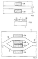
- a transparent substrate 1 (FIG. 1) is vapor-deposited with a metal layer 2 made of chrome and gold.
- the metal layer 2 (FIG. 2) is then structured photolithographically so that two metallic strips 21, 22 are formed from it.
- the gap remaining between the strips typically has a width of 10 »m and a length of 10-20 mm.
- the substrate 1 (FIG. 3) is removed from its surface in the area of the gap by an etching solution; the strips 21, 22 serve as an etching mask.
- There is a groove 3, the z. B. has a depth of 2 »m.
- the groove 3 is wider than the gap existing between the strips 21, 22 because the strips are under-etched by the etching solution. Therefore in a next step (FIG. 4), the gap is widened by etching off the strips, for example in a further photolithographic process, so that the strips 21, 22 no longer protrude beyond the groove 3.
- the regions 210, 220 (FIG. 5) which form the electrodes are produced from the strips 21, 22 by photolithography.
- Fig. 5 shows a top view.
- the substrate 1 (FIG. 6) is covered with a layer 4 made of a material which has electro-optical properties.
- Such a polymer consists, for. B. from polymethyl methacrylate and a solution or chemically bound azo or stilbene compound.
- the polymer has a higher refractive index than the substrate 1, so that the light is guided in the optical waveguide formed by the groove 3.
- the polymer is polarized by a DC voltage above its softening point and then cooled in an electric field. This gives it its electro-optical properties, e.g. that the refractive index of the optical fiber between the electrodes can be controlled by applying a voltage.
- the optical waveguide forms a phase modulator at this point.
- optical components e.g. B. integrate optical switches or directional couplers.
- a Mach-Zehnder interferometer (FIG. 7) consists, for example, of the groove 3, which branches into grooves 30, 31, which are brought together again to form a groove 32.
- the groove 31 has the areas 210, 220 as electrodes, the groove 30 corresponding areas 230, 240.
- the areas 210, 230 can also be combined into a single area.
Landscapes
- Physics & Mathematics (AREA)
- Nonlinear Science (AREA)
- General Physics & Mathematics (AREA)
- Optics & Photonics (AREA)
- Chemical & Material Sciences (AREA)
- Engineering & Computer Science (AREA)
- Ceramic Engineering (AREA)
- Crystallography & Structural Chemistry (AREA)
- Optical Integrated Circuits (AREA)
Claims (2)
- Processus de fabrication d'un guide d'ondes lumineuses intégré à la surface d'un substrat transparent (1) et présentant des électrodes (210, 220) sur ses grands côtés, caractérisé en ce que:- la surface du substrat (1) est revêtue d'une couche métallique (2),- la couche métallique est en partie corrodée de sorte qu'il apparaît des bandes métalliques (21, 22),- le substrat de la zone située entre les bandes est corrodé de telle sorte qu'il apparaît une rainure (3),- les bandes métalliques sont ensuite corrodées à l'exception des zones qui constituent les électrodes (210, 220), et- la rainure (3) est remplie, au moins jusqu'à hauteur de surface de ces zones, d'un matériau présentant l'effet électrooptique et composant le guide d'ondes lumineuses.
- Processus selon la revendication 1,
caractérisé en ce que:
un polymère polarisé au-dessus de son point de ramollissement par une tension de courant continu et refroidi ensuite, est utilisé comme matériau.
Applications Claiming Priority (2)
| Application Number | Priority Date | Filing Date | Title |
|---|---|---|---|
| DE3929410A DE3929410A1 (de) | 1989-09-05 | 1989-09-05 | Integrierter lichtwellenleiter |
| DE3929410 | 1989-09-05 |
Publications (3)
| Publication Number | Publication Date |
|---|---|
| EP0416478A2 EP0416478A2 (fr) | 1991-03-13 |
| EP0416478A3 EP0416478A3 (en) | 1992-03-11 |
| EP0416478B1 true EP0416478B1 (fr) | 1995-04-26 |
Family
ID=6388643
Family Applications (1)
| Application Number | Title | Priority Date | Filing Date |
|---|---|---|---|
| EP90116736A Expired - Lifetime EP0416478B1 (fr) | 1989-09-05 | 1990-08-31 | Procédé de fabrication d'un guide de lumière intégré |
Country Status (4)
| Country | Link |
|---|---|
| US (1) | US5069517A (fr) |
| EP (1) | EP0416478B1 (fr) |
| JP (1) | JP2721030B2 (fr) |
| DE (2) | DE3929410A1 (fr) |
Families Citing this family (13)
| Publication number | Priority date | Publication date | Assignee | Title |
|---|---|---|---|---|
| JPH04110831A (ja) * | 1990-08-31 | 1992-04-13 | Nec Corp | 光制御デバイス |
| EP0522637A3 (en) * | 1991-07-10 | 1993-08-04 | N.V. Philips' Gloeilampenfabrieken | Planar optical element |
| DE69217318T2 (de) * | 1991-10-08 | 1997-07-31 | Philips Electronics Nv | Optoelektronische Halbleiteranordnung mit einem Strahlungsleiter und Verfahren zum Herstellen einer derartigen Anordnung |
| DE19755402C2 (de) * | 1997-12-12 | 1999-11-11 | Litef Gmbh | Wellenlängenmeßeinrichtung mit mittelwertfrei angesteuertem Mach-Zehnder-Interferometer |
| DE10015830A1 (de) * | 2000-03-30 | 2001-10-11 | Fraunhofer Ges Forschung | Optischer Wellenleiter und Verfahren zum Herstellen desselben |
| US6760493B2 (en) * | 2001-06-28 | 2004-07-06 | Avanex Corporation | Coplanar integrated optical waveguide electro-optical modulator |
| GB2383424B (en) * | 2001-11-30 | 2004-12-22 | Marconi Optical Components Ltd | Photonic integrated device |
| US7343059B2 (en) * | 2003-10-11 | 2008-03-11 | Hewlett-Packard Development Company, L.P. | Photonic interconnect system |
| GB2407648B (en) * | 2003-10-31 | 2006-10-25 | Bookham Technology Plc | Polarisation rotators |
| US7231102B2 (en) * | 2004-01-16 | 2007-06-12 | Optimer Photonics, Inc. | Electrooptic modulator employing DC coupled electrodes |
| US20060216696A1 (en) * | 2004-08-23 | 2006-09-28 | Goguen Jon D | Rapid plague detection system |
| KR100785766B1 (ko) | 2005-10-13 | 2007-12-18 | 한국전자통신연구원 | 전기광학 효과를 이용한 광도파로 소자 및 그 소자를채용한 광학 기기 |
| JP7263966B2 (ja) * | 2019-08-02 | 2023-04-25 | 富士通オプティカルコンポーネンツ株式会社 | 光デバイス |
Family Cites Families (9)
| Publication number | Priority date | Publication date | Assignee | Title |
|---|---|---|---|---|
| FR2299662A1 (fr) * | 1974-06-14 | 1976-08-27 | Thomson Csf | Commutateur electro-optique et procede de fabrication d'un tel commutateur |
| US4445751A (en) * | 1981-10-19 | 1984-05-01 | Westinghouse Electric Corp. | Metal coated, tapered, optical fiber coupled to substrate and method of fabrication |
| US4474429A (en) * | 1982-03-04 | 1984-10-02 | Westinghouse Electric Corp. | Affixing an optical fiber to an optical device |
| JPS6037505A (ja) * | 1983-08-11 | 1985-02-26 | Nippon Telegr & Teleph Corp <Ntt> | 有機結晶を用いた光導波路の作製方法 |
| CA1278421C (fr) * | 1985-09-16 | 1991-01-02 | Salvatore Joseph Lalama | Materiaux et dispositifs optiques non-lineaires |
| JP2582066B2 (ja) * | 1987-03-19 | 1997-02-19 | 株式会社日立製作所 | 光機能性デバイス |
| US4768848A (en) * | 1987-05-29 | 1988-09-06 | Westinghouse Electric Corp. | Fiber optic repeater |
| US4871223A (en) * | 1987-08-25 | 1989-10-03 | Siemens Aktiengesellschaft | Arrangement comprising at least one integrated optical waveguide on a substrate of electro-optical material and comprising at least one electrode |
| US4936645A (en) * | 1989-08-24 | 1990-06-26 | Hoechst Celanese Corp. | Waveguide electrooptic light modulator with low optical loss |
-
1989
- 1989-09-05 DE DE3929410A patent/DE3929410A1/de not_active Withdrawn
-
1990
- 1990-08-31 DE DE59008958T patent/DE59008958D1/de not_active Expired - Fee Related
- 1990-08-31 EP EP90116736A patent/EP0416478B1/fr not_active Expired - Lifetime
- 1990-09-05 US US07/578,092 patent/US5069517A/en not_active Expired - Fee Related
- 1990-09-05 JP JP2235463A patent/JP2721030B2/ja not_active Expired - Fee Related
Non-Patent Citations (2)
| Title |
|---|
| Applied Physics Letters, Vol.20, No.6, 15 March 1972, pp.213-215, R.Ulrich et al.: "Embossed Optical Waveguides". * |
| Journal of Molecular Electronics, Vol.1 (1985), pp.25-45; J.Zyss "Nonlinear Organic Materials for Integrated Optics: A Review". * |
Also Published As
| Publication number | Publication date |
|---|---|
| DE3929410A1 (de) | 1991-03-07 |
| JP2721030B2 (ja) | 1998-03-04 |
| EP0416478A3 (en) | 1992-03-11 |
| EP0416478A2 (fr) | 1991-03-13 |
| JPH03100515A (ja) | 1991-04-25 |
| US5069517A (en) | 1991-12-03 |
| DE59008958D1 (de) | 1995-06-01 |
Similar Documents
| Publication | Publication Date | Title |
|---|---|---|
| EP0416478B1 (fr) | Procédé de fabrication d'un guide de lumière intégré | |
| DE60133498T2 (de) | Optischer Wanderwellenmodulator | |
| DE3809182C2 (de) | Optisches Bauelement mit organischem nicht-linearen Material | |
| EP1008013B1 (fr) | Commutateur thermo-optique | |
| EP0415225A2 (fr) | Dispositif optique intégré avec au moins un guide optique intégré sur un substrat semi-conducteur | |
| EP0306604A1 (fr) | Dispositif de réglage optique pour la régulation de rayons dans un guide optique, en particulier un commutateur optique | |
| DE60021996T2 (de) | Optischer Wanderwellenmodulator und Verfahren zu seiner Herstellung | |
| EP0037006B1 (fr) | Coupleur-étoile optique avec dispositif mélangeur planaire | |
| DE2704984A1 (de) | Schalter fuer lichtleitfasern | |
| EP0445527B1 (fr) | Composante optique de guide d'onde et méthode de fabrication d'une composante optique de guide d'onde | |
| EP0308602A2 (fr) | Guide d'ondes optiques enterré biréfringent ou structure de tels guides d'ondes et méthode pour la fabrication d'un tel guide d'ondes ou d'une telle structure | |
| DE10393740T5 (de) | Integrierte optische Vorrichtungen mit eingebetteten Elektroden sowie Verfahren zu ihrer Herstellung | |
| EP0837352B1 (fr) | Corps semi-conducteur, muni d'un élement de chauffage, pour la modulation de la lumière | |
| EP0831343B1 (fr) | Guide d'ondes optique et son procédé de fabrication | |
| DE3817035C1 (en) | Micromechanical switch for optical fibres | |
| DE19638099A1 (de) | Optischer Schalter | |
| EP0589902B1 (fr) | Circuit optique integre | |
| DE3024104A1 (de) | Integrierte mikrooptische vorrichtung zur verwendung mit multimode-lichtleitfasern und verfahren zu ihrer herstellung | |
| DE19508025A1 (de) | Verfahren zur Herstellung eines elektrooptischen Bauelements | |
| DE3724634C2 (de) | Elektro-optisches Bauelement | |
| DE10101119B4 (de) | Mechanisch stabile Anordnung mit mindestens einem photonischen Kristall und Verfahren zu deren Herstellung | |
| DE4202039C2 (de) | Verfahren zur Herstellung optoelektronischer Bauelemente | |
| EP0915511B1 (fr) | Dispositif comportant un substrat ayant une couche destinée a être chauffée | |
| DE4034382C1 (fr) | ||
| DD272519A1 (de) | Verfahren zur herstellung integriert elektrooptischer bauelemente |
Legal Events
| Date | Code | Title | Description |
|---|---|---|---|
| PUAI | Public reference made under article 153(3) epc to a published international application that has entered the european phase |
Free format text: ORIGINAL CODE: 0009012 |
|
| AK | Designated contracting states |
Kind code of ref document: A2 Designated state(s): DE FR GB NL SE |
|
| PUAL | Search report despatched |
Free format text: ORIGINAL CODE: 0009013 |
|
| AK | Designated contracting states |
Kind code of ref document: A3 Designated state(s): DE FR GB NL SE |
|
| 17P | Request for examination filed |
Effective date: 19920819 |
|
| RAP3 | Party data changed (applicant data changed or rights of an application transferred) |
Owner name: ALCATEL SEL AKTIENGESELLSCHAFT Owner name: ALCATEL N.V. |
|
| 17Q | First examination report despatched |
Effective date: 19940303 |
|
| GRAA | (expected) grant |
Free format text: ORIGINAL CODE: 0009210 |
|
| AK | Designated contracting states |
Kind code of ref document: B1 Designated state(s): DE FR GB NL SE |
|
| REF | Corresponds to: |
Ref document number: 59008958 Country of ref document: DE Date of ref document: 19950601 |
|
| GBT | Gb: translation of ep patent filed (gb section 77(6)(a)/1977) |
Effective date: 19950515 |
|
| ET | Fr: translation filed | ||
| PLBE | No opposition filed within time limit |
Free format text: ORIGINAL CODE: 0009261 |
|
| STAA | Information on the status of an ep patent application or granted ep patent |
Free format text: STATUS: NO OPPOSITION FILED WITHIN TIME LIMIT |
|
| 26N | No opposition filed | ||
| REG | Reference to a national code |
Ref country code: GB Ref legal event code: IF02 |
|
| PGFP | Annual fee paid to national office [announced via postgrant information from national office to epo] |
Ref country code: NL Payment date: 20020725 Year of fee payment: 13 Ref country code: SE Payment date: 20020725 Year of fee payment: 13 |
|
| PGFP | Annual fee paid to national office [announced via postgrant information from national office to epo] |
Ref country code: GB Payment date: 20020730 Year of fee payment: 13 |
|
| PGFP | Annual fee paid to national office [announced via postgrant information from national office to epo] |
Ref country code: DE Payment date: 20020809 Year of fee payment: 13 |
|
| PGFP | Annual fee paid to national office [announced via postgrant information from national office to epo] |
Ref country code: FR Payment date: 20020812 Year of fee payment: 13 |
|
| PG25 | Lapsed in a contracting state [announced via postgrant information from national office to epo] |
Ref country code: GB Free format text: LAPSE BECAUSE OF NON-PAYMENT OF DUE FEES Effective date: 20030831 |
|
| PG25 | Lapsed in a contracting state [announced via postgrant information from national office to epo] |
Ref country code: SE Free format text: LAPSE BECAUSE OF NON-PAYMENT OF DUE FEES Effective date: 20030901 |
|
| PG25 | Lapsed in a contracting state [announced via postgrant information from national office to epo] |
Ref country code: NL Free format text: LAPSE BECAUSE OF NON-PAYMENT OF DUE FEES Effective date: 20040301 |
|
| PG25 | Lapsed in a contracting state [announced via postgrant information from national office to epo] |
Ref country code: DE Free format text: LAPSE BECAUSE OF NON-PAYMENT OF DUE FEES Effective date: 20040302 |
|
| GBPC | Gb: european patent ceased through non-payment of renewal fee | ||
| PG25 | Lapsed in a contracting state [announced via postgrant information from national office to epo] |
Ref country code: FR Free format text: LAPSE BECAUSE OF NON-PAYMENT OF DUE FEES Effective date: 20040430 |
|
| NLV4 | Nl: lapsed or anulled due to non-payment of the annual fee |
Effective date: 20040301 |
|
| EUG | Se: european patent has lapsed | ||
| REG | Reference to a national code |
Ref country code: FR Ref legal event code: ST |