EP0415186A1 - Schaltungsanordnung zur Digital/Analog-Wandlung - Google Patents
Schaltungsanordnung zur Digital/Analog-Wandlung Download PDFInfo
- Publication number
- EP0415186A1 EP0415186A1 EP90115664A EP90115664A EP0415186A1 EP 0415186 A1 EP0415186 A1 EP 0415186A1 EP 90115664 A EP90115664 A EP 90115664A EP 90115664 A EP90115664 A EP 90115664A EP 0415186 A1 EP0415186 A1 EP 0415186A1
- Authority
- EP
- European Patent Office
- Prior art keywords
- digital
- analog converter
- analog
- output
- output signals
- Prior art date
- Legal status (The legal status is an assumption and is not a legal conclusion. Google has not performed a legal analysis and makes no representation as to the accuracy of the status listed.)
- Ceased
Links
- 238000006243 chemical reaction Methods 0.000 claims abstract description 5
- 230000005236 sound signal Effects 0.000 claims abstract description 3
- 101100015484 Saccharomyces cerevisiae (strain ATCC 204508 / S288c) GPA1 gene Proteins 0.000 claims description 9
- 230000008878 coupling Effects 0.000 claims description 6
- 238000010168 coupling process Methods 0.000 claims description 6
- 238000005859 coupling reaction Methods 0.000 claims description 6
- 239000003990 capacitor Substances 0.000 claims description 5
- 238000005070 sampling Methods 0.000 claims 1
- 101100067427 Saccharomyces cerevisiae (strain ATCC 204508 / S288c) FUS3 gene Proteins 0.000 description 6
- 230000000295 complement effect Effects 0.000 description 3
- 101100115778 Caenorhabditis elegans dac-1 gene Proteins 0.000 description 2
- 230000005540 biological transmission Effects 0.000 description 2
- 238000010586 diagram Methods 0.000 description 2
- 238000000034 method Methods 0.000 description 2
- 230000001105 regulatory effect Effects 0.000 description 2
- 230000008901 benefit Effects 0.000 description 1
- 230000008859 change Effects 0.000 description 1
- 238000011161 development Methods 0.000 description 1
- 230000018109 developmental process Effects 0.000 description 1
- 230000008569 process Effects 0.000 description 1
Images


Classifications
-
- H—ELECTRICITY
- H03—ELECTRONIC CIRCUITRY
- H03M—CODING; DECODING; CODE CONVERSION IN GENERAL
- H03M1/00—Analogue/digital conversion; Digital/analogue conversion
- H03M1/10—Calibration or testing
- H03M1/1009—Calibration
- H03M1/1033—Calibration over the full range of the converter, e.g. for correcting differential non-linearity
- H03M1/1038—Calibration over the full range of the converter, e.g. for correcting differential non-linearity by storing corrected or correction values in one or more digital look-up tables
-
- H—ELECTRICITY
- H03—ELECTRONIC CIRCUITRY
- H03M—CODING; DECODING; CODE CONVERSION IN GENERAL
- H03M1/00—Analogue/digital conversion; Digital/analogue conversion
- H03M1/06—Continuously compensating for, or preventing, undesired influence of physical parameters
- H03M1/0617—Continuously compensating for, or preventing, undesired influence of physical parameters characterised by the use of methods or means not specific to a particular type of detrimental influence
- H03M1/0675—Continuously compensating for, or preventing, undesired influence of physical parameters characterised by the use of methods or means not specific to a particular type of detrimental influence using redundancy
- H03M1/069—Continuously compensating for, or preventing, undesired influence of physical parameters characterised by the use of methods or means not specific to a particular type of detrimental influence using redundancy by range overlap between successive stages or steps
-
- H—ELECTRICITY
- H03—ELECTRONIC CIRCUITRY
- H03M—CODING; DECODING; CODE CONVERSION IN GENERAL
- H03M1/00—Analogue/digital conversion; Digital/analogue conversion
- H03M1/66—Digital/analogue converters
- H03M1/68—Digital/analogue converters with conversions of different sensitivity, i.e. one conversion relating to the more significant digital bits and another conversion to the less significant bits
Definitions
- the invention relates to a circuit arrangement for digital / analog conversion according to the preamble of the main claim.
- the object of the present invention is to provide a circuit arrangement for digital / analog conversion of high resolution, in particular for audio signals, in which simple digital / analog converter with lower resolution can be used.
- the circuit arrangement according to the invention with the characterizing features of the main claim has the advantage that a high amplitude resolution is obtained by interconnecting several digital / analog converters of lower resolution without inconsistencies in the analog output signal of the circuit arrangement according to the invention.
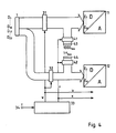
- a summing circuit 4 is provided for adding the output signals of the adding circuits AD2 to AD k and the digital / analog converter DAC1.
- a sample and hold circuit 5 is connected to the output of the summing circuit 4 and the output 6 of the analog signal is available.
- a converter operating mode and a compensation operating mode are provided.
- the digital / analog converters DAC1 to DAC k are supplied with the binary digits of the digital signal as follows:
- the digital / analog converter DAC1 receives the binary digits D1 to D N1
- the digital / analog converter DAC2 the binary digits D N1 + 1 to D N2
- the digital / analog converter DAC3 the binary digits D N2 + 1 to D N3 etc.
- the least significant digit of the inputs of the digital / analog converter DAC2 to DAC k is not addressed.
- the Adding circuits AD2 to AD k added a correction voltage to the amplified output voltages of the digital / analog converter DAC2 to DAC k .
- the size of these correction voltages is regulated in such a way that the output voltages of the individual digital / analog converters are matched to one another without jumps.
- the circuit arrangement according to FIG. 1 is switched into a compensation operating mode. This is done for a short time so that the operation as a digital / analog converter is not disturbed.
- the value 10 dans0 ⁇ 0 ⁇ hex and the digital / analog converter DAC2 the value 7F hex is supplied in the case of a two's complement representation of the digital signals to the digital / analog converter DAC1.
- the binary digits D1 to D N1-1 supplied to the digital / analog converter DAC1 are set to 0, while the binary digit D N1 receives the value 1.
- the correction voltage which is supplied to the adder circuit AD2, is regulated in such a way that the output voltages of the digital / analog converter DAC1 and the adder circuit 2 are the same.
- the DC voltage values of the digital / analog converter DAC3 to DAC k are adapted to the previous digital / analog converter.
- the binary digits of the digital signal are distributed to two digital / analog converters 11, 12 with the aid of a digital signal processor 10, which is programmed accordingly.
- the digital signal processor generates a signal K, which assumes the value 1 in the compensation mode, and a signal W, which is 1 in the converter mode.
- the analog output signals of the digital / analog converter 12 are amplified by a constant factor, for which purpose an amplifier 13 is provided, which is fed back by means of the resistors 14 and 15 in order to achieve a constant gain.
- the outputs of the amplifiers 13 and 16 are connected to the inputs of a further differential amplifier 19, to the output of which a storage capacitor 20 and the inverting input of the differential amplifier 16 are connected via an electronic switch 17.
- the signal K controls the switch 17 into the conductive state, so that the further differential amplifier 19 amplifies the difference between the output voltages of the amplifiers 13 and 16 and supplies it to the inverting input of the differential amplifier 16.
- a voltage is present at the capacitor 20 which brings about an adjustment of the output voltage of the differential amplifier 16 to that of the amplifier 13. This voltage is stored as a correction voltage for the subsequent converter operating mode, for which purpose the switch 17 is switched to the non-conductive state.
- the digital / analog converters each output an analog signal in accordance with the data at their inputs, the output signal of the Digital / analog converter 11 is corrected with the aid of the correction voltage. Both analog signals are then added in a summing circuit 21 and fed to a sample and hold circuit, which consists of a switch 22 and a capacitor 23.
- the switch 22 is closed during the converter mode so that the capacitor 23 can charge up to the sum of the analog signals generated by the converters and maintain the charge during the compensation mode.
- the analog signal can be taken off at the output 24 and used for further use.
- FIG. 3 shows an example of a coupling and control circuit which is used instead of the digital signal processor 10 (FIG. 2) for binary-coded signals can be used.
- the binary digits D1 to D16 are fed to a first bus driver 31, while a second bus driver 32 is provided for the binary digits D17 to D23.
- the bus driver 31 is connected to inputs E1 to E16 of the digital / analog converter 11, while the outputs of the bus driver 32 are connected to inputs E2 to E8 of the digital / analog converter 12.
- a control circuit 33 uses a clock signal T supplied at 34 to generate the signals W and K, which alternately assume the value 1 during a clock period of the clock signal T.
- the signal W controls the bus drivers 31, 32 into the conductive state, so that the digital signals are fed to the digital / analog converters as described.
- the bus drivers 31, 32 are blocked, while the signal K via two AND circuits 35, 36, a signal "1" the input E16 Digital / analog converter 11 and the input E1 of the digital / analog converter 12 supplies. The compensation as such takes place in the manner described in connection with FIG. 2.
- W and K each take the value 1 in succession during each clock period, that is to say that in addition to the converter operation, the correction voltage is derived during each clock period.
- the correction voltage can also be derived less frequently, since the errors to be compensated only change slowly. If there are more than two digital / analog converters, the adjustment is carried out one after the other in the direction of the digital / analog converter for the higher-order binary digits.
- Fig. 4 shows a coupling and control circuit in the case of a two's complement representation.
- the parts 31 to 34 have already been described in connection with FIG. 3.
- the values 10art0 ⁇ 0icillin hex and 7F hex are fed to the digital / analog converters 11, 12 in the compensation operating mode of inputs 43, 44.
- the adjustment can be carried out in one channel in each case if converter operation takes place in the other channel.
Landscapes
- Physics & Mathematics (AREA)
- Nonlinear Science (AREA)
- Engineering & Computer Science (AREA)
- Theoretical Computer Science (AREA)
- Analogue/Digital Conversion (AREA)
Applications Claiming Priority (2)
| Application Number | Priority Date | Filing Date | Title |
|---|---|---|---|
| DE19893928886 DE3928886A1 (de) | 1989-08-31 | 1989-08-31 | Schaltungsanordnung zur digital/analog-wandlung |
| DE3928886 | 1989-08-31 |
Publications (1)
| Publication Number | Publication Date |
|---|---|
| EP0415186A1 true EP0415186A1 (de) | 1991-03-06 |
Family
ID=6388321
Family Applications (1)
| Application Number | Title | Priority Date | Filing Date |
|---|---|---|---|
| EP90115664A Ceased EP0415186A1 (de) | 1989-08-31 | 1990-08-16 | Schaltungsanordnung zur Digital/Analog-Wandlung |
Country Status (2)
| Country | Link |
|---|---|
| EP (1) | EP0415186A1 (cg-RX-API-DMAC7.html) |
| DE (1) | DE3928886A1 (cg-RX-API-DMAC7.html) |
Citations (7)
| Publication number | Priority date | Publication date | Assignee | Title |
|---|---|---|---|---|
| US4677581A (en) * | 1985-05-30 | 1987-06-30 | Allied Corporation | Multichannel, self-calibrating, analog input/output apparatus for generating and measuring DC stimuli |
| US4680774A (en) * | 1985-02-13 | 1987-07-14 | Robert Bosch Gmbh | Method and circuit for suppression of quantitizing noise ambiguities |
| US4752767A (en) * | 1984-07-09 | 1988-06-21 | Hitachi, Ltd. | DA converter |
| GB2203305A (en) * | 1987-03-31 | 1988-10-12 | Mori Ryoichi | Digital to analog converter |
| US4843392A (en) * | 1985-05-03 | 1989-06-27 | Zdzislaw Gulczynski | Digital-to-analog converter with digital correction |
| GB2212367A (en) * | 1987-11-06 | 1989-07-19 | Int Computers Ltd | Window control using spare signal data bit |
| US4947172A (en) * | 1986-06-25 | 1990-08-07 | Kabushiki Kaisha Toshiba | Digital-to-analog conversion circuit |
Family Cites Families (1)
| Publication number | Priority date | Publication date | Assignee | Title |
|---|---|---|---|---|
| JPS57168522A (en) * | 1981-03-03 | 1982-10-16 | Intersil Inc | Digital-to-analog converter |
-
1989
- 1989-08-31 DE DE19893928886 patent/DE3928886A1/de active Granted
-
1990
- 1990-08-16 EP EP90115664A patent/EP0415186A1/de not_active Ceased
Patent Citations (7)
| Publication number | Priority date | Publication date | Assignee | Title |
|---|---|---|---|---|
| US4752767A (en) * | 1984-07-09 | 1988-06-21 | Hitachi, Ltd. | DA converter |
| US4680774A (en) * | 1985-02-13 | 1987-07-14 | Robert Bosch Gmbh | Method and circuit for suppression of quantitizing noise ambiguities |
| US4843392A (en) * | 1985-05-03 | 1989-06-27 | Zdzislaw Gulczynski | Digital-to-analog converter with digital correction |
| US4677581A (en) * | 1985-05-30 | 1987-06-30 | Allied Corporation | Multichannel, self-calibrating, analog input/output apparatus for generating and measuring DC stimuli |
| US4947172A (en) * | 1986-06-25 | 1990-08-07 | Kabushiki Kaisha Toshiba | Digital-to-analog conversion circuit |
| GB2203305A (en) * | 1987-03-31 | 1988-10-12 | Mori Ryoichi | Digital to analog converter |
| GB2212367A (en) * | 1987-11-06 | 1989-07-19 | Int Computers Ltd | Window control using spare signal data bit |
Also Published As
| Publication number | Publication date |
|---|---|
| DE3928886C2 (cg-RX-API-DMAC7.html) | 1991-10-17 |
| DE3928886A1 (de) | 1991-03-14 |
Similar Documents
| Publication | Publication Date | Title |
|---|---|---|
| DE69422046T2 (de) | Digital-analog-wandler mit überabtastung | |
| EP0707383B1 (de) | Schaltungsanordnung zur Analog-Digital-Wandlung von Signalen | |
| DE2823214A1 (de) | Schaltungsanordnung zur kompensierung des nullversatzes des ausgangssignals einer ein analogsignal verarbeitenden uebergeordneten anordnung | |
| DE19958049B4 (de) | Transkonduktor und Strommodus D/A-Wandler | |
| DE4221430B4 (de) | Bezugsspannungsschaltung mit schnellem Hochfahren der Leistung ausgehend von einem Bereitschaftszustand mit niedriger Leistung | |
| DE10020933B4 (de) | ASK-Modulator und Kommunikationsgerät mit einem ASK-Modulator | |
| DE3634979C2 (de) | Anordnung zur Erhöhung der Ausgangsleistung eines mit niedriger Spannung betriebenen Verstärkers, insbesondere für Autoradios | |
| EP0529119A1 (de) | Monolithisch integrierter Differenzverstärker mit digitaler Verstärkungseinstellung | |
| DE69029111T2 (de) | Seriell-Paralleler Analog/Digital Konverter | |
| DE10153309B4 (de) | Digital-Analog-Umsetzer-Vorrichtung mit hoher Auflösung | |
| DE2655508C3 (de) | Analogfiltersysteme | |
| DE2602382C2 (de) | Reihen-Parallel-Analog-Digital-Umsetzereinrichtung | |
| EP0261482B1 (de) | Operationsverstärker | |
| DE112021004609T5 (de) | Audio-schaltkreis, elektronisches gerät mit diesem schaltkreis und in einemfahrzeug eingebautes audiosystem | |
| EP0472555B1 (de) | D/a-wandler mit hoher linearität | |
| DE2553694C3 (de) | Ladungsgekoppelter Verstärker | |
| DE102012201711A1 (de) | Empfangsanordnung für ein Steuergerät in einem Fahrzeug und Verfahren zum Erzeugen eines Synchronisationspulses | |
| DE3147578A1 (de) | Analog/digital-wandler-schaltungsanordnung | |
| DE2337442A1 (de) | Verfahren und schaltungsanordnung zum kombinieren eines analogen signals mit einem digitalen signal | |
| DE69027889T2 (de) | Modulator | |
| DE2230597C3 (de) | Anordnung zur Erzeugung zweier zueinander hilberttransformierter Signale | |
| EP0217119A2 (de) | Verfahren zur Digital-Analog-Wandlung digitaler Informationen in bipolare Analogsignale | |
| DE3928886C2 (cg-RX-API-DMAC7.html) | ||
| DE3854535T2 (de) | Schaltung zur Kompensierung der Nichtlinearität der Ein-/Ausgangscharakteristik eines AD-Wandlers vom Parallel-Typ. | |
| DE3419645C2 (de) | Transversalfilter mit MOS-Transistor-Verstärkern |
Legal Events
| Date | Code | Title | Description |
|---|---|---|---|
| PUAI | Public reference made under article 153(3) epc to a published international application that has entered the european phase |
Free format text: ORIGINAL CODE: 0009012 |
|
| 17P | Request for examination filed |
Effective date: 19910102 |
|
| AK | Designated contracting states |
Kind code of ref document: A1 Designated state(s): DE FR GB IT SE |
|
| 17Q | First examination report despatched |
Effective date: 19930526 |
|
| STAA | Information on the status of an ep patent application or granted ep patent |
Free format text: STATUS: THE APPLICATION HAS BEEN REFUSED |
|
| 18R | Application refused |
Effective date: 19931112 |