EP0316616A2 - Analog-Digital-Umsetzer - Google Patents
Analog-Digital-Umsetzer Download PDFInfo
- Publication number
- EP0316616A2 EP0316616A2 EP88117681A EP88117681A EP0316616A2 EP 0316616 A2 EP0316616 A2 EP 0316616A2 EP 88117681 A EP88117681 A EP 88117681A EP 88117681 A EP88117681 A EP 88117681A EP 0316616 A2 EP0316616 A2 EP 0316616A2
- Authority
- EP
- European Patent Office
- Prior art keywords
- comparator
- analog
- constant
- switch
- input
- Prior art date
- Legal status (The legal status is an assumption and is not a legal conclusion. Google has not performed a legal analysis and makes no representation as to the accuracy of the status listed.)
- Granted
Links
- 239000003990 capacitor Substances 0.000 claims abstract description 34
- 239000008186 active pharmaceutical agent Substances 0.000 abstract description 2
- 238000000034 method Methods 0.000 description 7
- 238000005070 sampling Methods 0.000 description 2
- 238000006243 chemical reaction Methods 0.000 description 1
- 238000010586 diagram Methods 0.000 description 1
- 230000005669 field effect Effects 0.000 description 1
Images
Classifications
-
- H—ELECTRICITY
- H03—ELECTRONIC CIRCUITRY
- H03M—CODING; DECODING; CODE CONVERSION IN GENERAL
- H03M1/00—Analogue/digital conversion; Digital/analogue conversion
- H03M1/12—Analogue/digital converters
- H03M1/14—Conversion in steps with each step involving the same or a different conversion means and delivering more than one bit
- H03M1/16—Conversion in steps with each step involving the same or a different conversion means and delivering more than one bit with scale factor modification, i.e. by changing the amplification between the steps
- H03M1/162—Conversion in steps with each step involving the same or a different conversion means and delivering more than one bit with scale factor modification, i.e. by changing the amplification between the steps the steps being performed sequentially in a single stage, i.e. recirculation type
-
- H—ELECTRICITY
- H03—ELECTRONIC CIRCUITRY
- H03M—CODING; DECODING; CODE CONVERSION IN GENERAL
- H03M1/00—Analogue/digital conversion; Digital/analogue conversion
- H03M1/12—Analogue/digital converters
- H03M1/50—Analogue/digital converters with intermediate conversion to time interval
- H03M1/56—Input signal compared with linear ramp
Definitions
- the invention relates to an analog-to-digital converter according to the preamble of patent claim 1.
- Numerous methods are known for converting analog signals into digital signals.
- One of these methods is to discharge the storage capacitor of a sample and hold circuit with a constant current and to measure the length of time required to reach a predetermined potential. This time period is a direct measure of the sampled analog value.
- This method leads to more precise results if the storage capacitor is first discharged with a larger constant current up to a first threshold value and then with a constant fine current up to a second threshold value. With this circuit arrangement, the thresholds of a comparator have to be switched over.
- the storage capacitor must be relatively large in order to be able to work with constant currents of a suitable magnitude. However, this leads to non-linearities when sampling the analog signal.
- the object of the invention is to provide an analog-digital converter which operates according to the counting principle and has a high linearity.
- the storage capacitor of the sample and hold circuit must have a significantly lower capacitance, since it is no longer used by constant current sources to determine the size of the sample value must be unloaded. This task is carried out by the charging capacitor. It is also no longer necessary to apply different reference voltages to the comparator, since these are generated automatically by the different current paths of the constant currents.
- differential amplifiers are used as constant current sources, since this temperature can be dimensioned in a stable manner and at the same time assume the function of a switch.
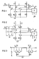
- a known analog-to-digital converter according to FIG. 1 contains a sample and hold circuit which consists of a first switch S1 and a storage capacitor C1.
- the output 2 of the sample and hold circuit is connected to a first input 3 of a comparator C0.
- a constant current source KG is connected to a supply potential -U and can be connected to the storage capacitor C1 via a second switch S2.
- a constant fine current source KF can be connected in the same way via a third switch S3.
- a voltage divider R1, R2 is connected to a second input 4 of the comparator C0 and lies between ground and the supply voltage -U.
- a third resistor R3 can be connected in parallel to the second resistor R2 of the voltage divider via a fourth switch S4.
- the switches S2 to S4 are actuated via a counting device ZE connected to the output 5 of the comparator C0.
- An analog signal AS is supplied to input 1 of the sample and hold circuit.
- a sample value is stored in the storage capacitor C1.
- the storage capacitor is then discharged via the second switch S2 with a constant current I G via the constant current source KG until the comparator output 5 emits a control signal SS which stops a counter of the counting device ZE.
- the length of time for the storage capacitor to be discharged is generally measured by supplying a digital clock with an operating cycle at a constant frequency.
- the control signal SS of the comparator also causes the second switch S2 to open and the fourth switch S4 and the third switch S3 to close.
- a (here more negative) comparison voltage U V is then present at the second input 4 of the comparator C0 and the storage capacitor C1 is then discharged with a low constant fine current I F from the constant fine current source KF and the end-of-charge time is measured again until the comparator C0 is switched on again at its output 5 Outputs control signal SS that stops the second counting process - for example, carried out with a second counter.
- a binary-coded data signal DS which was determined from both counting processes, is emitted at the outputs 6 of the counting device.
- the necessary control logic is assigned to the counting device, for example.
- the constant current sources can of course also be switched over or the switches S2 and S3 can be replaced by a changeover switch.
- the sample and hold circuit SH is connected directly to the first input 3 of the comparator C0.
- a series resistor RV is connected to a charging capacitor C2, the second connection of which is connected to ground.
- a second switch S2 is connected in parallel to the charging capacitor.
- a third switch S3 - shown in broken lines - can be connected in parallel to the storage capacitor C1.
- the constant current source KG can be connected directly to the second input 4 of the comparator C0 via a fourth switch S4.
- the constant fine current source KF can be connected directly to the charging capacitor C2 via a fifth switch S5. Both constant current sources are again connected to the supply potential -U.
- the fourth and fifth switches are in turn actuated by the counting device ZE or by a control logic assigned to them. Bipolar transistors or field effect transistors can be used as switches.
- the comparator If the voltage at the comparator inputs is the same (or if the voltage at the second input 4 has even become slightly more negative than that at the first input 3), the comparator outputs the control signal SS at output 5, which stops a counting process for measuring the discharge time, the fourth Switch S4 opens and directly connects it to the charging capacitor C2 via the fifth switch S5 of the constant fine current source KF. By opening the fourth switch S4, the potential at the second comparator input 4 is again positive and the charging capacitor is now discharged further with the constant fine current I F until there is again voltage equality at the comparator inputs and a second control signal SS at the comparator output makes a second count process for measuring the discharge time via the constant fine current source ended, whereby the analog-digital conversion has finally taken place.
- the capacitance of the storage capacitor C1 can be significantly smaller than that of the charging capacitor C2.
- the capacity ratio should be less than 1:10; however, it can also be 1: 100 or even less.
- the dimensioning depends on the sampling frequency and the internal resistance of the voltage source of the analog signal. In one dimensioning example, the capacitance of the storage capacitor is 100 pF and the capacitance of the charging capacitor is 10 nF. A high linearity is achieved due to the small capacitance of the sample and hold circuit.
- the switch S3 ensures that the storage capacitor C1 is always charged starting from the same potential. In general, it can be omitted.
- Each constant current source consists of a differential amplifier DV1 or DV2.
- Each input 11 (base connection) of a differential amplifier is connected to that of the other and is at a constant potential U K.
- the other amplifier inputs 7 and 8 are led out and are controlled by the corresponding outputs of the counting device.
- the constant current I G at the output 9 is determined by the common emitter resistance RK1 of the transistors of the first differential amplifier DV1 and the constant voltage U K.
- the common emitter resistor RK2 of the second differential amplifier DV2 is, for example, a factor 128 greater than the emitter resistor RK1. This results in a correspondingly lower constant fine current I F at the output 10 of the second differential amplifier DV2.
- the designations of the circuit points correspond to those of FIG. 2. Of course, numerous variants for the circuit arrangement and temperature compensation are also possible here.
Landscapes
- Engineering & Computer Science (AREA)
- Theoretical Computer Science (AREA)
- Analogue/Digital Conversion (AREA)
- Measurement Of Current Or Voltage (AREA)
- Emergency Protection Circuit Devices (AREA)
Abstract
Description
- Die Erfindung betrifft ein Analog-Digital-Umsetzer nach dem Oberbegriff des Patentanspruchs 1.
- Für die Umsetzung von analogen Signalen in digitale Signale sind zahlreiche Verfahren bekannt. Eines dieser Verfahren besteht darin, den Speicherkondensator einer Abtast- und Halteschaltung mit einem konstanten Strom zu entladen und die Zeitdauer zu messen, die benötigt wird, um ein vorgegebenes Potential zu erreichen. Diese Zeitdauer ist ein direktes Maß für den abgetasteten Analogwert. Dies Verfahren führt zu genaueren Ergebnissen, wenn die Entladung des Speicherkondensators zunächst mit einem größeren Konstantstrom bis zu einem ersten Schwellwert und anschließend mit einem konstanten Feinstrom bis zu einem zweiten Schwellwert erfolgt. Bei dieser Schaltungsanordnung müssen die Schwellen eines Komparators umgeschaltet werden. Der Speicherkondensator muß relativ groß sein, um noch mit Konstantströmen einer geeigneten Größenordnung arbeiten zu können. Dies führt jedoch zu Unlinearitäten beim Abtasten des Analogsignals.
- Aufgabe der Erfindung ist es, einen nach dem Zählprinzip arbeitenden Analog-Digital-Umsetzer mit hoher Linearität anzugeben.
- Diese Aufgabe wird durch die im Patentanspruch 1 angegebenen Merkmale gelöst. Vorteilhafte Ausbildungen sind in den Unteransprüchen angegeben.
- Vorteilhaft bei dieser Schaltungsanordnung ist es, daß der Speicherkondensator der Abtast- und Halteschaltung eine wesentlich geringere Kapazität aufweisen muß, da er nicht mehr durch Konstantstromquellen zur Feststellung der Größe des Abtastwertes entladen werden muß. Diese Aufgabe wird durch den Ladekondensator übernommen. Auch müssen an den Komparator keine unterschiedlichen Vergleichsspannungen mehr angelegt werden, da diese durch die unterschiedlichen Stromwege der Konstantströme automatisch erzeugt werden.
- Vorteilhaft ist auch, daß als Konstantstromquellen Differenzverstärker verwendet werden, da diese Temperatur stabil dimensioniert werden können um gleichzeitig die Funktion eines Schalters übernehmen.
- Ein Ausführungsbeispiel der Erfindung wird anhand von Figuren näher beschrieben.
- Es zeigen
- Fig. 1 einen bekannten Analog-Digital-Umsetzer,
- Fig. 2 einen erfindungsgemäßen Analog-Digital-Umsetzer und
- Fig. 3 ein Ausführungsbeispiel für die Konstantstromquellen.
- Ein bekannter Analog-Digital-Umsetzer nach Fig. 1 enthält eine Abtast- und Halteschaltung, die aus einem ersten Schalter S1 und einem Speicherkondensator C1 besteht. Der Ausgang 2 der Abtast- und Halteschaltung ist mit einem ersten Eingang 3 eines Komparators C0 verbunden. Eine Konstantstromquelle KG ist an ein Versorgungspotential -U angeschaltet und kann über einen zweiten Schalter S2 mit dem Speicherkondensator C1 verbunden werden. Eine Konstantfeinstromquelle KF ist in derselben Weise über einen dritten Schalter S3 anschaltbar. An einem zweiten Eingang 4 des Komparators C0 ist ein Spannungsteiler R1, R2 angeschaltet, der zwischen Masse und der Versorgungsspannung -U liegt. Über einen vierten Schalter S4 kann ein dritter Widerstand R3 zum zweiten Widerstand R2 des Spannungsteilers parallel geschaltet werden. Über eine an den Ausgang 5 des Komparators C0 angeschaltete Zähleinrichtung ZE werden die Schalter S2 bis S4 betätigt.
- Dem Eingang 1 der Abtast- und Halteschaltung wird ein Analogsignal AS zugeführt. Durch kurzzeitiges Schließen des ersten Schalters S1 wird ein Abtastwert in dem Speicherkondensator C1 gespeichert. Anschließend wird über den zweiten Schalter S2 der Speicherkondensator mit einem Konstantstrom IG über die Konstantstromquelle KG entladen, bis der Komparatorausgang 5 ein Steuersignal SS abgibt, das einen Zähler der Zähleinrichtung ZE stoppt. Die Zeitdauer für das Entladen des Speicherkondensators wird im allgemeinen gemessen, indem einem Digitalzähler ein Arbeitstakt mit konstanter Frequenz zugeführt wird. Das Steuersignal SS des Komparators bewirkt außerdem ein Öffnen des zweiten Schalters S2 und ein Schließen des vierten Schalters S4 und des dritten Schalters S3. Am zweiten Eingang 4 des Komparators C0 liegt dann eine (hier negativere) Vergleichsspannung UV an und der Speicherkondensator C1 wird anschließend mit einem geringen Konstantfeinstrom IF der Konstantfeinstromquelle KF entladen und die Endladezeit wieder gemessen, bis der Komparator C0 an seinem Ausgang 5 erneut ein Steuersignal SS abgibt, das den zweiten Zählvorgang - beispielsweise mit einem zweiten Zähler ausgeführt - stoppt. An den Ausgängen 6 der Zähleinrichtung wird ein binär codiertes Datensignal DS abgegeben, das aus beiden Zählvorgängen ermittelt wurde. Die notwendige Steuerlogik ist beispielsweise der Zähleinrichtung zugeordnet. Für die Erzeugung der Vergleichsspannungen UV sind natürlich die unterschiedlichsten Varianten denkbar. Ebenso können natürlich auch die Konstantstromquellen umgeschaltet werden oder die Schalter S2 und S3 durch einen Umschalter ersetzt werden.
- In Fig. 2 ist ein Ausführungsbeispiel des erfindungsgemäßen Analog-Digital-Umsetzers dargestellt. Die Abtast- und Halteschaltung SH ist direkt mit dem ersten Eingang 3 des Komparators C0 verbunden. An dem zweiten Eingang 4 des Komparators ist über einen Vorwiderstand RV ein Ladekondensator C2 angeschaltet, dessen zweiter Anschluß an Masse liegt. Parallel zum Ladekondensator liegt ein zweiter Schalter S2. Ein dritter Schalter S3 - strichliert eingezeichnet - kann parallel zum Speicherkondensator C1 geschaltet werden. Die Konstantstromquelle KG ist über einen vierten Schalter S4 direkt an den zweiten Eingang 4 des Komparators C0 anschaltbar. Die Konstantfeinstromquelle KF kann dagegen über einen fünften Schalter S5 direkt an den Ladekondensator C2 angeschaltet werden. Beide Konstantstromquellen sind wieder mit dem Versorgungspotential -U verbunden. Der vierte und der fünfte Schalter werden wiederum von der Zähleinrichtung ZE betätigt, bzw. von einer ihr zugeordneten Steuerlogik. Als Schalter können bipolare Transistoren oder Feldeffekttransistoren verwendet werden.
- Durch das Schließen des ersten Schalters S1 wird - wie in der bekannten Ausführungsform nach Fig. 1 - ein Abtastwert im Speicherkondensator C1 gespeichert. Gleichzeitig jedoch ist der Ladekondensator C2 durch kurzzeitiges Schließen des zweiten Schalters S2 entladen worden. Anschließend wird der Ladekondensator C2 durch Schließen des vierten Schalters S4 zunächst mit dem Konstantstrom IG entladen. Hierdurch wird ein Spannungsabfall am Vorwiderstand RV erzeugt, durch den das Potential am zweiten Eingang 4 des Komparators noch negativer wird. Bei Spannungsgleichheit an den Komparatoreingängen (bzw. wenn die Spannung am zweiten Eingang 4 sogar minimal negativer als die am ersten Eingang 3 geworden ist) gibt der Komparator am Ausgang 5 das Steuersignal SS ab, das wieder einen Zählvorgang zur Messung der Entladedauer stoppt, den vierten Schalter S4 öffnet und dafür über den fünften Schalter S5 der Konstantfeinstromquelle KF direkt an den Ladekondensator C2 anschaltet. Durch das Öffnen des vierten Schalters S4 wird das Potential am zweiten Komparatoreingang 4 wieder positiver und der Ladekondensator wird jetzt mit dem Konstantfeinstrom IF weiter entladen, bis erneut Spannungsgleichheit an den Komparatoreingängen herrscht und ein zweites Steuersignal SS am Komparatorausgang einen zweiten Zähl vorgang zur Messung der Entladedauer über die Konstantfeinstromquelle beendet, wodurch auch die Analog-Digital-Umsetzung endgültig erfolgt ist.
- Die Kapazität des Speicherkondensators C1 kann wesentlich kleiner als die des Ladekondensators C2 sein. Das Kapazitätsverhältnis sollte kleiner als 1:10 sein; es kann aber auch 1:100 betragen oder sogar noch darunter liegen. Die Dimensionierung ist abhängig von der Abtastfrequenz und vom Innenwiderstand der Spannungsquelle des Analogsignals. Bei einem Dimensionierungsbeispiel beträgt die Kapazität des Speicherkondensators 100 pF und die Kapazität des Ladekondensators 10 nF. Durch die geringe Kapazität der Abtast- und Halteschaltung wird eine hohe Linearität erreicht. Durch den Schalter S3 wird dafür gesorgt, daß der Speicherkondensator C1 stets vom selben Potential ausgehend aufgeladen wird. Im allgemeinen kann er entfallen.
- In Fig. 3 ist ein Prinzipschaltbild für die Konstantstromquellen dargestellt. Jede Konstantstromquelle besteht aus einem Differenzverstärker DV1 bzw. DV2. Jeweils ein Eingang 11 (Basisanschluß) eines Differenzverstärkers ist mit dem des anderen zusammengeschaltet und liegt an einem konstanten Potential UK an. Die anderen Verstärkereingänge 7 bzw. 8 sind herausgeführt und werden von den entsprechenden Ausgängen der Zähleinrichtung angesteuert. Durch den gemeinsamen Emitterwiderstand RK1 der Transistoren des ersten Differenzverstärkers DV1 und die konstante Spannung UK ist der Konstantstrom IG am Ausgang 9 festgelegt. Der gemeinsame Emitterwiderstand RK2 des zweiten Differenzverstärkers DV2 ist beispielsweise um den Faktor 128 größer als der Emitterwiderstand RK1. Hierdurch ergibt sich ein entsprechend geringerer Konstantfeinstrom IF am Ausgang 10 des zweiten Differenzverstärkers DV2. Die Bezeichnungen der Schaltungspunkte entspricht denen der Fig. 2. Natürlich sind auch hier zahlreiche Varianten für die Schaltungsanordnung und eine Temperaturenkompensation möglich.
Claims (4)
dadurch gekennzeichnet,
daß ein Ladekondensator (C2) über einen Vorwiderstand (RV) an einen zweiten Eingang (4) des Komparators (C0) angeschaltet ist,
daß die Konstantstromquelle (KG) ebenfalls an den zweiten Eingang (4) des Komparators (C0) anschaltbar ist,
daß die Konstantfeinstromquelle (KF) direkt an den Ladekondensator (C2) anschaltbar ist
und daß ein zweiter Schalter (S2) parallel zum Ladekondensator (C2) geschaltet ist.
dadurch gekennzeichnet,
daß ein dritter Schalter (S3) zu dem Speicherkondensator (C1) parallelgeschaltet ist.
dadurch gekennzeichnet,
daß als Konstantstromquelle (KG) und als Konstantfeinstromquelle (KF) Differenzverstärker (DV1, DV2) vorgesehen sind.
dadurch gekennzeichnet,
daß das Verhältnis der Kapazität des Speicherkondensators C1 zur Kapazität des Ladekondensators kleiner als 1:10 ist.
Applications Claiming Priority (2)
| Application Number | Priority Date | Filing Date | Title |
|---|---|---|---|
| DE3739209 | 1987-11-19 | ||
| DE3739209 | 1987-11-19 |
Publications (3)
| Publication Number | Publication Date |
|---|---|
| EP0316616A2 true EP0316616A2 (de) | 1989-05-24 |
| EP0316616A3 EP0316616A3 (de) | 1992-06-03 |
| EP0316616B1 EP0316616B1 (de) | 1995-03-29 |
Family
ID=6340802
Family Applications (1)
| Application Number | Title | Priority Date | Filing Date |
|---|---|---|---|
| EP88117681A Expired - Lifetime EP0316616B1 (de) | 1987-11-19 | 1988-10-24 | Analog-Digital-Umsetzer |
Country Status (5)
| Country | Link |
|---|---|
| EP (1) | EP0316616B1 (de) |
| AT (1) | ATE120587T1 (de) |
| DE (1) | DE3853461D1 (de) |
| ES (1) | ES2069540T3 (de) |
| NO (1) | NO885159L (de) |
Cited By (40)
| Publication number | Priority date | Publication date | Assignee | Title |
|---|---|---|---|---|
| US6075480A (en) * | 1998-10-23 | 2000-06-13 | Deliberis, Jr.; Romeo A. | Down range returns simulator |
| WO2003041278A1 (en) * | 2001-11-05 | 2003-05-15 | Cameron Health, Inc. | Low power a/d converter |
| US6778860B2 (en) | 2001-11-05 | 2004-08-17 | Cameron Health, Inc. | Switched capacitor defibrillation circuit |
| US6834204B2 (en) | 2001-11-05 | 2004-12-21 | Cameron Health, Inc. | Method and apparatus for inducing defibrillation in a patient using a T-shock waveform |
| US6856835B2 (en) | 2000-09-18 | 2005-02-15 | Cameron Health, Inc. | Biphasic waveform for anti-tachycardia pacing for a subcutaneous implantable cardioverter-defibrillator |
| US6865417B2 (en) | 2001-11-05 | 2005-03-08 | Cameron Health, Inc. | H-bridge with sensing circuit |
| US6866044B2 (en) | 2000-09-18 | 2005-03-15 | Cameron Health, Inc. | Method of insertion and implantation of implantable cardioverter-defibrillator canisters |
| US6952610B2 (en) | 2000-09-18 | 2005-10-04 | Cameron Health, Inc. | Current waveforms for anti-tachycardia pacing for a subcutaneous implantable cardioverter- defibrillator |
| US6952608B2 (en) | 2001-11-05 | 2005-10-04 | Cameron Health, Inc. | Defibrillation pacing circuitry |
| US6954670B2 (en) | 2001-11-05 | 2005-10-11 | Cameron Health, Inc. | Simplified defibrillator output circuit |
| US6988003B2 (en) | 2000-09-18 | 2006-01-17 | Cameron Health, Inc. | Implantable cardioverter-defibrillator having two spaced apart shocking electrodes on housing |
| US7039459B2 (en) | 2000-09-18 | 2006-05-02 | Cameron Health, Inc. | Cardioverter-defibrillator having a focused shocking area and orientation thereof |
| US7043299B2 (en) | 2000-09-18 | 2006-05-09 | Cameron Health, Inc. | Subcutaneous implantable cardioverter-defibrillator employing a telescoping lead |
| US7065410B2 (en) | 2000-09-18 | 2006-06-20 | Cameron Health, Inc. | Subcutaneous electrode with improved contact shape for transthorasic conduction |
| US7076296B2 (en) | 2000-09-18 | 2006-07-11 | Cameron Health, Inc. | Method of supplying energy to subcutaneous cardioverter-defibrillator and pacer |
| US7092754B2 (en) | 2000-09-18 | 2006-08-15 | Cameron Health, Inc. | Monophasic waveform for anti-bradycardia pacing for a subcutaneous implantable cardioverter-defibrillator |
| US7090682B2 (en) | 2000-09-18 | 2006-08-15 | Cameron Health, Inc. | Method and apparatus for extraction of a subcutaneous electrode |
| US7120495B2 (en) | 2000-09-18 | 2006-10-10 | Cameron Health, Inc. | Flexible subcutaneous implantable cardioverter-defibrillator |
| US7146212B2 (en) | 2000-09-18 | 2006-12-05 | Cameron Health, Inc. | Anti-bradycardia pacing for a subcutaneous implantable cardioverter-defibrillator |
| US7194309B2 (en) | 2000-09-18 | 2007-03-20 | Cameron Health, Inc. | Packaging technology for non-transvenous cardioverter/defibrillator devices |
| US7194302B2 (en) | 2000-09-18 | 2007-03-20 | Cameron Health, Inc. | Subcutaneous cardiac stimulator with small contact surface electrodes |
| US7655014B2 (en) | 2004-12-06 | 2010-02-02 | Cameron Health, Inc. | Apparatus and method for subcutaneous electrode insertion |
| US7657311B2 (en) | 2000-09-18 | 2010-02-02 | Cameron Health, Inc. | Subcutaneous only implantable cardioverter-defibrillator and optional pacer |
| US7751885B2 (en) | 2000-09-18 | 2010-07-06 | Cameron Health, Inc. | Bradycardia pacing in a subcutaneous device |
| US7877139B2 (en) | 2006-09-22 | 2011-01-25 | Cameron Health, Inc. | Method and device for implantable cardiac stimulus device lead impedance measurement |
| US7991459B2 (en) | 2004-11-29 | 2011-08-02 | Cameron Health, Inc. | Method for defining signal templates in implantable cardiac devices |
| US8014851B2 (en) | 2006-09-26 | 2011-09-06 | Cameron Health, Inc. | Signal analysis in implantable cardiac treatment devices |
| CN102195652A (zh) * | 2010-03-19 | 2011-09-21 | Nxp股份有限公司 | 采样保持放大器 |
| US8160697B2 (en) | 2005-01-25 | 2012-04-17 | Cameron Health, Inc. | Method for adapting charge initiation for an implantable cardioverter-defibrillator |
| US8229563B2 (en) | 2005-01-25 | 2012-07-24 | Cameron Health, Inc. | Devices for adapting charge initiation for an implantable cardioverter-defibrillator |
| US8626285B2 (en) | 2003-06-02 | 2014-01-07 | Cameron Health, Inc. | Method and devices for performing cardiac waveform appraisal |
| US8718793B2 (en) | 2006-08-01 | 2014-05-06 | Cameron Health, Inc. | Electrode insertion tools, lead assemblies, kits and methods for placement of cardiac device electrodes |
| US8781602B2 (en) | 2007-02-07 | 2014-07-15 | Cameron Health, Inc. | Sensing vector selection in a cardiac stimulus device with postural assessment |
| US8788023B2 (en) | 2006-05-26 | 2014-07-22 | Cameron Health, Inc. | Systems and methods for sensing vector selection in an implantable medical device |
| CN104052459A (zh) * | 2014-06-06 | 2014-09-17 | 华为技术有限公司 | 一种采样电路及采样方法 |
| US8942802B2 (en) | 2003-05-29 | 2015-01-27 | Cameron Health, Inc. | Method for discriminating between ventricular and supraventricular arrhythmias |
| US9138589B2 (en) | 2001-11-21 | 2015-09-22 | Cameron Health, Inc. | Apparatus and method for identifying atrial arrhythmia by far-field sensing |
| US9149645B2 (en) | 2013-03-11 | 2015-10-06 | Cameron Health, Inc. | Methods and devices implementing dual criteria for arrhythmia detection |
| CN105515584A (zh) * | 2016-01-12 | 2016-04-20 | 上海申矽凌微电子科技有限公司 | 检测电阻转换为数字的电路 |
| US9579065B2 (en) | 2013-03-12 | 2017-02-28 | Cameron Health Inc. | Cardiac signal vector selection with monophasic and biphasic shape consideration |
Families Citing this family (2)
| Publication number | Priority date | Publication date | Assignee | Title |
|---|---|---|---|---|
| US8116867B2 (en) | 2005-08-04 | 2012-02-14 | Cameron Health, Inc. | Methods and devices for tachyarrhythmia sensing and high-pass filter bypass |
| US7783340B2 (en) | 2007-01-16 | 2010-08-24 | Cameron Health, Inc. | Systems and methods for sensing vector selection in an implantable medical device using a polynomial approach |
Citations (3)
| Publication number | Priority date | Publication date | Assignee | Title |
|---|---|---|---|---|
| US3281828A (en) * | 1962-09-17 | 1966-10-25 | Nippon Electric Co | Encoder with non-linear quantization |
| US3778812A (en) * | 1971-03-17 | 1973-12-11 | Siemens Ag | Method and apparatus for analog-digital conversion |
| FR2246118A1 (de) * | 1973-09-29 | 1975-04-25 | Solartron Electronic Group |
-
1988
- 1988-10-24 EP EP88117681A patent/EP0316616B1/de not_active Expired - Lifetime
- 1988-10-24 AT AT88117681T patent/ATE120587T1/de not_active IP Right Cessation
- 1988-10-24 DE DE3853461T patent/DE3853461D1/de not_active Expired - Fee Related
- 1988-10-24 ES ES88117681T patent/ES2069540T3/es not_active Expired - Lifetime
- 1988-11-18 NO NO88885159A patent/NO885159L/no unknown
Patent Citations (3)
| Publication number | Priority date | Publication date | Assignee | Title |
|---|---|---|---|---|
| US3281828A (en) * | 1962-09-17 | 1966-10-25 | Nippon Electric Co | Encoder with non-linear quantization |
| US3778812A (en) * | 1971-03-17 | 1973-12-11 | Siemens Ag | Method and apparatus for analog-digital conversion |
| FR2246118A1 (de) * | 1973-09-29 | 1975-04-25 | Solartron Electronic Group |
Cited By (75)
| Publication number | Priority date | Publication date | Assignee | Title |
|---|---|---|---|---|
| US6075480A (en) * | 1998-10-23 | 2000-06-13 | Deliberis, Jr.; Romeo A. | Down range returns simulator |
| US7720534B2 (en) | 2000-09-18 | 2010-05-18 | Cameron Health, Inc. | Transthoracic impedance measurement in a subcutaneous device |
| US7463924B2 (en) | 2000-09-18 | 2008-12-09 | Cameron Health, Inc. | Methods for determining placement of an implantable cardiac stimulus device |
| US9144683B2 (en) | 2000-09-18 | 2015-09-29 | Cameron Health, Inc. | Post-shock treatment in a subcutaneous device |
| US6856835B2 (en) | 2000-09-18 | 2005-02-15 | Cameron Health, Inc. | Biphasic waveform for anti-tachycardia pacing for a subcutaneous implantable cardioverter-defibrillator |
| US7751885B2 (en) | 2000-09-18 | 2010-07-06 | Cameron Health, Inc. | Bradycardia pacing in a subcutaneous device |
| US6866044B2 (en) | 2000-09-18 | 2005-03-15 | Cameron Health, Inc. | Method of insertion and implantation of implantable cardioverter-defibrillator canisters |
| US8412320B2 (en) | 2000-09-18 | 2013-04-02 | Cameron Health, Inc. | Nontransvenous and nonepicardial methods of cardiac treatment and stimulus |
| US6952610B2 (en) | 2000-09-18 | 2005-10-04 | Cameron Health, Inc. | Current waveforms for anti-tachycardia pacing for a subcutaneous implantable cardioverter- defibrillator |
| US8160699B2 (en) | 2000-09-18 | 2012-04-17 | Cameron Health, Inc. | Cardioverter-defibrillator having a focused shocking area and orientation thereof |
| US7813797B2 (en) | 2000-09-18 | 2010-10-12 | Cameron Health, Inc. | Cardioverter-defibrillator having a focused shocking area and orientation thereof |
| US6988003B2 (en) | 2000-09-18 | 2006-01-17 | Cameron Health, Inc. | Implantable cardioverter-defibrillator having two spaced apart shocking electrodes on housing |
| US7039459B2 (en) | 2000-09-18 | 2006-05-02 | Cameron Health, Inc. | Cardioverter-defibrillator having a focused shocking area and orientation thereof |
| US7043299B2 (en) | 2000-09-18 | 2006-05-09 | Cameron Health, Inc. | Subcutaneous implantable cardioverter-defibrillator employing a telescoping lead |
| US7065410B2 (en) | 2000-09-18 | 2006-06-20 | Cameron Health, Inc. | Subcutaneous electrode with improved contact shape for transthorasic conduction |
| US7076296B2 (en) | 2000-09-18 | 2006-07-11 | Cameron Health, Inc. | Method of supplying energy to subcutaneous cardioverter-defibrillator and pacer |
| US7092754B2 (en) | 2000-09-18 | 2006-08-15 | Cameron Health, Inc. | Monophasic waveform for anti-bradycardia pacing for a subcutaneous implantable cardioverter-defibrillator |
| US7090682B2 (en) | 2000-09-18 | 2006-08-15 | Cameron Health, Inc. | Method and apparatus for extraction of a subcutaneous electrode |
| US7120495B2 (en) | 2000-09-18 | 2006-10-10 | Cameron Health, Inc. | Flexible subcutaneous implantable cardioverter-defibrillator |
| US7146212B2 (en) | 2000-09-18 | 2006-12-05 | Cameron Health, Inc. | Anti-bradycardia pacing for a subcutaneous implantable cardioverter-defibrillator |
| US7194309B2 (en) | 2000-09-18 | 2007-03-20 | Cameron Health, Inc. | Packaging technology for non-transvenous cardioverter/defibrillator devices |
| US7194302B2 (en) | 2000-09-18 | 2007-03-20 | Cameron Health, Inc. | Subcutaneous cardiac stimulator with small contact surface electrodes |
| US7657311B2 (en) | 2000-09-18 | 2010-02-02 | Cameron Health, Inc. | Subcutaneous only implantable cardioverter-defibrillator and optional pacer |
| US7657322B2 (en) | 2000-09-18 | 2010-02-02 | Cameron Health, Inc. | Subcutaneous electrode with improved contact shape for transthoracic conduction |
| US6865417B2 (en) | 2001-11-05 | 2005-03-08 | Cameron Health, Inc. | H-bridge with sensing circuit |
| US6927721B2 (en) | 2001-11-05 | 2005-08-09 | Cameron Health, Inc. | Low power A/D converter |
| US7389139B2 (en) | 2001-11-05 | 2008-06-17 | Cameron Health, Inc. | Simplified defibrillator output circuit |
| US9522284B2 (en) | 2001-11-05 | 2016-12-20 | Cameron Health Inc. | Defibrillation pacing circuitry |
| US7194303B2 (en) | 2001-11-05 | 2007-03-20 | Cameron Health, Inc. | H-bridge with sensing circuit |
| US6834204B2 (en) | 2001-11-05 | 2004-12-21 | Cameron Health, Inc. | Method and apparatus for inducing defibrillation in a patient using a T-shock waveform |
| US6778860B2 (en) | 2001-11-05 | 2004-08-17 | Cameron Health, Inc. | Switched capacitor defibrillation circuit |
| US7522957B2 (en) | 2001-11-05 | 2009-04-21 | Cameron Health, Inc. | Defibrillation pacing circuitry |
| US6954670B2 (en) | 2001-11-05 | 2005-10-11 | Cameron Health, Inc. | Simplified defibrillator output circuit |
| US7769445B2 (en) | 2001-11-05 | 2010-08-03 | Cameron Health, Inc. | Implantable cardioverter-defibrillator with post-shock reset |
| WO2003041278A1 (en) * | 2001-11-05 | 2003-05-15 | Cameron Health, Inc. | Low power a/d converter |
| US6952608B2 (en) | 2001-11-05 | 2005-10-04 | Cameron Health, Inc. | Defibrillation pacing circuitry |
| US9522283B2 (en) | 2001-11-21 | 2016-12-20 | Cameron Health Inc. | Apparatus and method for identifying atrial arrhythmia by far-field sensing |
| US9993653B2 (en) | 2001-11-21 | 2018-06-12 | Cameron Health, Inc. | Apparatus and method for identifying atrial arrhythmia by far-field sensing |
| US9138589B2 (en) | 2001-11-21 | 2015-09-22 | Cameron Health, Inc. | Apparatus and method for identifying atrial arrhythmia by far-field sensing |
| US11020602B2 (en) | 2003-05-29 | 2021-06-01 | Cameron Health, Inc. | Method for discriminating between ventricular and supraventricular arrhythmias |
| US9555259B2 (en) | 2003-05-29 | 2017-01-31 | Cameron Health Inc. | Method for discriminating between ventricular and supraventricular arrhythmias |
| US8942802B2 (en) | 2003-05-29 | 2015-01-27 | Cameron Health, Inc. | Method for discriminating between ventricular and supraventricular arrhythmias |
| US9155485B2 (en) | 2003-05-29 | 2015-10-13 | Cameron Health, Inc. | Method for discriminating between ventricular and supraventricular arrhythmias |
| US10183171B2 (en) | 2003-05-29 | 2019-01-22 | Cameron Health, Inc. | Method for discriminating between ventricular and supraventricular arrhythmias |
| US9968796B2 (en) | 2003-05-29 | 2018-05-15 | Cameron Health, Inc. | Method for discriminating between ventricular and supraventricular arrhythmias |
| US8626285B2 (en) | 2003-06-02 | 2014-01-07 | Cameron Health, Inc. | Method and devices for performing cardiac waveform appraisal |
| US7991459B2 (en) | 2004-11-29 | 2011-08-02 | Cameron Health, Inc. | Method for defining signal templates in implantable cardiac devices |
| US7655014B2 (en) | 2004-12-06 | 2010-02-02 | Cameron Health, Inc. | Apparatus and method for subcutaneous electrode insertion |
| US11083897B2 (en) | 2005-01-25 | 2021-08-10 | Cameron Health, Inc. | Methods and devices for adapting charge initiation for an implantable defibrillator |
| US10052487B2 (en) | 2005-01-25 | 2018-08-21 | Cameron Health, Inc. | Methods and devices for adapting charge initiation for an implantable defibrillator |
| US8670826B2 (en) | 2005-01-25 | 2014-03-11 | Cameron Health, Inc. | Methods and devices for adapting charge initiation for an implantable defibrillator |
| US8229563B2 (en) | 2005-01-25 | 2012-07-24 | Cameron Health, Inc. | Devices for adapting charge initiation for an implantable cardioverter-defibrillator |
| US8160697B2 (en) | 2005-01-25 | 2012-04-17 | Cameron Health, Inc. | Method for adapting charge initiation for an implantable cardioverter-defibrillator |
| US8965530B2 (en) | 2006-05-26 | 2015-02-24 | Cameron Health, Inc. | Implantable cardiac devices and methods using an x/y counter |
| US8788023B2 (en) | 2006-05-26 | 2014-07-22 | Cameron Health, Inc. | Systems and methods for sensing vector selection in an implantable medical device |
| US9744366B2 (en) | 2006-05-26 | 2017-08-29 | Cameron Health, Inc. | Sensing vector selection in a cardiac stimulus device with postural assessment |
| US9357969B2 (en) | 2006-05-26 | 2016-06-07 | Cameron Health, Inc. | Sensing vector selection in a cardiac stimulus device with postural assessment |
| US9364677B2 (en) | 2006-05-26 | 2016-06-14 | Cameron Health, Inc. | Systems and methods for sensing vector selection in an implantable medical device |
| US10575740B2 (en) | 2006-05-26 | 2020-03-03 | Cameron Health Inc. | Systems and methods for sensing vector selection in an implantable medical device |
| US9216284B2 (en) | 2006-08-01 | 2015-12-22 | Cameron Health, Inc. | Electrode insertion tools, lead assemblies, kits and methods for placement of cardiac device electrodes |
| US8718793B2 (en) | 2006-08-01 | 2014-05-06 | Cameron Health, Inc. | Electrode insertion tools, lead assemblies, kits and methods for placement of cardiac device electrodes |
| US7877139B2 (en) | 2006-09-22 | 2011-01-25 | Cameron Health, Inc. | Method and device for implantable cardiac stimulus device lead impedance measurement |
| US8014851B2 (en) | 2006-09-26 | 2011-09-06 | Cameron Health, Inc. | Signal analysis in implantable cardiac treatment devices |
| US10016609B2 (en) | 2007-02-07 | 2018-07-10 | Cameron Health, Inc. | Sensing vector selection in a cardiac stimulus device with postural assessment |
| US8781602B2 (en) | 2007-02-07 | 2014-07-15 | Cameron Health, Inc. | Sensing vector selection in a cardiac stimulus device with postural assessment |
| CN102195652B (zh) * | 2010-03-19 | 2014-07-16 | Nxp股份有限公司 | 采样保持放大器 |
| CN102195652A (zh) * | 2010-03-19 | 2011-09-21 | Nxp股份有限公司 | 采样保持放大器 |
| US9421390B2 (en) | 2013-03-11 | 2016-08-23 | Cameron Health Inc. | Methods and devices implementing dual criteria for arrhythmia detection |
| US9149645B2 (en) | 2013-03-11 | 2015-10-06 | Cameron Health, Inc. | Methods and devices implementing dual criteria for arrhythmia detection |
| US9844678B2 (en) | 2013-03-11 | 2017-12-19 | Cameron Health, Inc. | Methods and devices implementing dual criteria for arrhythmia detection |
| US9579065B2 (en) | 2013-03-12 | 2017-02-28 | Cameron Health Inc. | Cardiac signal vector selection with monophasic and biphasic shape consideration |
| CN104052459B (zh) * | 2014-06-06 | 2017-08-25 | 华为技术有限公司 | 一种采样电路及采样方法 |
| CN104052459A (zh) * | 2014-06-06 | 2014-09-17 | 华为技术有限公司 | 一种采样电路及采样方法 |
| CN105515584B (zh) * | 2016-01-12 | 2018-12-18 | 上海申矽凌微电子科技有限公司 | 检测电阻转换为数字的电路 |
| CN105515584A (zh) * | 2016-01-12 | 2016-04-20 | 上海申矽凌微电子科技有限公司 | 检测电阻转换为数字的电路 |
Also Published As
| Publication number | Publication date |
|---|---|
| ES2069540T3 (es) | 1995-05-16 |
| DE3853461D1 (de) | 1995-05-04 |
| ATE120587T1 (de) | 1995-04-15 |
| EP0316616B1 (de) | 1995-03-29 |
| EP0316616A3 (de) | 1992-06-03 |
| NO885159L (no) | 1989-05-22 |
| NO885159D0 (no) | 1988-11-18 |
Similar Documents
| Publication | Publication Date | Title |
|---|---|---|
| EP0316616B1 (de) | Analog-Digital-Umsetzer | |
| DE69330198T2 (de) | Analog Digitalwandler | |
| DE4221430B4 (de) | Bezugsspannungsschaltung mit schnellem Hochfahren der Leistung ausgehend von einem Bereitschaftszustand mit niedriger Leistung | |
| DE2622970B2 (de) | Elektrische Schaltung zum Melden der Kanalwahl bei einem abstimmbaren Empfänger | |
| CH623697A5 (de) | ||
| DE2602382C2 (de) | Reihen-Parallel-Analog-Digital-Umsetzereinrichtung | |
| DE1905176B2 (de) | Verfahren zur analog-digital-umsetzung mit verbesserter differentiallinearitaet der umsetzung und anordnung zur durchfuehrung dieses verfahrens | |
| DE2809633A1 (de) | Gesteuerter erzeuger von perioden- signalbildern | |
| DE2614697A1 (de) | Verfahren und vorrichtung zur digitalen messung elektrischer spannungen sowie sehr geringer elektrischer widerstaende | |
| EP0137948A1 (de) | Schaltungsanordnung zum Überprüfen des zeitlichen Abstands von Rechtecksignalen | |
| DE2553694B2 (de) | Ladungsgekoppelter Verstarker | |
| EP0753756A2 (de) | Schaltungsanordnung und Verfahren zum Messen eines Kapazitätsunterschiedes zwischen einer ersten Kapazität C1 und einer zweiten Kapazität C2 | |
| DE3533467C2 (de) | Verfahren und Anordnung zum störsicheren Erkennen von in Datensignalen enthaltenen Daten | |
| DE4115484A1 (de) | Analog/digital-wandler | |
| DE2645013A1 (de) | Schaltungsanordnung zur analog-digital- und digital-analog-umsetzung | |
| EP2190121B1 (de) | Mehrkanaliger AD-Wandler | |
| EP0444233A1 (de) | Verfahren und Vorrichtung zur Analog/Digital-Wandlung eines sich zeitlich ändernden analogen Eingangssignals | |
| DE3739208C2 (de) | ||
| DE4423955A1 (de) | Verfahren zum Analog-/Digital-Wandeln eines elektrischen Signals und Vorrichtung zur Durchführung des Verfahrens | |
| EP0141122B1 (de) | Schaltungsanordnung zur Messung Kurzer Zeit | |
| DE2725618C3 (de) | Vorrichtung zur Messung des Integrals einer zeitabhängigen physikalischen Größe | |
| EP0456168A2 (de) | Vorrichtung zur Analog-Ditial-Wandlung einer Messgrösse, die von in Brückenschaltung angeordneten Sensoren erzeugt wird, insbesondere von Dehnungsmessstreifen in einer Wägezelle | |
| DE3329760A1 (de) | Elektronischer elektrizitaetszaehler mit automatischem offsetgroessenabgleich | |
| DE2520931C2 (de) | Abtast-Halteschaltungsanordnung | |
| DE2352049A1 (de) | Anordnung zur selbsttaetigen nullpunktkorrektur von analog-digital-umsetzern |
Legal Events
| Date | Code | Title | Description |
|---|---|---|---|
| PUAI | Public reference made under article 153(3) epc to a published international application that has entered the european phase |
Free format text: ORIGINAL CODE: 0009012 |
|
| AK | Designated contracting states |
Kind code of ref document: A2 Designated state(s): AT BE CH DE ES FR GB IT LI NL |
|
| 17P | Request for examination filed |
Effective date: 19901205 |
|
| PUAL | Search report despatched |
Free format text: ORIGINAL CODE: 0009013 |
|
| AK | Designated contracting states |
Kind code of ref document: A3 Designated state(s): AT BE CH DE ES FR GB IT LI NL |
|
| 17Q | First examination report despatched |
Effective date: 19940627 |
|
| GRAA | (expected) grant |
Free format text: ORIGINAL CODE: 0009210 |
|
| AK | Designated contracting states |
Kind code of ref document: B1 Designated state(s): AT BE CH DE ES FR GB IT LI NL |
|
| REF | Corresponds to: |
Ref document number: 120587 Country of ref document: AT Date of ref document: 19950415 Kind code of ref document: T |
|
| REF | Corresponds to: |
Ref document number: 3853461 Country of ref document: DE Date of ref document: 19950504 |
|
| REG | Reference to a national code |
Ref country code: ES Ref legal event code: FG2A Ref document number: 2069540 Country of ref document: ES Kind code of ref document: T3 |
|
| ITF | It: translation for a ep patent filed | ||
| GBT | Gb: translation of ep patent filed (gb section 77(6)(a)/1977) |
Effective date: 19950612 |
|
| ET | Fr: translation filed | ||
| PGFP | Annual fee paid to national office [announced via postgrant information from national office to epo] |
Ref country code: GB Payment date: 19950918 Year of fee payment: 8 |
|
| PGFP | Annual fee paid to national office [announced via postgrant information from national office to epo] |
Ref country code: AT Payment date: 19950920 Year of fee payment: 8 |
|
| PGFP | Annual fee paid to national office [announced via postgrant information from national office to epo] |
Ref country code: ES Payment date: 19950925 Year of fee payment: 8 |
|
| PGFP | Annual fee paid to national office [announced via postgrant information from national office to epo] |
Ref country code: NL Payment date: 19951017 Year of fee payment: 8 |
|
| PGFP | Annual fee paid to national office [announced via postgrant information from national office to epo] |
Ref country code: BE Payment date: 19951018 Year of fee payment: 8 |
|
| PGFP | Annual fee paid to national office [announced via postgrant information from national office to epo] |
Ref country code: FR Payment date: 19951024 Year of fee payment: 8 |
|
| PGFP | Annual fee paid to national office [announced via postgrant information from national office to epo] |
Ref country code: DE Payment date: 19951218 Year of fee payment: 8 |
|
| PGFP | Annual fee paid to national office [announced via postgrant information from national office to epo] |
Ref country code: CH Payment date: 19960118 Year of fee payment: 8 |
|
| PLBE | No opposition filed within time limit |
Free format text: ORIGINAL CODE: 0009261 |
|
| STAA | Information on the status of an ep patent application or granted ep patent |
Free format text: STATUS: NO OPPOSITION FILED WITHIN TIME LIMIT |
|
| 26N | No opposition filed | ||
| PG25 | Lapsed in a contracting state [announced via postgrant information from national office to epo] |
Ref country code: GB Effective date: 19961024 Ref country code: AT Effective date: 19961024 |
|
| PG25 | Lapsed in a contracting state [announced via postgrant information from national office to epo] |
Ref country code: ES Free format text: LAPSE BECAUSE OF THE APPLICANT RENOUNCES Effective date: 19961025 |
|
| PG25 | Lapsed in a contracting state [announced via postgrant information from national office to epo] |
Ref country code: LI Effective date: 19961031 Ref country code: CH Effective date: 19961031 Ref country code: BE Effective date: 19961031 |
|
| BERE | Be: lapsed |
Owner name: SIEMENS A.G. Effective date: 19961031 |
|
| PG25 | Lapsed in a contracting state [announced via postgrant information from national office to epo] |
Ref country code: NL Effective date: 19970501 |
|
| GBPC | Gb: european patent ceased through non-payment of renewal fee |
Effective date: 19961024 |
|
| REG | Reference to a national code |
Ref country code: CH Ref legal event code: PL |
|
| PG25 | Lapsed in a contracting state [announced via postgrant information from national office to epo] |
Ref country code: FR Effective date: 19970630 |
|
| NLV4 | Nl: lapsed or anulled due to non-payment of the annual fee |
Effective date: 19970501 |
|
| PG25 | Lapsed in a contracting state [announced via postgrant information from national office to epo] |
Ref country code: DE Effective date: 19970701 |
|
| REG | Reference to a national code |
Ref country code: FR Ref legal event code: ST |
|
| REG | Reference to a national code |
Ref country code: ES Ref legal event code: FD2A Effective date: 19991007 |
|
| PG25 | Lapsed in a contracting state [announced via postgrant information from national office to epo] |
Ref country code: IT Free format text: LAPSE BECAUSE OF NON-PAYMENT OF DUE FEES;WARNING: LAPSES OF ITALIAN PATENTS WITH EFFECTIVE DATE BEFORE 2007 MAY HAVE OCCURRED AT ANY TIME BEFORE 2007. THE CORRECT EFFECTIVE DATE MAY BE DIFFERENT FROM THE ONE RECORDED. Effective date: 20051024 |