EP0412843A2 - Dispositif d'affichage à cristal liquide adressé optiquement - Google Patents
Dispositif d'affichage à cristal liquide adressé optiquement Download PDFInfo
- Publication number
- EP0412843A2 EP0412843A2 EP19900308843 EP90308843A EP0412843A2 EP 0412843 A2 EP0412843 A2 EP 0412843A2 EP 19900308843 EP19900308843 EP 19900308843 EP 90308843 A EP90308843 A EP 90308843A EP 0412843 A2 EP0412843 A2 EP 0412843A2
- Authority
- EP
- European Patent Office
- Prior art keywords
- liquid crystal
- layer
- display device
- crystal display
- transparent electrode
- Prior art date
- Legal status (The legal status is an assumption and is not a legal conclusion. Google has not performed a legal analysis and makes no representation as to the accuracy of the status listed.)
- Granted
Links
Images


Classifications
-
- G—PHYSICS
- G02—OPTICS
- G02F—OPTICAL DEVICES OR ARRANGEMENTS FOR THE CONTROL OF LIGHT BY MODIFICATION OF THE OPTICAL PROPERTIES OF THE MEDIA OF THE ELEMENTS INVOLVED THEREIN; NON-LINEAR OPTICS; FREQUENCY-CHANGING OF LIGHT; OPTICAL LOGIC ELEMENTS; OPTICAL ANALOGUE/DIGITAL CONVERTERS
- G02F1/00—Devices or arrangements for the control of the intensity, colour, phase, polarisation or direction of light arriving from an independent light source, e.g. switching, gating or modulating; Non-linear optics
- G02F1/01—Devices or arrangements for the control of the intensity, colour, phase, polarisation or direction of light arriving from an independent light source, e.g. switching, gating or modulating; Non-linear optics for the control of the intensity, phase, polarisation or colour
- G02F1/13—Devices or arrangements for the control of the intensity, colour, phase, polarisation or direction of light arriving from an independent light source, e.g. switching, gating or modulating; Non-linear optics for the control of the intensity, phase, polarisation or colour based on liquid crystals, e.g. single liquid crystal display cells
- G02F1/133—Constructional arrangements; Operation of liquid crystal cells; Circuit arrangements
- G02F1/135—Liquid crystal cells structurally associated with a photoconducting or a ferro-electric layer, the properties of which can be optically or electrically varied
- G02F1/1354—Liquid crystal cells structurally associated with a photoconducting or a ferro-electric layer, the properties of which can be optically or electrically varied having a particular photoconducting structure or material
Definitions
- the present invention relates to a liquid crystal display device of optical writing type.
- liquid crystal display devices As one of various kinds of liquid crystal display devices, there is a liquid crystal display device of optical writing type, which is typically used as a liquid crystal light valve.
- Such a liquid crystal display device of optical writing type includes a pair of glass substrates facing to each other.
- Each of the substrates is provided with a transparent electrode on the facing side.
- the photoconductive layer is made from hydrogenated amorphous silicon (a-Si:H).
- the dielectric mirror layer is made from multiple layer films composed of Si (silicon)/SiO2 (silicon dioxide),TiO2 (titanium dioxide)/SiO2, or ZnS (zinc sulfide)/MgF (magnesium fluoride), etc..
- the light absorbing layer is made from a patternized thin film including C (carbon), Ag (silver) and so on.
- a pair of orientation films are formed on the dielectric mirror layer and the second transparent electrode.
- a liquid crystal layer is disposed between the orientation films and sealed by use of a sealing member which function as a spacer and attaches the glass substrates to each other.
- Such a liquid crystal display device is used as a liquid crystal light valve, for example, for use in a liquid crystal projector.
- an alternating electrical voltage is applied accross the transparent electrodes.
- a laser beam scans the substrate from the side of the photoconductive layer so as to change the impedance of the photoconductive layer, change the voltage applied to the liquid crystal layer, and change each molecular orientation of the voltage applied area of the liquid crystal layer.
- an image due to the impedance differences of the photoconductive layer is achieved on the liquid crystal layer, depending on the condition of the photoconductive layer is in either a dark condition (where the laser beam is applied) or a bright condition (where the laser beam is not applied).
- the written image on the liquid crystal layer is projected onto a screen by use of a projection light from a light source.
- TN twisted nematic
- HFE hybrid field effect
- GH guest host
- the conductivity of the photoconductive layer in the dark condition is in a same order of the conductivity of the liquid crystal layer, which is about 10 ⁇ 10 to 10 ⁇ 12 s/cm.
- the impedance of the photoconductive layer and the liquid crystal layer are in a same order. Accordingly, on one hand, even in the dark condition, a certain amount of the voltage is applied to the liquid crystal layer. On the other hand, in the bright condition, the impedance of the photoconductive layer is reduced to be lower than the impedance of the liquid crystal layer, resulting in that substantially whole voltage is applied to the liquid crystal layer.
- the ratio so called ON/OFF voltage ratio which is the ratio of the voltage applied to the liquid crystal in the light applied area to the voltage applied to the liquid crystal in the light not applied area, is lowered because the certain amount of the voltage is applied to the liquid crystal layer even in the dark condition, resulting in an increase of the OFF voltage. Consequently, there is a first problem of this kind of liquid crystal display device that a high contrast image can not be obtained.
- the light absorbing layer is utilized, since the light absorbing layer is formed from the metal film inculding C, Ag, etc., and since the dielectric mirror layer is made from the multiple layers of Si/SiO2, TiO2/SiO2, ZnS/MgF, etc. as described above, the resolution in image of the liquid crystal display device is rather poor, which is the second problem of this kind of display device.
- such a kind of liquid crystal display device has a third problem, that is, since the adhesion ability between the matal film inculding C, Ag, etc. and the hydrogenated amorphous silicon is poor, the light absorbing layer and the photoconductive layer are easily detached from each other.
- the manufacturing process of the dielectric mirror layer is rather difficult and complicated, since the production of the multiple layer structure requires repeating two different processes by turns, i.e. changing the material and forming each film from the changed material in each step, which is a fourth problem.
- the first object can be achieved by a first liquid crystal display device of optical writing type having a first transparent substrate, a first transparent electrode formed on the first transparent substrate, and a photoconductive layer which is formed on the first transparent electrode and includes hydrogenated amorphous silicon carbide (a-Si 1-x C x :H).
- the first display device also has a second transparent substrate, a second transparent electrode formed on the second transparent substrate, and a liquid crystal layer disposed between the photoconductive layer and the second transparent electrode.
- the second object can be achieved by a second liquid crystal display device of optical writing type having a first transparent substrate, a first transparent electrode formed on the first transparent substrate, a photoconductive layer formed on the first transparent electrode, a light absorbing layer formed on the photoconductive layer, and a dielectric mirror layer which is formed on the light absorbing layer and includes amorphous silicon.
- the second display device also has a second transparent substrate, a second transparent electrode formed on the second transparent substrate, and a liquid crystal layer disposed between the dielectric mirror layer and the second transparent electrode.
- the second object can be also achieved by a third liquid crystal display device of optical writing type having a first transparent substrate, a first transparent electrode formed on the first transparent substrate, a photoconductive layer formed on the first transparent electrode, a light absorbing layer which is formed on the photoconductive layer and includes amorphous silicon, and a dielectric mirror, layer formed on the light absorbing layer.
- the third display device also has a second transparent substrate, a second transparent electrode formed on the second transparent substrate, and a liquid crystal layer disposed between the dielectric mirror layer and the second transparent electrode.
- the photoconductive layer includes hydrogenated amorphous silicon carbide (a-Si 1-x C x :H).
- a photoconductive layer can be formed, for example, by means of a CVD method, a sputtering method, or a vacuum deposition method by use of material gas including silane (SH4), hydrogen (H2), and methane (CH4).
- material gas including silane (SH4), hydrogen (H2), and methane (CH4).
- the impedance of the photoconductive layer in the dark condition is made higher than the impedance of the liquid crystal layer.
- the impedance of the photoconductive layer in the bright condition is made lower than the impedance of the liquid crystal layer. Accordingly, when an voltage is supplied accross the first and the second transparent electrodes, in its operation, the voltage is hardly applied to a portion of the liquid crystal corresponding to a portion of the photoconductive layer in the dark condition. On the other hand, most of the voltage is applied to a portion of the liquid crystal layer corresponding to a portion of the photoconductive layer in the bright condition. Consequently, a large value of the ON/OFF voltage ratio can be achieved, and the great change in optical condition of the liquid crystal layer can be achieved. Thus, by scanning the photoconductive layer by a light for optical writing such as a laser beam, a hight contrast display image can be produced by the first display device of the present invention.
- the dielectric mirror layer includes amorphous silicon such as hydrogenated amorphous silicon carbide (a-Si 1-x C x :H).
- a dielectric mirror layer can be formed, for example, by means of a CVD method, a sputtering method, or a vacuum deposition method by use of material gas including silane (SH4), hydrogen (H2), and methane (CH4).
- material gas including silane (SH4), hydrogen (H2), and methane (CH4).
- the refractive index of the dielectric mirror layer can be determined to desirable values by controlling a gas flow volume ratio of the material gas. A good characteristic of reflection can be obtained by the dielectric mirror layer.
- the second display device can obtain a high resolution in image.
- the light absorbing layer includes amorphous silicon such as hydrogenated amorphous silicon tin (a-SiSn:H).
- a-SiSn:H hydrogenated amorphous silicon tin
- Such a light absorbing layer can be formed, for example, from material gas including silane (SiH4) and tetramethyltin (Sn(CH3)4) by means of a CVD method. A good characteristic of light absorption can be obtained by the light absorbing layer.
- the third display device can obtain a high resolution in image.
- Fig. 1 shows a liquid crystal display device of a first embodiment according to the present invention.
- a liquid crystal display device 10 of optical writing type is provided with glass substrates 11a and 11b.
- Transparent electrodes 12a and 12b are disposed on the substrates 11a and 11b respectively.
- Each of the transparent electrodes 12a and 12b has a multiple layer structure including layers of ITO (indium tin oxide) transparent conductive films and layers of SnO2 (tin oxide) transparent conductive films, and is formed by means of a sputtering technique.
- a photoconductive layer 13 is disposed on the transparent electrode 12b.
- the photoconductive layer 13 is made of hydrogenated amorphous silicon carbide (a-Si 1-x C x :H) so that the impedance of the photoconductive layer 13 changes by application of a light.
- the photoconductive layer 13 is formed by means of a plasma CVD (chemical vapour deposition) method using SiH4 (silane) gas, H2 (hydrogen) gas, and CH4 (methane) gas as material gases.
- the thickness of the photoconductive layer 13 is about 3 ⁇ m.
- a dielectric mirror layer 14 is disposed on the photoconductive layer 13.
- the dielectric mirror layer 14 has a multiple layer structure including silicon films and silicon dioxide films, is formed by means of the sputtering technique.
- Orientation films 15a and 15b are disposed on the transparent electrode 12a and the dielectric mirror layer 14 respectively.
- Each of the orientation films 15a and 15b is made of polyimido film which is formed by means of a spin coating technique and is applied with a molecular orientation process by means of a rubbing technique.
- the substrates 11a and 11b are attached together by a sealing member 16 which also serves as a spacer prescribing the distance between the substrates 11a and 11b.
- a liquid crystal layer 17 is disposed between the orientation films 15a and 15b.
- the liquid crystal layer 17 is formed by pouring and sealing a composite nematic liquid crystal, which is made by adding chiral material (S811:made by Merck Co., Inc.) by about 10 weight % to nematic liquid crystal in phenylcyclohexanone family.
- the thickness of the cell of the liquid crystal is about 6 ⁇ m.
- a phase transition mode is used as the display mode of the display device 10.
- the conductivity of the hydrogenated amorphous silicon carbide as the photoconductive layer 13 changes in a great degree depending on the molar composition X of the carbon in the hydrogenated amorphous silicon carbide (a-Si 1-x C x :H).
- Fig.2 shows a graph showing a relationship between the molar composition X and the conductivity of the hydrogenated amorphous silicon carbide (a-Si 1-x C x :H)
- the line L1 shows a conductivity in the bright condition
- the line L2 shows a conductivity in the dark condition.
- the conductivities in both bright and dark conditions decrease.
- the composition X is to be higher than about 0.05 with reference to the line L2 of Fig.2.
- the composition X is to be lower than about 0.5 with reference to the line L1 of Fig.2.
- the composition X is preferably set in a range of about 0.05 to 0.5. If the composition X is not in this range, a high contrast image can not be achieved because the ON/OFF voltage ratio is made small. Further, in order to achieve a higher contrast image, the composition X is set so that the conductivity in the dark condition of the photoconductive layer 13 is more reduced while the conductivity in the bright condition is more increased.
- composition X can be determined in a same way as explained above.
- the composition X can be adjusted by the gas flow volume ratio of the material gases, i.e. the SiH4, H2, CH4 gases.
- Fig.3 is a graph showing the relationship between the gas flow volume ratio CH4/(SiH4 + CH4) and the composition X.
- an alternating electrical voltage is applied across the transparent electrodes 12a and 12b by an alternating voltage source 18.
- a laser beam L scans the substrate 11b so as to change the impedance of the photoconductive layer 13, change the voltage applied to the liquid crystal layer 17, and change each molecular orientation in the voltage applied area of the liquid crystal layer 17 to a specific direction so as to change the polarization direction of an incident reading light R1.
- the impedance of the photoconductive layer 13 is decreased and substantially whole voltage due to the voltage source 18 is applied to the liquid crystal layer 17, while in the area of the photoconductive layer 13 where the laser beam L is not applied, the impedance does not change and thus the voltage due to the voltage source 18 is not applied to the liquid crystal layer 17.
- an image due to the impedance differences is achieved on the liquid crystal layer 17, depending on the condition of the photoconductive layer 17 which is in either the dark condition or the bright condition.
- the light R1 is incident on the display device 10.
- the light R1 is transmitted through the liquid crystal layer 17 and reflected by the dielectric mirror layer 14 as a reflected reading light R2.
- the light R2 is then outputted from the display device 10.
- the operational principle of the display device 10 will be explained in more detail with reference to a display apparatus including the display device 10 hereinbelow.
- Fig.4 shows a liquid crystal display apparatus 40, as a second embodiment of the present invention, utilizing the above described display device 10 as a light valve for light modulation.
- an image is formed on the display device 10 by applying the laser beam L through a lens 43.
- the light R1 from the lamp 44 is incident to the display device 10 through the lens 45 and a polarization beam splitter 47. Then, the light R1 is reflected by the dielectric mirror layer of the display device 10.
- the light R2 from the beam splitter 47 is magnified by the lens 48 and then projected onto a screen 46 as the image corresponding to the image formed on the display device 10.
- a material gas of carbon for forming the hydrogenated amorphous silicon carbide layer as the photoconductive layer 13 ethane, propane, butane, acetylene and so on, can be used other than the methane.
- the sputtering method As a method of forming the hydrogenated amorphous silicon carbide layer as the photoconductive layer 13, the sputtering method, the heat CVD method, the light CVD method, ECR (electron cyclotron resonance) plasma method etc., can be utilized other than the plasma CVD.
- the photoconductive layer 13 may be formed to include other materials such as oxigen and nitrogen.
- Fig.5 shows a liquid crystal display device of a third embodiment according to the present invention.
- a liquid crystal display device 50 of optical writing type is provided with glass substrates 51a and 51b.
- the display device 50 has a similar structure as the display device 10 of Fig.1, except its structure that a dielectric mirror layer 54 is disposed on a left hand side of the liquid crystal 57 in Fig.5 while the dielectric mirror layer 17 is disposed on a right side of the liquid crystal 17 in Fig.1.
- transparent electrodes 52a and 52b are disposed on the substrates 51a and 51b respectively.
- a photoconductive layer 53 is disposed on the transparent electrode 52b.
- the dielectric mirror layer 54 is disposed on the transparent electrode 52a.
- Orientation films 55a and 55b are disposed on the dielectric mirror layer 54 and the photoconductive layer 53 respectively.
- the substrates 51a and 51b are attached together by a sealing member 56.
- the liquid crystal layer 57 is disposed between the orientation films 55a and 55b.
- a laser beam L is incident to the photoconductive layer 53.
- Fig.6 shows a liquid crystal display device of a fourth embodiment according to the present invention.
- a liquid crystal display device 50 of optical writing type is provided with glass substrates 61a and 61b.
- the display device 60 has a similar structure as the display device 10 of Fig. 1, except its structure that a dielectric mirror layer is omitted.
- transparent electrodes 62a and 62b are disposed on the substrates 61a and 61b respectively.
- a photoconductive layer 63 is disposed on the transparent electrode 62b.
- Orientation films 65a and 65b are disposed on the transparent electrode 62a and the photoconductive layer 63 respectively.
- the substrates 61a and 61b are attached together by a sealing member 66.
- the liquid crystal layer 67 is disposed between the orientation films 65a and 65b.
- a laser beam L incident to the photoconductive layer 63 In an operation of the display device 60, a laser beam L incident to the photoconductive layer 63.
- the display device 60 can be utilized as a display of a transmissive type or for objects other than display.
- Fig.7 shows a liquid crystal display device of a fifth embodiment according to the present invention.
- a liquid crystal display device 70 of optical writing type is provided with glass substrates 71a and 71b.
- the display device 70 has a similar structure as the display device 10 of Fig. 1, except its structure that a light absorbing layer 78 is disposed between a photoconductive layer 73 and a dielectric mirror layer 74.
- the composition of the photoconductive layer 73 and the composition of the dielectric mirror layer 74 are also different from those of the display device 10 of Fig. 1.
- transparent electrodes 72a and 72b are disposed on the substrates 71a and 71b respectively.
- the photoconductive layer 73 is disposed on the transparent electrode 72b.
- the photoconductive layer 73 is made from hydrogenated amorphous silicon (a-Si:H), and has a layer thickness of about 3 ⁇ m.
- the light absorbing layer 78 is disposed on the photoconductive layer 73.
- the light absorbing layer 78 is made of hydrogenated amorphous silicon tin (a-SiSn:H), and has a layer thickness of about 0.2 ⁇ m.
- the light absorbing layer 78 prevents the laser beam L from reflecting at the dielectroic mirror layer 74 and inputting again to the photoconductive layer 73.
- the light absorbing layer 78 is made of hydrogenated amorphous silicon tin, its light absorbing ability is high. Thus, the resolution in image of the display device 70 can be increased by the existence of the light absorbing layer 78. In addition, the adhesion between the photoconductive layer 73 made of hydrogenated amorphous silicon and the light absorbing layer 78 is strong, and thus a detachment between those layers 73 and 78 can be well prevented.
- the dielectric mirror layer 74 is disposed on the light absorbing layer 78.
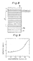
- the dielectric mirror layer 74 has a multiple layer structure including layers l1 and layers l2 which are alternatively layered as shown in Fig.8.
- the layer l1 is made of hydrogenated amorphous silicon carbide (a-Si 1-x C x :H).
- the layer l2 is also made of hydrogenated amorphous silicon carbide (a-Si 1-z C z :H) with different composition (Z ⁇ X).
- the dielectric mirror layer 74 consists of seventeen layers l1 and l2 and has a total layer thickness of about 1.3 ⁇ m.
- the dielectric mirror layer 74 thus constructed has a good reflecting capability and increases the resolution in image of the display device 70.
- the dielectric mirror layer 74 thus constructed has an advantage in its simplified manufacturing process, since both of the layers l1 and l2 are made of same material, i.e. hydrogenated amorphous silicon carbide.
- orientation films 75a and 75b are disposed on the transparent electrode 72a and the dielectric mirror layer 74.
- the substrates 71a and 71b are attached together by a sealing member 76.
- the liquid crystal layer 77 is disposed between the orientation films 75a and 75b.
- the display device 70 is operated in a same manner as the display device 10 of Fig. 1, by use of the laser beam L, the reading light R1 and the reflected light R2. Thus, the explanation for the operation of the display device 70 is omitted.
- a manufacturing procedure of the display device 70 will be explained below in sequence.
- the composition of the hydrogenated amorphous silicon carbide forming the dielectric mirror layer 73 is controlled by changing the gas flow volume ratio CH4/(SiH4 +CH4) of those material gases. Consequently, bewteen the forming process of the layer l1 and the forming process of the layer l2, there is no need changing the material gases but only changing the gas flow volume ratio of the material gases so as to obtain the layers l1 and l2 having desired compositions.
- the forming process of the dielectric mirror layer 74 in the present embodement is quite simplified compared with the case of forming the dielectric mirror layer having layers made of different material gases.
- the material gases for each layer forming process it is required to change the material gases for each layer forming process.
- a material gas of carbon for forming the hydrogenated amorphous silicon carbide layer as the dielectric mirror layer 74 ethane, propane, butane, acetylene and so on, can be used other than the methane.
- the sputtering method As a method of forming each layer l1 and l2 of the dielectric mirror layer 74, the sputtering method, the heat CVD method, the light CVD method, ECR plasma method etc., can be utilized other than the plasma CVD.
- the dielectric mirror layer 74 may be formed to include other materials such as oxigen and nitrogen.
- the molar composition Y of the silicon in the hydrogenated amorphous silicon carbide (a-Si y C 1-y :H) can be selected within a range of 0.1 to 0.9 and the molar composition X of the carbon in the hydrogenated amorphous silicon carbide (a-Si 1-x C x :H) can be selected within a range of 0.1 to 0.9 so that the refractive index n of the dielectric mirror layer 74 can be desirably selected.
- the molar composition Y is within a range of 0.1 to 0.5 and in a range of 0.7 to 0.9, while the molar composition X is within a range of 0.1 to 0.3 and 0.5 to 0.9.
- the number of layers l1 and l2 of the dielecric mirror layer 74 is not limited to seventeen, but it is preferably not less than ten, and more preferably not less than fifteen.
- Fig.10 shows a liquid crystal display apparatus, as a sixth embodiment of the present invention, utilizing three light valves each of which is same as the above described display device 70 of the fifth embodiment.
- the liquid crystal display apparatus 80 of color projection type is provided with three light valves 81a, 81b and 81c, each of which is same as the display device 70 of Fig.7.
- the light valves 81a, 81b and 81c are for R (red color), G (green color) and B (blue color) respectively.
- the light from the light source 85 is splitted into three colors of R,G,B by the prism 83 and the dichroic mirrors 82a, 82b and 82c. Then, the splitted lights are transmitted through the light valves 81a,81b,81c respectively, and combined together again by the prism 83. The combined light is then projected onto the screen 86 through the lens 84.
- Each of the light valves 81a,81b,81c is manufactured in the manner same as the display device 70 as described before, but the reflection coefficient charactristics on the wave length spectrum of the dielectric mirror layer in each light valve 81a,81b,81c is made different from each other so as to have its spectrum same as each corresponding R,G,B spectrum of the light source 85 respectively.
- the spectrum range, to which the dielectric mirror layer in each light valve 81a,81b,81c. is required to exhibit a high reflection coefficient is made narrow. This leads to reduce the thickness of the dielectric mirror layer.
- the thickness of the dielectric mirror layer is required to be thick about 1.3 ⁇ m as in the case mentioned in the display device 70.
- the thickness of the dielectric layer can be reduced to about 0.5 ⁇ m to 0.8 ⁇ m.
- the display apparatus 80 can be constructed with the light valves 81a,81b,81c suitable for color projection.
- Fig.11 shows a display device of a seventh embodiment according to the present invention.
- the same elements as those in Fig.7 carry the same reference numerals and the explanations thereof are omitted.
- a liquid crystal display device 90 of light scattering mode as its display mode is provided with a liquid crystal composite film 95b. Instead, the display device 90 is not provided with the orientation films which are provided in the display device 70.
- the manufacturing procedure of the display device 90 is same as that of the display device 70 to its step (D).
- the seventh embodiment after forming the dielectric mirror layer 74, the following process is performed to form the composite film 95b.
- a homogeneous solution in which about 30 weight % of a bifunctional acrylate (made by Nippon Kayaku Co., Ltd.) which is a UV polymarization compound, about 70 weight % of a nematic liquid crystal (ZLI 3201 000′ made by Merck Co., Inc.), and a small amount of polymarization initiator (Darocure 1173′ made by Merck Co., Inc.) are mixed together, is prepared and then filtered. Next, this prepared solution is spinner-coated on the dielectric mirror layer by about 10 ⁇ m. The coated film is then exposured by an ultraviolet ray to obtain the composite film 95b.
- a bifunctional acrylate made by Nippon Kayaku Co., Ltd.
- ZLI 3201 000′ made by Merck Co., Inc.
- a small amount of polymarization initiator Darocure 1173′ made by Merck Co., Inc.
- the glass substrate 71a, on which the transparent electrode 72a is formed, and the glass substrate 71b, on which the transparent electrode 72b, the photoconductive layer 73, the light absorbing layer 78, the dielectric mirror layer 74 and the composite film 95b are formed, are attached together by use of the sealing member 76 and the liquid crystal layer 77 is formed therebetween.
- an alternating electrical voltage is applied across the transparent electrodes 72a and 72b.
- a laser beam L scans the substrate 71b so as to change the impedance of the photoconductive layer 73, change the voltage applied to the liquid crystal layer 77, and change each molecular orientation in the voltage applied area of the liquid crystal layer 77 to a specific direction so as to transmit a reading light R1 therethrough.
- the molecular orientation directions are at randum so as to scatter the light R1 without transmitting the light R1.
- the light R1 transmitted through the liquid crystal layer 77 is reflected by the dielectric mirror layer 74 as a reflected reading light R2.
- the light R2 is then outputted from the display device 10 to be projected onto a screen.
- the seventh embodiment can be operated in the dynamic scattering mode.
- the nematic liquid crystal is used as the liquid crystal, however this is not mandatory. Instead, the present embodiment can utilize smetic liquid crystal or ferroelectric liquid crystal.
- a field induced birefringence mode the dynamic scattering mode, the HFE mode, the GH mode, the phase transition mode, and the TN mode can be utilized as the display mode.
- the birefringence mode, the GH mode and the light scattering mode can be utilized as the display mode.
Landscapes
- Physics & Mathematics (AREA)
- Nonlinear Science (AREA)
- Mathematical Physics (AREA)
- Chemical & Material Sciences (AREA)
- Crystallography & Structural Chemistry (AREA)
- General Physics & Mathematics (AREA)
- Optics & Photonics (AREA)
- Liquid Crystal (AREA)
Applications Claiming Priority (6)
| Application Number | Priority Date | Filing Date | Title |
|---|---|---|---|
| JP1208514A JP2761253B2 (ja) | 1989-08-11 | 1989-08-11 | 光書込み形液晶表示装置 |
| JP208514/89 | 1989-08-11 | ||
| JP257267/89 | 1989-10-02 | ||
| JP25726789 | 1989-10-02 | ||
| JP149273/90 | 1990-06-07 | ||
| JP2149273A JPH07104523B2 (ja) | 1989-10-02 | 1990-06-07 | 光書き込み型液晶表示素子 |
Publications (3)
| Publication Number | Publication Date |
|---|---|
| EP0412843A2 true EP0412843A2 (fr) | 1991-02-13 |
| EP0412843A3 EP0412843A3 (en) | 1992-05-06 |
| EP0412843B1 EP0412843B1 (fr) | 1996-05-29 |
Family
ID=27319715
Family Applications (1)
| Application Number | Title | Priority Date | Filing Date |
|---|---|---|---|
| EP90308843A Expired - Lifetime EP0412843B1 (fr) | 1989-08-11 | 1990-08-10 | Dispositif d'affichage à cristal liquide adressé optiquement |
Country Status (3)
| Country | Link |
|---|---|
| US (1) | US5245453A (fr) |
| EP (1) | EP0412843B1 (fr) |
| DE (1) | DE69027158T2 (fr) |
Cited By (4)
| Publication number | Priority date | Publication date | Assignee | Title |
|---|---|---|---|---|
| EP0547581A1 (fr) * | 1991-12-18 | 1993-06-23 | Sharp Kabushiki Kaisha | Procédé de fabrication d'une valve de lumière à crisal liquide couplée à un photoconducteur |
| EP0556985A1 (fr) * | 1992-02-04 | 1993-08-25 | Ngk Insulators, Ltd. | Modulateur spatial de lumière et sa méthode de fabrication |
| GB2373340A (en) * | 2001-03-13 | 2002-09-18 | Secr Defence | Optically addressed spatial light modulator |
| US7092046B2 (en) | 2001-03-13 | 2006-08-15 | Qinetiq Limited | Optically addressed spatial light modulator (OASLM) with dielectric mirror comprising layers of amorphous hydrogenated carbon |
Families Citing this family (12)
| Publication number | Priority date | Publication date | Assignee | Title |
|---|---|---|---|---|
| JP3102995B2 (ja) * | 1994-08-31 | 2000-10-23 | シャープ株式会社 | 液晶ライトバルブ |
| US20020184970A1 (en) | 2001-12-13 | 2002-12-12 | Wickersham Charles E. | Sptutter targets and methods of manufacturing same to reduce particulate emission during sputtering |
| JP4981233B2 (ja) | 2000-05-11 | 2012-07-18 | トーソー エスエムディー,インク. | 音波の位相変化の検出を使用する、スパッターターゲット清浄度の非破壊評価のための方法と装置 |
| WO2002081767A2 (fr) | 2001-04-04 | 2002-10-17 | Tosoh Smd, Inc. | Procede permettant de determiner une dimension critique d'une inclusion d'oxyde d'aluminium dans une cible de pulverisation cathodique en aluminium ou en alliage d'aluminium |
| US6903512B2 (en) * | 2001-08-07 | 2005-06-07 | Konica Corporation | Half mirror film producing method and optical element comprising a half mirror film |
| JP4349904B2 (ja) | 2001-08-09 | 2009-10-21 | トーソー エスエムディー,インク. | 寸法と位置によって分類された欠陥の種類による、非破壊的なターゲット清浄度特性決定のための方法と装置 |
| JP3937807B2 (ja) | 2001-11-01 | 2007-06-27 | 富士ゼロックス株式会社 | 光アドレス型空間光変調素子 |
| JP4004908B2 (ja) * | 2002-09-26 | 2007-11-07 | 富士通株式会社 | 表示装置の駆動方法及び装置 |
| KR20050001425A (ko) * | 2003-06-27 | 2005-01-06 | 아사히 가라스 가부시키가이샤 | 고반사경 |
| WO2012037445A2 (fr) | 2010-09-17 | 2012-03-22 | Drexel University | Nouvelles applications pour carbone alliforme |
| US9752932B2 (en) | 2010-03-10 | 2017-09-05 | Drexel University | Tunable electro-optic filter stack |
| KR102456533B1 (ko) | 2017-05-23 | 2022-10-19 | 삼성전자주식회사 | 홀로그램 재생 장치 및 그 제어 방법 |
Citations (1)
| Publication number | Priority date | Publication date | Assignee | Title |
|---|---|---|---|---|
| US4019807A (en) * | 1976-03-08 | 1977-04-26 | Hughes Aircraft Company | Reflective liquid crystal light valve with hybrid field effect mode |
Family Cites Families (14)
| Publication number | Priority date | Publication date | Assignee | Title |
|---|---|---|---|---|
| AU4208972A (en) * | 1971-05-15 | 1973-11-15 | Amalgamated Wireless (Australasia) Limited | Improvements in or relating to electro-optical display devices |
| US4538884A (en) * | 1981-07-10 | 1985-09-03 | Canon Kabushiki Kaisha | Electro-optical device and method of operating same |
| JPS5981627A (ja) * | 1982-11-01 | 1984-05-11 | Nec Corp | 光書込型液晶ライトバルブ素子 |
| JPS60119567A (ja) * | 1983-12-01 | 1985-06-27 | Ricoh Co Ltd | 電子写真感光体 |
| JPS62172758A (ja) * | 1986-01-27 | 1987-07-29 | Fujitsu Ltd | 薄膜トランジスタの構造 |
| JPS63253924A (ja) * | 1987-04-10 | 1988-10-20 | Seiko Epson Corp | ライトバルブ及びその製造法 |
| US4762397A (en) * | 1987-06-19 | 1988-08-09 | Hughes Aircraft Company | Optical phase conjugator with spatially resolvable thresholding utilizing liquid crystal light valve |
| EP0359801B1 (fr) * | 1987-12-30 | 1995-05-17 | Hughes Aircraft Company | Materiau a cristaux liquides disperses dans un polymere d'acrylate et dispositifs realises a partir de ce materiau |
| JPH0283524A (ja) * | 1988-09-20 | 1990-03-23 | Dainippon Ink & Chem Inc | 液晶デバイス及びその製造方法 |
| US4941735A (en) * | 1989-03-02 | 1990-07-17 | University Of Colorado Foundation, Inc. | Optically addressable spatial light modulator |
| JP2724207B2 (ja) * | 1989-06-01 | 1998-03-09 | シャープ株式会社 | 強誘電性液晶素子及び光書込み型液晶表示装置 |
| US5084777A (en) * | 1989-11-14 | 1992-01-28 | Greyhawk Systems, Inc. | Light addressed liquid crystal light valve incorporating electrically insulating light blocking material of a-SiGe:H |
| US5132814A (en) * | 1990-01-26 | 1992-07-21 | Victor Company Of Japan, Ltd. | Liquid crystal spatial light modulator with multilayer photoconductor |
| EP0468529B1 (fr) * | 1990-07-26 | 1995-01-25 | Asahi Glass Company Ltd. | Elément d'affichage à cristal liquide à matrice active et dispositif de projection à afficheur à cristal liquide à matrice active |
-
1990
- 1990-08-10 DE DE69027158T patent/DE69027158T2/de not_active Expired - Fee Related
- 1990-08-10 EP EP90308843A patent/EP0412843B1/fr not_active Expired - Lifetime
-
1992
- 1992-06-19 US US07/902,417 patent/US5245453A/en not_active Expired - Lifetime
Patent Citations (1)
| Publication number | Priority date | Publication date | Assignee | Title |
|---|---|---|---|---|
| US4019807A (en) * | 1976-03-08 | 1977-04-26 | Hughes Aircraft Company | Reflective liquid crystal light valve with hybrid field effect mode |
Non-Patent Citations (3)
| Title |
|---|
| APPLIED PHYSICS LETTERS, vol. 51, no. 16, 19th October 1987, pages 1233-1235, Ammerican Institute of Physics, New York, NY, US; N. SHIN-ICHI TAKAHASHI et al.: "High-speed light valve using an amorphous silicon photosensor and ferroelectric liquid crystals" * |
| APPLIED PHYSICS LETTERS, vol. 55, no. 6, 7th August 1989, pages 537-539, American Institute of Physics; G. MODDEL et al.: "High-speed binary optically addressed spatial light modulator" * |
| J. SCHLICHTING et al.: "GMELIN HANDBOOK OF INORGANIC CHEMISTRY", supplement vol. B2, system no. 15, 1984, 8th edition, editors G. Kirschstein et al., pages 283-307, Springer-Verlag, Berlin, DE; * |
Cited By (9)
| Publication number | Priority date | Publication date | Assignee | Title |
|---|---|---|---|---|
| EP0547581A1 (fr) * | 1991-12-18 | 1993-06-23 | Sharp Kabushiki Kaisha | Procédé de fabrication d'une valve de lumière à crisal liquide couplée à un photoconducteur |
| US5324549A (en) * | 1991-12-18 | 1994-06-28 | Sharp Kabushiki Kaisha | Method of fabricating photoconductor coupled liquid crystal light valve |
| EP0556985A1 (fr) * | 1992-02-04 | 1993-08-25 | Ngk Insulators, Ltd. | Modulateur spatial de lumière et sa méthode de fabrication |
| US5471331A (en) * | 1992-02-04 | 1995-11-28 | Nippon Hoso Kyokai | Spatial light modulator element with amorphous film of germanium, carbon and silicon for light blocking layer |
| EP0722112A2 (fr) * | 1992-02-04 | 1996-07-17 | Ngk Insulators, Ltd. | Modulateur spatial de lumière et sa méthode de fabrication |
| EP0722112A3 (fr) * | 1992-02-04 | 1996-07-31 | Ngk Insulators Ltd | |
| GB2373340A (en) * | 2001-03-13 | 2002-09-18 | Secr Defence | Optically addressed spatial light modulator |
| US7092046B2 (en) | 2001-03-13 | 2006-08-15 | Qinetiq Limited | Optically addressed spatial light modulator (OASLM) with dielectric mirror comprising layers of amorphous hydrogenated carbon |
| USRE43642E1 (en) | 2001-03-13 | 2012-09-11 | F. Poszat Hu, Llc | Optically addressed spatial light modulator (OASLM) with dielectric mirror comprising layers of amorphous hydrogenated carbon |
Also Published As
| Publication number | Publication date |
|---|---|
| EP0412843A3 (en) | 1992-05-06 |
| EP0412843B1 (fr) | 1996-05-29 |
| DE69027158T2 (de) | 1996-10-24 |
| DE69027158D1 (de) | 1996-07-04 |
| US5245453A (en) | 1993-09-14 |
Similar Documents
| Publication | Publication Date | Title |
|---|---|---|
| EP0412843A2 (fr) | Dispositif d'affichage à cristal liquide adressé optiquement | |
| US5329390A (en) | Liquid crystal display element of optical writing type with light absorbing layer including inorganic pigment and leveling layer | |
| US5640260A (en) | Liquid crystal light valve having a Eopt of less than 0.5 eV | |
| US5142391A (en) | Liquid-crystal display device of optical writing type having a light absorbing layer composed of a carbon-dispersed system coating | |
| US5305129A (en) | Liquid crystal display device of optical writing type having a carbon dispersed light absorbing layer and a cholesteric reflector | |
| EP0556985B1 (fr) | Modulateur spatial de lumière et sa méthode de fabrication | |
| JPH10239669A (ja) | 反射型液晶表示装置 | |
| US7092046B2 (en) | Optically addressed spatial light modulator (OASLM) with dielectric mirror comprising layers of amorphous hydrogenated carbon | |
| US5315420A (en) | Optical writing type liquid crystal display device | |
| Takizawa et al. | Spatial light modulators for projection displays | |
| USRE43642E1 (en) | Optically addressed spatial light modulator (OASLM) with dielectric mirror comprising layers of amorphous hydrogenated carbon | |
| JPH0367247B2 (fr) | ||
| US5268779A (en) | Spatial light modulator with composite film formed by vapor deposition of light blocking semiconductor material and insulation material | |
| JP2816686B2 (ja) | 液晶装置 | |
| JPH07134310A (ja) | 光書き込み型電気光学装置 | |
| JPH07104523B2 (ja) | 光書き込み型液晶表示素子 | |
| JP3073657B2 (ja) | 液晶ライトバルブ及びそれを用いた投射型液晶表示装置 | |
| JPH0792487A (ja) | 光変調素子 | |
| JPH0933942A (ja) | 空間光変調素子およびその製造方法 | |
| JP2567820B2 (ja) | 液晶表示装置 | |
| JP2769395B2 (ja) | 液晶ライトバルブ | |
| JPH0829800A (ja) | 光書き込み型液晶ライトバルブ | |
| JPH05273527A (ja) | 液晶表示素子 | |
| JPH06283731A (ja) | 空間光変調素子の製造方法 | |
| JPH10170948A (ja) | 空間光変調素子及びその製造方法 |
Legal Events
| Date | Code | Title | Description |
|---|---|---|---|
| PUAI | Public reference made under article 153(3) epc to a published international application that has entered the european phase |
Free format text: ORIGINAL CODE: 0009012 |
|
| AK | Designated contracting states |
Kind code of ref document: A2 Designated state(s): DE FR GB NL |
|
| 17P | Request for examination filed |
Effective date: 19901220 |
|
| RIN1 | Information on inventor provided before grant (corrected) |
Inventor name: FUJIWARA, SAYURI Inventor name: KIMURA, NAOFUMI Inventor name: HATANO, AKITSUGU |
|
| PUAL | Search report despatched |
Free format text: ORIGINAL CODE: 0009013 |
|
| AK | Designated contracting states |
Kind code of ref document: A3 Designated state(s): DE FR GB NL |
|
| 17Q | First examination report despatched |
Effective date: 19940624 |
|
| GRAH | Despatch of communication of intention to grant a patent |
Free format text: ORIGINAL CODE: EPIDOS IGRA |
|
| GRAA | (expected) grant |
Free format text: ORIGINAL CODE: 0009210 |
|
| AK | Designated contracting states |
Kind code of ref document: B1 Designated state(s): DE FR GB NL |
|
| REF | Corresponds to: |
Ref document number: 69027158 Country of ref document: DE Date of ref document: 19960704 |
|
| ET | Fr: translation filed | ||
| PLBE | No opposition filed within time limit |
Free format text: ORIGINAL CODE: 0009261 |
|
| STAA | Information on the status of an ep patent application or granted ep patent |
Free format text: STATUS: NO OPPOSITION FILED WITHIN TIME LIMIT |
|
| 26N | No opposition filed | ||
| PGFP | Annual fee paid to national office [announced via postgrant information from national office to epo] |
Ref country code: DE Payment date: 20010806 Year of fee payment: 12 |
|
| PGFP | Annual fee paid to national office [announced via postgrant information from national office to epo] |
Ref country code: GB Payment date: 20010808 Year of fee payment: 12 |
|
| PGFP | Annual fee paid to national office [announced via postgrant information from national office to epo] |
Ref country code: FR Payment date: 20010810 Year of fee payment: 12 |
|
| PGFP | Annual fee paid to national office [announced via postgrant information from national office to epo] |
Ref country code: NL Payment date: 20010830 Year of fee payment: 12 |
|
| REG | Reference to a national code |
Ref country code: GB Ref legal event code: IF02 |
|
| PG25 | Lapsed in a contracting state [announced via postgrant information from national office to epo] |
Ref country code: GB Free format text: LAPSE BECAUSE OF NON-PAYMENT OF DUE FEES Effective date: 20020810 |
|
| PG25 | Lapsed in a contracting state [announced via postgrant information from national office to epo] |
Ref country code: NL Free format text: LAPSE BECAUSE OF NON-PAYMENT OF DUE FEES Effective date: 20030301 Ref country code: DE Free format text: LAPSE BECAUSE OF NON-PAYMENT OF DUE FEES Effective date: 20030301 |
|
| GBPC | Gb: european patent ceased through non-payment of renewal fee |
Effective date: 20020810 |
|
| PG25 | Lapsed in a contracting state [announced via postgrant information from national office to epo] |
Ref country code: FR Free format text: LAPSE BECAUSE OF NON-PAYMENT OF DUE FEES Effective date: 20030430 |
|
| NLV4 | Nl: lapsed or anulled due to non-payment of the annual fee |
Effective date: 20030301 |
|
| REG | Reference to a national code |
Ref country code: FR Ref legal event code: ST |