EP0407933A2 - Dispositif semi-conducteur scellé par une résine dont la résistance aux contraintes thermiques est améliorée - Google Patents
Dispositif semi-conducteur scellé par une résine dont la résistance aux contraintes thermiques est améliorée Download PDFInfo
- Publication number
- EP0407933A2 EP0407933A2 EP90113061A EP90113061A EP0407933A2 EP 0407933 A2 EP0407933 A2 EP 0407933A2 EP 90113061 A EP90113061 A EP 90113061A EP 90113061 A EP90113061 A EP 90113061A EP 0407933 A2 EP0407933 A2 EP 0407933A2
- Authority
- EP
- European Patent Office
- Prior art keywords
- wiring
- semiconductor device
- wiring layer
- dummy
- wirings
- Prior art date
- Legal status (The legal status is an assumption and is not a legal conclusion. Google has not performed a legal analysis and makes no representation as to the accuracy of the status listed.)
- Withdrawn
Links
Images
Classifications
-
- H—ELECTRICITY
- H10—SEMICONDUCTOR DEVICES; ELECTRIC SOLID-STATE DEVICES NOT OTHERWISE PROVIDED FOR
- H10W—GENERIC PACKAGES, INTERCONNECTIONS, CONNECTORS OR OTHER CONSTRUCTIONAL DETAILS OF DEVICES COVERED BY CLASS H10
- H10W20/00—Interconnections in chips, wafers or substrates
- H10W20/40—Interconnections external to wafers or substrates, e.g. back-end-of-line [BEOL] metallisations or vias connecting to gate electrodes
- H10W20/41—Interconnections external to wafers or substrates, e.g. back-end-of-line [BEOL] metallisations or vias connecting to gate electrodes characterised by their conductive parts
- H10W20/42—Vias, e.g. via plugs
-
- H—ELECTRICITY
- H10—SEMICONDUCTOR DEVICES; ELECTRIC SOLID-STATE DEVICES NOT OTHERWISE PROVIDED FOR
- H10W—GENERIC PACKAGES, INTERCONNECTIONS, CONNECTORS OR OTHER CONSTRUCTIONAL DETAILS OF DEVICES COVERED BY CLASS H10
- H10W72/00—Interconnections or connectors in packages
- H10W72/50—Bond wires
- H10W72/531—Shapes of wire connectors
- H10W72/536—Shapes of wire connectors the connected ends being ball-shaped
-
- H—ELECTRICITY
- H10—SEMICONDUCTOR DEVICES; ELECTRIC SOLID-STATE DEVICES NOT OTHERWISE PROVIDED FOR
- H10W—GENERIC PACKAGES, INTERCONNECTIONS, CONNECTORS OR OTHER CONSTRUCTIONAL DETAILS OF DEVICES COVERED BY CLASS H10
- H10W72/00—Interconnections or connectors in packages
- H10W72/50—Bond wires
- H10W72/59—Bond pads specially adapted therefor
-
- H—ELECTRICITY
- H10—SEMICONDUCTOR DEVICES; ELECTRIC SOLID-STATE DEVICES NOT OTHERWISE PROVIDED FOR
- H10W—GENERIC PACKAGES, INTERCONNECTIONS, CONNECTORS OR OTHER CONSTRUCTIONAL DETAILS OF DEVICES COVERED BY CLASS H10
- H10W72/00—Interconnections or connectors in packages
- H10W72/90—Bond pads, in general
- H10W72/951—Materials of bond pads
- H10W72/952—Materials of bond pads comprising metals or metalloids, e.g. PbSn, Ag or Cu
-
- H—ELECTRICITY
- H10—SEMICONDUCTOR DEVICES; ELECTRIC SOLID-STATE DEVICES NOT OTHERWISE PROVIDED FOR
- H10W—GENERIC PACKAGES, INTERCONNECTIONS, CONNECTORS OR OTHER CONSTRUCTIONAL DETAILS OF DEVICES COVERED BY CLASS H10
- H10W72/00—Interconnections or connectors in packages
- H10W72/90—Bond pads, in general
- H10W72/981—Auxiliary members, e.g. spacers
- H10W72/983—Reinforcing structures, e.g. collars
Definitions
- the present invention relates to a semiconductor device, and more particularly to a resin sealed semiconductor device.
- a resin sealed semiconductor device is ordinarily assembled by mounting on a lead frame a semiconductor element which has circuit elements formed thereon, connecting the electrodes of the semiconductor element and the leads of the lead frame with bonding wires and sealing the semiconductor element and wires with a resin member.
- a resin sealed semiconductor device is constructed having components that may be roughly divided into an epoxy resin member which is a sealing material, a silicon substrate with circuit elements formed thereon and a metallic lead frame on which is mounted a silicon substrate. Since the coefficients of thremal expansion of these materials are mutually different, thermal stresses are generated at the respective boundaries of the epoxy resin member, the silicon substrate and the lead frame due to expansion or contraction that occurs due to changes in the temperature.
- a bonding ball is formed at a part of the wire that is connected to a bonding pad on the silicon substrate.
- the bonding ball is given a shape that protrudes from the upper surface of the silicon substrate so that it is subjected most severely to the influence of the stresses in the epoxy resin when a temperature change takes place.
- the bonding pad which is connected to the bonding ball suffers from large stresses.
- the component of the stresses that acts in the direction parallel to the substrate surface, which generates a shear in the bonding pad and creates a change in its shape. The deformation thus created is spread to the circuit element of the output buffer circuit via a leader line which is connected to the bonding pad.
- the tip of the leader line is connected via contacts to a diffused layer on the silicon substratel the spreading deformation in the leader line acts on the contacts as a concentration of stresses.
- the contacts can no longer withstand the stress concentration, the lead line is broken. Further, the stress concentration cause pressure on the wirings which are on a level lower than that of the lead line, thus causing disconnections of the lower level wirings.
- the conventional countermeasures to the above mentioned problems are as follows. Firstly, a resin with a coefficient of expansion made to match that of silicon is employed. This is obtained by blending various kinds of fillers with a resin, such as epoxy resin, which has a coefficient of thermal expansion close to that of silicon. Secondly, the width of the wirings in the portion receiving large stresses is increased, or the spacing between the wirings is increased.
- the sealing resin having a coefficient of expansion made to match that of silicon has an inferior moisture resistance creating a separate problem that the moisture resistance of the semiconductor device is deteriorated.
- the effort to improve the integration density of the semiconductor device is obstructed, its electrical capacitance increased, and the operating speed is reduced.
- At least a part, for example, a leader line, of the wirings on the uppermost level provided on the silicon substrate is connected to a lower level dummy wiring.
- the dummy wiring is not connected to other parts of the semiconductor device via a through hole formed on the part of an interlayer film directly beneath that part of the wiring under discussion as in the convertional structure.
- the lower level dummy wiring plays the role of a stopper for stopping the etching of the through hole, at the time of through hole formation, and; it can be formed at the same time as the formation of other wirings required for the construction of the circuit, so that there is no need for any special fabrication process for the provision of the dummy wiring.
- the dummy wiring and the through hole act to hold back the leader line which tends to slip in the layer direction when a shear stress acts on the lead line due to the changes in the temperature.
- the dummy wiring and the through hole play the role of an anchor.
- the same materials as in the prior art can be used for the fabrication of a semiconductor device, and moreover, it is possible to avoid the breaking of the wirings by providing a strength that can withstand thermal stresses when the device is subjected to the thermal stresses.
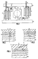
- a resin sealed semiconductor device in accordance with the first embodiment of the present invention comprises a bonding pad 1 which is an uppermost level wiring layer, a circuit element (a group of MOS transistors) 2 which constitutes an output buffer circuit, a leader line 3 which is an upper level wiring layer that connects the bonding pad 1 and the circuit element 2, a power supply wiring 4a and a ground wiring 4b which are also uppermost level wiring layers, an input wiring 5 to the circuit element 2 and an independent, islandlike dummy wiring 7 which are lower level wiring layers that are provided beneath the uppermost level wirings via an insulating layer (12 of Figs. 2 to 4), and a contact 6 provided in a diffused layer in the surface of the silicon substrate for connection to the uppermost level wiring layer.
- a bonding pad 1 which is an uppermost level wiring layer
- a circuit element (a group of MOS transistors) 2 which constitutes an output buffer circuit
- a leader line 3 which is an upper level wiring layer that connects the bonding pad 1 and the circuit element 2
- a semiconductor element formed as in the above is mounted on a lead frame (not shown), bonding wires (not shown) are connected to the bonding pad 1, and then the device is resin sealed.
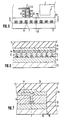
- a 0.5 ⁇ m-thick first interlayer film 11 that uses phosphosilicate glass is formed on the silicon substrate with circuit elements 2 formed thereon.
- input wirings 5 see Fig. 1
- dummy wirings 7 see Figs. 1 to 3 are formed to a thickness of 0.4 ⁇ m using polycrystalline silicon on the first interlayer film 11.
- the dummy wiring 7 is formed at a position directly beneath the lead line 3, but it is not connected to other lower level wiring layers.
- the dummy wiring 7 is an independent and islandiike metallic layer, with dimensions of 10 ⁇ m x 10 ⁇ m.
- a second interlayer film 12 is formed to a thickness of 1 ⁇ m so as to cover the lower level wiring layers 5 and 7 and the first interlayer film 11.
- a through hole 8 with length and width respectively in the range of 1.5 to 2.0 ⁇ m is created by etching in the second interlayer film 12 formed on the dummy wiring 7.
- the dummy wiring 7 plays the role of a stopper which stops the etching of the through hole 8.
- the material for the second interlayer film 12 is the same as the material for the first interlayer film 11.
- the lead lines 3, the bonding pad 1, the power supply wiring 4a and the ground wiring 4b are formed of aluminum to a thickness of 1 ⁇ m as the upper level wiring layers, on the through holes 8.
- each of the through holes 8 is simultaneously filled with aluminum so that the dummy wiring 7 and the lead line 3 are firmly bonded via the through hole 8.
- the width of the lead line 3 is set to 10 ⁇ m, and the dimensions of the bonding pad are set to 100 ⁇ m x 100 ⁇ m.
- the peripheral part of the bonding pad 1, the entirety of other upper level wiring layers 3, 4a and 4b and the second interlayer film 12 are coated with a passivation film 13 of silicon nitride or phosphosilicate glass. It should be noted that the presence of the passivation film 13 is not indicated in Fig. 1.
- a semiconductor element formed as in the above is mounted on a lead frame (not shown), connected to external terminals, namely, leads (not shown) of the lead frame via the bonding ball 9, and is sealed with a resin number 14 (not indicated in Fig. 1) such as one of epoxy resin.
- the first embodiment there is formed a dummy wiring 7 and a through hole 8 for each leader line 3.
- a plurality of dummy wirings and through holes may be formed as needed.
- the dimensions of the dummy wiring suffices if they are at least larger than the dimensions of the through hole (for example, the dummy wiring may be a square with side larger than 3 ⁇ m).
- the sides of the square may be larger than 10 ⁇ m provided that the dummy wiring remains within a defined range and does not approach the lower level wirings in its surroundings.
- the shape of the dummy wiring need not be square, and may be rectangular or bent.
- the wiring 4c is formed so as to extend in the direction of the plurality of dummy wirings 7, where each dummy wiring 7 is connected to the outermost wiring 4c via a through hole 8.
- the wiring 4c which is arranged at the outermost part of the semiconductor chip is an important wiring ordinarily used as a power supply wire or a ground wiring.
- the outermost wiring 4c is subjected to large thermal stresses in the sealing resin 14 that are generated by the changes in the temperature.
- deformation of the outermost wiring 4c is suppressed by the large number of dummy wirings 7 and the through holes 8 arranged in the periphery of the semiconductor chip acting as anchors and protecting the contacts 6 that are linked to these wirings.
- a temperature cycling test is given to the semiconductor devices according to the two embodiments of the present invention described above. Namely, a semiconductor device with semiconductor chip area of 60 to 70 mm2 is subjected to 300 temperature cyclings in one hour during which the temperature of the device is raised from -60°C through room temperature to +150°C and then lowered back to -60°C in the reverse direction. A lot consisting of 20 to 50 pieces of the semiconductor devices is judged a defective lot if even one incidence of a disconnection defect is detected by the test.
- the semiconductor device of the present invention can be fabricated by the same process using the same materials as in the conventional semiconductor device, there is no need for modifying the coefficient of thermal expansion or changing the dimensions of the wiring on the semiconductor chip. As a result, it becomes possible to improve the yield strength to the temperature cycling without sacrificing the moisture resistance and the electrical characteristic of the semiconductor device.
Landscapes
- Internal Circuitry In Semiconductor Integrated Circuit Devices (AREA)
Applications Claiming Priority (2)
| Application Number | Priority Date | Filing Date | Title |
|---|---|---|---|
| JP17743989 | 1989-07-10 | ||
| JP177439/89 | 1989-07-10 |
Publications (2)
| Publication Number | Publication Date |
|---|---|
| EP0407933A2 true EP0407933A2 (fr) | 1991-01-16 |
| EP0407933A3 EP0407933A3 (en) | 1991-07-31 |
Family
ID=16030966
Family Applications (1)
| Application Number | Title | Priority Date | Filing Date |
|---|---|---|---|
| EP19900113061 Withdrawn EP0407933A3 (en) | 1989-07-10 | 1990-07-09 | Resin sealed semiconductor device with improved thermal stress resistance |
Country Status (3)
| Country | Link |
|---|---|
| US (1) | US5117280A (fr) |
| EP (1) | EP0407933A3 (fr) |
| JP (1) | JPH03129738A (fr) |
Cited By (4)
| Publication number | Priority date | Publication date | Assignee | Title |
|---|---|---|---|---|
| EP0538619A1 (fr) * | 1991-10-22 | 1993-04-28 | Mitsubishi Denki Kabushiki Kaisha | Conducteur multicouche pour dispositif semi-conducteur et son procédé de fabrication |
| US5391920A (en) * | 1991-07-09 | 1995-02-21 | Yamaha Corporation | Semiconductor device having peripheral metal wiring |
| EP0707341A1 (fr) * | 1994-10-06 | 1996-04-17 | Altera Corporation | Puce de circuit intégré comprenant des motifs métalliques placés aux coins |
| EP1030367A3 (fr) * | 1999-02-19 | 2003-05-02 | Infineon Technologies AG | Dispositif semi-conducteur avec des lignes conductrices stabilisées |
Families Citing this family (17)
| Publication number | Priority date | Publication date | Assignee | Title |
|---|---|---|---|---|
| US5280194A (en) * | 1988-11-21 | 1994-01-18 | Micro Technology Partners | Electrical apparatus with a metallic layer coupled to a lower region of a substrate and metallic layer coupled to a lower region of a semiconductor device |
| JP3238395B2 (ja) * | 1990-09-28 | 2001-12-10 | 株式会社東芝 | 半導体集積回路 |
| KR960007643B1 (en) * | 1991-02-07 | 1996-06-07 | Nippon Electric Co | Semiconductor device sealed by resin |
| JP2988075B2 (ja) * | 1991-10-19 | 1999-12-06 | 日本電気株式会社 | 半導体装置 |
| JPH06125013A (ja) * | 1992-03-14 | 1994-05-06 | Toshiba Corp | 半導体装置及びその製造方法 |
| US5403729A (en) * | 1992-05-27 | 1995-04-04 | Micro Technology Partners | Fabricating a semiconductor with an insulative coating |
| US5592022A (en) * | 1992-05-27 | 1997-01-07 | Chipscale, Inc. | Fabricating a semiconductor with an insulative coating |
| US5656547A (en) * | 1994-05-11 | 1997-08-12 | Chipscale, Inc. | Method for making a leadless surface mounted device with wrap-around flange interface contacts |
| GB2302452B (en) * | 1994-06-09 | 1998-11-18 | Chipscale Inc | Resistor fabrication |
| JP2940432B2 (ja) * | 1995-04-27 | 1999-08-25 | ヤマハ株式会社 | 半導体装置とその製造方法 |
| JP3548082B2 (ja) * | 2000-03-30 | 2004-07-28 | 三洋電機株式会社 | 半導体装置及びその製造方法 |
| JP2003045876A (ja) * | 2001-08-01 | 2003-02-14 | Seiko Epson Corp | 半導体装置 |
| US6833323B2 (en) * | 2003-01-29 | 2004-12-21 | Taiwan Semiconductor Manufacturing Co., Ltd | Method for forming patterned features at a semiconductor wafer periphery to prevent metal peeling |
| JP5552261B2 (ja) * | 2009-05-12 | 2014-07-16 | パナソニック株式会社 | 半導体装置 |
| ITUB20160251A1 (it) * | 2016-02-01 | 2017-08-01 | St Microelectronics Srl | Procedimento per ridurre gli stress termo-meccanici in dispositivi a semiconduttore e corrispondente dispositivo |
| US11469194B2 (en) | 2018-08-08 | 2022-10-11 | Stmicroelectronics S.R.L. | Method of manufacturing a redistribution layer, redistribution layer and integrated circuit including the redistribution layer |
| CN113066790B (zh) * | 2021-03-19 | 2026-01-27 | 日月光半导体制造股份有限公司 | 半导体封装装置及其制造方法 |
Family Cites Families (7)
| Publication number | Priority date | Publication date | Assignee | Title |
|---|---|---|---|---|
| JPS6010645A (ja) * | 1983-06-30 | 1985-01-19 | Toshiba Corp | 樹脂封止型半導体装置 |
| JPS60138940A (ja) * | 1983-12-27 | 1985-07-23 | Toshiba Corp | 半導体装置の製造方法 |
| JPS6153745A (ja) * | 1984-08-24 | 1986-03-17 | Fujitsu Ltd | アルミニウム多層配線 |
| JPS61194747A (ja) * | 1985-02-22 | 1986-08-29 | Mitsubishi Electric Corp | 樹脂封止型半導体集積回路装置 |
| US4884123A (en) * | 1987-02-19 | 1989-11-28 | Advanced Micro Devices, Inc. | Contact plug and interconnect employing a barrier lining and a backfilled conductor material |
| JPS6450443A (en) * | 1987-08-20 | 1989-02-27 | Toshiba Corp | Semiconductor device |
| JPH01302842A (ja) * | 1988-05-31 | 1989-12-06 | Nec Corp | 多層配線構造の半導体装置 |
-
1990
- 1990-07-05 JP JP2178132A patent/JPH03129738A/ja active Pending
- 1990-07-09 EP EP19900113061 patent/EP0407933A3/en not_active Withdrawn
- 1990-07-10 US US07/550,848 patent/US5117280A/en not_active Expired - Lifetime
Cited By (7)
| Publication number | Priority date | Publication date | Assignee | Title |
|---|---|---|---|---|
| US5391920A (en) * | 1991-07-09 | 1995-02-21 | Yamaha Corporation | Semiconductor device having peripheral metal wiring |
| US5491352A (en) * | 1991-07-09 | 1996-02-13 | Yamaha Corporation | Semiconductor device having peripheral metal wiring |
| EP0538619A1 (fr) * | 1991-10-22 | 1993-04-28 | Mitsubishi Denki Kabushiki Kaisha | Conducteur multicouche pour dispositif semi-conducteur et son procédé de fabrication |
| US5444186A (en) * | 1991-10-22 | 1995-08-22 | Mitsubishi Denki Kabushiki Kaisha | Multilayer conductive wire for semiconductor device and manufacturing method thereof |
| EP0707341A1 (fr) * | 1994-10-06 | 1996-04-17 | Altera Corporation | Puce de circuit intégré comprenant des motifs métalliques placés aux coins |
| US5572067A (en) * | 1994-10-06 | 1996-11-05 | Altera Corporation | Sacrificial corner structures |
| EP1030367A3 (fr) * | 1999-02-19 | 2003-05-02 | Infineon Technologies AG | Dispositif semi-conducteur avec des lignes conductrices stabilisées |
Also Published As
| Publication number | Publication date |
|---|---|
| JPH03129738A (ja) | 1991-06-03 |
| EP0407933A3 (en) | 1991-07-31 |
| US5117280A (en) | 1992-05-26 |
Similar Documents
| Publication | Publication Date | Title |
|---|---|---|
| US5117280A (en) | Plastic package semiconductor device with thermal stress resistant structure | |
| US6759307B1 (en) | Method to prevent die attach adhesive contamination in stacked chips | |
| US20030000082A1 (en) | IC package with dual heat spreaders | |
| JP3999720B2 (ja) | 半導体装置およびその製造方法 | |
| WO1999019907A1 (fr) | Procede et construction renforçant thermiquement une enceinte micro-electronique | |
| JPH1056093A (ja) | 半導体装置およびその半導体装置を組み込んだ電子装置 | |
| JPH10335372A (ja) | 改良されたパッケージングのための集積回路チップ構造 | |
| US5349233A (en) | Lead frame and semiconductor module using the same having first and second islands and three distinct pluralities of leads and semiconductor module using the lead frame | |
| US5780923A (en) | Modified bus bar with Kapton™ tape or insulative material on LOC packaged part | |
| US11694950B2 (en) | Semiconductor package | |
| JPH0590452A (ja) | 樹脂封止型半導体装置 | |
| JPS61194747A (ja) | 樹脂封止型半導体集積回路装置 | |
| JPS6220707B2 (fr) | ||
| EP0405501B1 (fr) | Dispositif à semi-conducteurs | |
| KR100207902B1 (ko) | 리드 프레임을 이용한 멀티 칩 패키지 | |
| JP4498336B2 (ja) | 半導体装置および半導体装置の製造方法 | |
| JP3206035B2 (ja) | 樹脂封止型半導体装置 | |
| KR0138301B1 (ko) | 리드 온 칩(loc) 구조의 패키지 | |
| KR19980025889A (ko) | 중합체층이 개재된 반도체 칩과 기판 간의 범프 접속 구조 | |
| EP0646963A1 (fr) | Module à multi-puces et méthode de fabrication | |
| JPS6298633A (ja) | 半導体装置 | |
| JPH0511661B2 (fr) | ||
| JP2595874B2 (ja) | マルチチップモジュール | |
| JPS62193137A (ja) | 半導体装置の製造方法 | |
| JPS63143836A (ja) | 半導体装置 |
Legal Events
| Date | Code | Title | Description |
|---|---|---|---|
| PUAI | Public reference made under article 153(3) epc to a published international application that has entered the european phase |
Free format text: ORIGINAL CODE: 0009012 |
|
| 17P | Request for examination filed |
Effective date: 19900709 |
|
| AK | Designated contracting states |
Kind code of ref document: A2 Designated state(s): DE FR GB |
|
| PUAL | Search report despatched |
Free format text: ORIGINAL CODE: 0009013 |
|
| RHK1 | Main classification (correction) |
Ipc: H01L 23/522 |
|
| AK | Designated contracting states |
Kind code of ref document: A3 Designated state(s): DE FR GB |
|
| 17Q | First examination report despatched |
Effective date: 19940307 |
|
| STAA | Information on the status of an ep patent application or granted ep patent |
Free format text: STATUS: THE APPLICATION HAS BEEN WITHDRAWN |
|
| 18W | Application withdrawn |
Withdrawal date: 19970711 |