EP0401792A2 - Halbleiterspeicheranordnung - Google Patents
Halbleiterspeicheranordnung Download PDFInfo
- Publication number
- EP0401792A2 EP0401792A2 EP90110712A EP90110712A EP0401792A2 EP 0401792 A2 EP0401792 A2 EP 0401792A2 EP 90110712 A EP90110712 A EP 90110712A EP 90110712 A EP90110712 A EP 90110712A EP 0401792 A2 EP0401792 A2 EP 0401792A2
- Authority
- EP
- European Patent Office
- Prior art keywords
- selecting
- data
- semiconductor memory
- column
- lines
- Prior art date
- Legal status (The legal status is an assumption and is not a legal conclusion. Google has not performed a legal analysis and makes no representation as to the accuracy of the status listed.)
- Granted
Links
Images


Classifications
-
- G—PHYSICS
- G11—INFORMATION STORAGE
- G11C—STATIC STORES
- G11C11/00—Digital stores characterised by the use of particular electric or magnetic storage elements; Storage elements therefor
- G11C11/21—Digital stores characterised by the use of particular electric or magnetic storage elements; Storage elements therefor using electric elements
- G11C11/34—Digital stores characterised by the use of particular electric or magnetic storage elements; Storage elements therefor using electric elements using semiconductor devices
- G11C11/40—Digital stores characterised by the use of particular electric or magnetic storage elements; Storage elements therefor using electric elements using semiconductor devices using transistors
- G11C11/401—Digital stores characterised by the use of particular electric or magnetic storage elements; Storage elements therefor using electric elements using semiconductor devices using transistors forming cells needing refreshing or charge regeneration, i.e. dynamic cells
- G11C11/4063—Auxiliary circuits, e.g. for addressing, decoding, driving, writing, sensing or timing
- G11C11/407—Auxiliary circuits, e.g. for addressing, decoding, driving, writing, sensing or timing for memory cells of the field-effect type
-
- G—PHYSICS
- G11—INFORMATION STORAGE
- G11C—STATIC STORES
- G11C8/00—Arrangements for selecting an address in a digital store
- G11C8/12—Group selection circuits, e.g. for memory block selection, chip selection, array selection
-
- G—PHYSICS
- G11—INFORMATION STORAGE
- G11C—STATIC STORES
- G11C7/00—Arrangements for writing information into, or reading information out from, a digital store
- G11C7/10—Input/output [I/O] data interface arrangements, e.g. I/O data control circuits, I/O data buffers
-
- G—PHYSICS
- G11—INFORMATION STORAGE
- G11C—STATIC STORES
- G11C7/00—Arrangements for writing information into, or reading information out from, a digital store
- G11C7/10—Input/output [I/O] data interface arrangements, e.g. I/O data control circuits, I/O data buffers
- G11C7/1006—Data managing, e.g. manipulating data before writing or reading out, data bus switches or control circuits therefor
Definitions
- the present invention relates to a semiconductor memory device and, more particularly, to a selecting device for selecting memory cells in a dynamic RAM (hereinafter referred to as a DRAM) with a multi-bit input/output configuration.
- a DRAM dynamic RAM
- an ECC Error Correcting Circuit
- the Error Correcting Circuit is adapted to detect and correct one-bit error.
- Figure 1 illustrates a first example of a semiconductor memory device with a multi-bit input/output configuration.
- This memory device includes four memory cell arrays MA0, MA1, MA2, and MA3 and a 8-bit input/output configuration.
- Each memory cell array for example, memory cell array MA0, has word lines WL00 to WL0j and bit lines BL00 to BL0m wired in a matrix.
- a transfer transistor TT and a memory cell are connected at each word-line/bit-line intersection.
- Each word line WL00 to WL0j is selected by a row decoder DX0 and driven by a row driver DRX0.
- An address signal supplied to respective column decoders DY0 and DY1 designates the same address and respective row decoders also designate the same address.
- the bit lines are connected to corresponding sense amplifiers SA00, SA01, and so on, in pairs.
- the sense amplifiers sense and amplify signal variations in the memory cells CEL00 to CEL0m.
- Output signals of sense amplifier SA00 are read onto a data bus BUS via a transfer gate TG and two bits are latched by data latches DL0 and DL1.
- Transfer gates TG0 and TG1 are turned ON or OFF by column driver DRY0 and column decoder DY0 through a column selecting line CL00. This allows bit lines BL00, BL01, BL10 and BL11 to be selected.
- column decoder DY0 is shared between memory cell arrays MA0 and MA1 and column decoder DY1 is shared between memory cell arrays MA2 and MA3.
- FIG. 2 An example of the metal-layer interconnected semiconductor devices is illustrated in Figure 2.
- like reference characters are used to designate parts corresponding to those in Figure 1 and description thereof are omitted.
- This semiconductor memory device has eight memory cell arrays arranged in one direction (in the column direction in the Figure) and column select lines CL extended on metal second layers on a substrate board (not shown) to pass across columns of sense amplifiers SA so as to share column select lines CL among the columns of sense amplifiers SA (hence memory cell arrays MA0 to MA7).
- Row decoders DX0 to DX7 and row drivers DRX0 to DRX7 are provided for memory cell arrays MA0 to MA7, respectively.
- DRs are drivers for driving transfer gates TG which select either of paired memory cell arrays MA0 and MA1; MA2 and MA3; ...; MA6 and MA7 for connection to corresponding sense amplifiers SA.
- one column decoder DY for memory cell arrays MA0 to MA7 allows memory cells CEL to be selected and sense amplifiers SA can share column select lines CL, thus permitting high-density integration.
- one bit is read from each array of sense amplifiers SA and then latched by the corresponding data latch (DL0 to DL3) so that data of 4 bits in total are output through a data bus.
- a feature of the invention resides in a semiconductor memory device comprising a plurality of memory cell arrays each having memory cells connected to a plurality of word lines and bit lines comprises row selective means for simultaneously activating a plurality of word lines; column selective means for simultaneously selecting a plurality of said bit lines by simultaneously and independently activating a plurality of column selective lines and; data selector means for selecting, from memory cells selected said row and column selective means, memory cells which are selected by a combination of different word lines and bit lines.
- Figure 3 shows a principle of the present invention.
- a semiconductor memory device has a plurality of memory cell arrays (MA0 to MA1) in each of which memory cells (CEL000 to CEL00m, CEL010 to CEL01M) are placed at intersections of word lines (WL00 to WL0j) and bit lines (BL000 to BL00m, BL010 to BL01M), the present invention is provided with selective drive circuits (SDY0, SDY1) for driving plural bit lines (BL000, BL010) simultaneously among the bit lines (BL000 to BL00m, BL010 to BL01m) associated with a selected word line (WL00) via memory cells (CEL000 to CEL00m, CEL010 to CEL01m).
- SDY0, SDY1 selective drive circuits
- word lines (WL00, WL10) are selected by row-selective drive circuits (DX0, DX1).
- memory cells In memory cell array (MA0), memory cells (CE000 to CEL00m and CEL010 to CEL01m) are associated with selected word line WL00 and plural bit lines (for example, BL000, BL010) of bit lines (BL000 to BL00m, and BL010 to BL01m) associated with those memory cells are simultaneously selected by column-selective drive circuits (SDY0, SDY1) independently of each other.
- bit lines for example, BL000, BL010 of bit lines (BL000 to BL00m, and BL010 to BL01m) associated with those memory cells are simultaneously selected by column-selective drive circuits (SDY0, SDY1) independently of each other.
- Data on simultaneously selected bit lines (BL000 and BL010) are latched by data latches (DL1, DL0) respectively.
- bit lines (BL100 and BL110) of bit lines (BL100 to BL10m and BL110 to BL11m) associated with memory cells (CEL100 to CEL10m, CEL110 to CEL11m) on selected word line (WL10) are simultaneously selected by column-selective drive circuits (SDY0 and SDY1) and independently of each other.
- Data on selected bit lines (BL100 and BL110) are latched by data latches DL2 and DL3, respectively.
- one bit is selected from 2 bits read from each memory cell array because the input/output bits are 2 bits, one bit is selected from (DL0, DL1) and one bit is also selected from (DL2, DL3), so that a total of 2 bits (B0, B1) are output.
- column selective line CL00 fails, no data will be read into latches DL1 and DL2.
- no data is read simultaneously from latches DL1 and DL2 because of the selecting operation of a selector BSEL, and data will be read from either of latches DL1 and DL2. This will result in a 1-bit error.
- a 1-bit Error Correcting Circuit can be used in an external system.
- Figure 4 illustrates a first embodiment of the present invention which corresponds to the semiconductor memory device of Figure 2.
- the semiconductor memory device shares column select lines CL among arrays of sense amplifiers SA of memory cell arrays MA0 to MA7 by the use of a second-layer wiring.
- the first embodiment is the same as the semiconductor memory device of Figure 2 in this respect.
- the first embodiment is essentially distinct from the semiconductor memory device in that independent column decoders DY0 to DY3 are used, independent row selective drive circuits DX0 to DX7 are connected to memory cell arrays MA0 to MA7, respectively, row selective drive circuits DX0 to DX7 are selectively switched by block selector BSEL and column decoders DY0 to DY3 and row selective drive circuits DX0 to DX7 are subjected to address control by address signals from address buffer ADB.
- Address buffer ADB is controlled by timing control circuit TCC which is supplied with a row address strobe signal RAS , a column address strobe signal CAS and a read/write enable signal WE .
- TCC timing control circuit which is supplied with a row address strobe signal RAS , a column address strobe signal CAS and a read/write enable signal WE .
- the internal arrangement of memory cell arrays MA0 to MA7 has a memory cell disposed at each word-line/bit-line intersection arrayed in
- Arrays of sense amplifiers SA00 to SA0m, SA10 to SA1m, SA20 to SA2M and SA30 to SA3M have their respective individual row decoders DX0 to DX7 and row drivers DRX0 to DRX7.
- the number of word lines which are selected simultaneously is equal to or greater than the number of bits in input/output multi-bit configuration (for example, 16 bits in the case of 4-bit input/output configuration). Since the 4-bit configuration is considered herein, four word lines are selected simultaneously. For example, WL00, WL20, WL40 and WL60 are selected simultaneously.
- the arrays of sense amplifiers have common column select lines CL0 to CLm.
- the number of column select lines which are selected simultaneously is equal to or greater than the number of bits in input/output multi-bit configuration. Because of the 4-bit configuration, four column select lines, for example, CL0, CL1, CL2 and CL3, are selected simultaneously.
- a memory-cell selecting device of the present semiconductor memory device is adapted to finally output 4 bits and thus has to take out 4-bit data from 16-bit data.
- data has to be taken out in such a way that, of four output bits, only one bit fails.
- 4-bit data has only to be taken out four times by different word lines and different column-select lines.
- data selector DS0 connected to data latches DL2, DL3, DL1 and DL0
- data selector DS1 connected to data latches DL6, DL7, DL5 and DL4
- data selector DS2 connected to data latches DL10, DL11, DL9 and DL8
- data selector DS3 connected to data latches DL14, DL15, DL13 and DL12.
- 4 bits are selected from 16 bits by data selectors DS0, DS1, DS2 and DS3 at one cycle and are output from a common data bus.
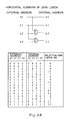
- Figures 5A to 5D illustrate three examples of data access according to the shifted diagonal system.
- Figures 5B, 5C and 5D illustrate first, second and third examples of methods of reading data from 16 data latches DL0 to DL15 of Figure 5A, four times four bits at a time.
- the first and second examples B and C are essentially the same except that they are opposite to each other in the direction of shift.
- the example of Figure 5D can be said to be a modified shifted diagonal system in that bits are reversed two bits by two bits in the second and third data readout.
- data in the first row in DL0, DL4, DL8 and DL12 are the contents which will be read simultaneously by activating column selective line CL0.
- column selective line CL0 In the event of a failure of column selective line CL0, all bits latched as the first row data will be in error.
- the shifted diagonal systems illustrated in Figures 5B, 5C and 5D allow, when four sets of four bits are read from 16 bits separately, only one bit of failed bits in DL0, DL4, DL8 and DL12 to be read and prevent more than one bit from being read in each cycle of data readout.
- the data of the (1, 1) element is in error, but the data of the (2, 2), (3, 3) and (4, 4) elements are correct in the first period.
- the (2, 1) element is in error and the remaining (2, 3), (3, 4) and (4, 1) elements are correct.
- the (1, 3) element is in error and the remaining (2, 4), (3, 1) and (4, 2) elements are correct.
- the (1, 4) element is in error and the remaining (2, 1), (3, 2) and (4, 3) elements are correct.
- 4-bit data can be read with one bit in error.
- the one-bit error can be corrected by an external Error Correcting Circuit.
- information will be obtained which is correct in four bits. Therefore, even if the four bits in the first row of 16 bits in figures 5A are all in error, 16-bit information which is correct in all bits will be obtained from the Error Correcting Circuit as long as it operates properly in each cycle. That is, more than three of the 16 bits will be corrected. The same is true of the systems of Figure 5C and 5D.
- plural bits are output simultaneously by selecting any given word line from memory cell array blocks MA0 and MA1, MA2 and MA3, MA4 and MA5, MA6 and MA7 and any given column select line from common column select lines, and one bit is output from each of respective memory cells so as to fit the number of input/output bits of the data selector of the present semiconductor memory device from the data.
- all the bits of output data will not fail and the failure is limited to only one bit even if the word lines or column select lines fail. Therefore, this Error Correcting Circuit can be used, thereby improving the reliability of a semiconductor memory device of a multi-bit input/output configuration.
- This figure shows an example in which the present invention is applied to a DRAM having 16 memory cell arrays MA0 to MA15.
- sense amplifiers are excluded from the illustration as they are placed within memory cell arrays MA0 to MA15.
- memory cell arrays MA0 to MA15 Associated with memory cell arrays MA0 to MA15 are their respective row decoders DX0 to DX15 and row drivers DRX0 to DRX15. 16 memory cell arrays MA0 to MA15 are divided into 4 blocks for 1/4 block operation. In this block operation, a block selector BS is selected by a second pre-decoder PD2 supplied with an address input of two bits A4 and A5 and 1/4 of 16 row drivers are selectively enabled by applying outputs of second pre-decoder PD2 to the row drivers (DRX0 to DRX15). Note that for 1/8 block operation the address input to second pre-decoder PD2 is only required to have three bits.
- Second pre-decoder PD2 enables only one block data latch (for example, BDL0) to allow 16-bit data read from the enabled block to be output to data selector DS4 via block selector BS.
- data selector DS4 four bits are selected from 16 bits by first pre-decoder PD1 and outputted.
- a selected data latch circuit for example, BDL0
- Figure 7 illustrates a circuit arrangement of data selector DS4. This circuit arrangement is adapted to the modified shifted diagonal system (refer to Figure 5D. In this Figure are also illustrated exemplary circuit arrangements of data selector DS1 and pre-decoder PD which adapt the "4-bit" input/output configuration to the "1 -bit" configuration by using a method such as a bonding option and AL master slice.
- Pre-decoder PD3 receives a 2-bit address input of A0 and A1 and is arranged to provide the "4-bit" input/output configuration when a switching signal S is at a HIGH level and the "1-bit” input/output configuration at a LOW level of switching signal S, thereby converting 4-bit data to 1-bit data.
- the block data latch circuit (for example, BDL0) is comprised of 16 data latch circuits (DL0 to DL15) which are selected by address inputs A0 to A3.
- data selector DS4 selects 4 bits from 16-bit data in block data latches DL0 to DL15 and applies them to common data bus LD4.
- the shifted diagonal system of Figure 5D is used as the selection system.
- data from DL0 to DL15 belong to block data latch BDL0, not to other blocks, and the data readout of BDL0 is effectively selected by block selector BS.
- block selector BS To make this block selection, only line 4 of pre-decoder PD2 is activated to logic 0 when address inputs A4 and A5 are both at 0 so that pass transistor 15 and all other transistors provided on the right side of transistor 15 are all turned on. The contents of latches DL0 to DL15 are thereby effectively input to data selector DS4.
- data selector DS4 4 bits are selected from 16 bits by activating only one of output lines 8, 7, 6 and 5 of pre-decoder PD1 to logic 1, according to address signals A2, A3 thereto.
- pre decoder PD1 line 8 goes to 1 when A2 and A3 are both at 0, line 7 goes to 1 when A2 and A3 are at 1 and 0, respectively.
- Line 6 goes to 1 when A2 and A3 are at 0 and 1, respectively, and line 5 goes to 1 when A2 and A3 are both at 1.
- 16 pass transistors are placed in the positions illustrated. With this placement, for example, when line 8 is at a logic 1, pass transistors 16, 17, 18 and 19, connected to line 8, become ON state.
- the shifted diagonal system is implemented by data selector DS4.
- one of the common data buses 20, 21, 22 and 23 is connected to another common data bus LD1 by data selector DS1.
- the address signals A0 to A3 described above are internal addresses which are obtained by converting or scrambling external address signals A0 to A3 in accordance with the systems illustrated in Figures 9A and B.
- Figure 8 The relation between the selection of the data latches and the logical combination of the address inputs is illustrated in Figure 8. It should be noted here that address inputs A4 and A5 used for dividing the memory cell arrays are not illustrated in Figure 8 because attention is now paid to the selected block (for example, memory cell arrays MA0 to MA3, block data latch BDL0).
- Figures 9A and 9B show address scrambler circuits and truth tables for implementing them. These tables represent relationships between external addresses and internal addresses. They are implemented when the external address is sequentially incremented with A0 as its least significant bit and A3 as its most significant bit.
- A4 and A5 activate line 4 in Figure 7 when they are (0, 0) and select the output of the data latches DL0 to DL15 by applying the outputs from memory cell arrays MA0, MA1, MA2 and MA3 shown in Figure 6 to block data latch BDL0.
- data selectors are selected in the order of DL0, DL4, DL8, DL12, DL1, ... DL15.
- output line 7 is activated in Figure 7 when A3 and A2 are (0, 1), thereby selecting latches DL1, DL4, DL11 and DL14. Further, when A1 and A0 are (1, 0), a content of data latch DL11 is outputted to common data bus LD1 through output line 10.
- Figure 10 illustrates a third embodiment of the present invention.
- the present invention is applied to a DRAM in which each row decoder DX0, DX1, ..., DX7 is intervened between its respective memory cell pair MA00 and MA01, MA10 and MA11, MA20 and MA21, ..., MA70 and MA71, each pair being arranged in the row direction, and each row decoder being shared between the paired memory cell arrays.
- each row decoder DX0, DX1, ..., DX7 is intervened between its respective memory cell pair MA00 and MA01, MA10 and MA11, MA20 and MA21, ..., MA70 and MA71, each pair being arranged in the row direction, and each row decoder being shared between the paired memory cell arrays.
- corresponding word lines WL00 and WL01 in memory cell arrays MA00 and MA01 are selected by the same row address signal (A0) by using one row select driving circuit DX0.
- row select driving circuit DX0 Of column select lines corresponding to bit lines BL00 to BL0i connected to memory cells CEL00 to CEL0i which are connected to word line WL00, for example, two column select lines CL0 and CL1, are driven simultaneously so that 2-bit data is output to data latches DL2 and DL3.
- column select lines corresponding to bit lines BL0j to BL0m connected to memory cells CEL0j to CEL0m which are connected to word line WL01 for example, two column select lines CL2 and CL3 are driven simultaneously so that 2-bit data is output to data latches DL0 and DL1.
- a total of 4 bits of data is output from memory cells MA00 and MA01 to data latches DL0 to DL3.
- the selected word lines WL00 and WL01 have the same address, yet they are not the same address lines and they are mutually independent.
- Figure 11 illustrates a fourth embodiment of the present invention.
- the column select lines are divided into global column select lines (GCL0, GCL1, GCL2,...GCLm) and local column select lines (LCL00, LCL0i, LCL0j, LCL0m, LCL10, LCL1i, LCL1j, LCL1m) and each of the local column select lines is connected to a corresponding global column select line via a switch (SW00, SW0i, SW0j, SWOm, SW10, SW1i, SW1j, SW1m).
- the column selective drive circuit (DY0, DY1, DY2, DY3) is further provided with a spare column decoder (hereinafter referred to as a redundant column decoder, refer to Figure 12) for a failing column select line or column decoder and each memory cell array (MA00 to MA0M, MA10 to MA1m) is provided with a spare memory cell array (hereinafter referred to as a redundant memory cell array, not shown) for failing memory cells.
- a redundant column decoder hereinafter referred to as a redundant column decoder, refer to Figure 12
- each memory cell array MA00 to MA0M, MA10 to MA1m
- a redundant memory cell array hereinafter referred to as a redundant memory cell array, not shown
- the redundant memory cells are selected by the redundant column decoder.
- the fourth embodiment is an example in which the present invention is applied to such a DRAM as described above and a modification of the third embodiment of Figure 10.
- Like reference characters are used to designate parts corresponding to those in Figure 10.
- corresponding word lines WL00 and WL01 in memory cell arrays MA00 and MA01 are selected by row selective drive circuit DX0 and data are read from memory cells CEL00 to CEL0m connected to word lines WL00 and WL01 onto their respective bit lines BL00 to BL0m.
- DX0 row selective drive circuit
- four global column select lines GCL0, GCL1, GCL2 and GCL3 may be selected simultaneously from among the column select lines and local column select lines LCL00, LCL0i, LCL0J and LCL0m selected through switches SW00, SW0i, SW0j and SW0m allow data to be latched by data latches DL0, DL1, DL2 and DL3 through BUS.
- the fourth embodiment is the same as the third embodiment in that 4 bits are finally output from 16-bit data read from four blocks one bit at a time from each block by the data selectors in accordance with the shifted diagonal method as shown in Figure 5D. These 4 bits are output by different word lines and different local column select lines, thus permitting the use of the 1-bit Error Correcting Circuit.
- the local column select line is made by using a third wiring layer in the multilayer interconnection and is shared among plural memory cell arrays (for example, MA00, MA10, MA20).
- a third wiring layer in the multilayer interconnection is shared among plural memory cell arrays (for example, MA00, MA10, MA20).
- the second wiring layer in the multilayer interconnection may be used instead without being shared among memory cell arrays.
- Each of the column decoders (DY0 to DY3) of the semiconductor memory device has a redundant column decoder (refer to Figure 12) and each of the memory cell arrays also has redundant memory cells corresponding to the redundant column decoders.
- the redundant memory cells are excluded from illustration because they are the same in arrangement and number as ordinary memory cells.
- Figure 12 illustrates the detail of a column decoder (DY0 by way of example) and means for switching to defective address inputs.
- a column decoder (DY0 by way of example) and means for switching to defective address inputs.
- CDY0 to CDYm which operate when normal address inputs for reading normal memory cells
- CRDY0 redundant column decoder
- a comparison is made between an address signal (10) obtained by amplifying an externally applied address signal (A0 to Am) by address buffer (ADB) and defective address signal (20) output from a defective address storing ROM (ROM) in which defective addresses are stored in advance by a comparator (COM).
- ADB address buffer
- ROM defective address storing ROM
- COM comparator
- each column decoder (CDY0 to CDYm) is disabled by an output (30) of the comparator (COM) and redundant column decoder (CRDY0) is thereby enabled to select redundant global column select line (GRCL0). That is, when a defective address signal is entered, the redundant decoder is enabled and the corresponding redundant memory cell (not shown) is selected. Therefore, the memory device is viewed from outside as if there were no defect.
- the switching of column select lines corresponding to defective memory cells to redundant column select lines in order to save the defective memory cells is also effective against row select lines and is thus generally executed.
- it is normal to detect defective addresses for each memory cell array (for example, MA00), store them in a defective address storage ROM and determine defective addresses for each of the memory cell arrays.
- the column select line is doubled and thus even if two column select lines fail, one bit error output can be obtained according to the present invention, thereby permitting the use of the Error Correcting Circuit.
Landscapes
- Engineering & Computer Science (AREA)
- Microelectronics & Electronic Packaging (AREA)
- Computer Hardware Design (AREA)
- Dram (AREA)
- For Increasing The Reliability Of Semiconductor Memories (AREA)
- Semiconductor Memories (AREA)
Applications Claiming Priority (2)
| Application Number | Priority Date | Filing Date | Title |
|---|---|---|---|
| JP14341389 | 1989-06-06 | ||
| JP143413/89 | 1989-06-06 |
Publications (3)
| Publication Number | Publication Date |
|---|---|
| EP0401792A2 true EP0401792A2 (de) | 1990-12-12 |
| EP0401792A3 EP0401792A3 (de) | 1992-02-26 |
| EP0401792B1 EP0401792B1 (de) | 1996-01-17 |
Family
ID=15338191
Family Applications (1)
| Application Number | Title | Priority Date | Filing Date |
|---|---|---|---|
| EP90110712A Expired - Lifetime EP0401792B1 (de) | 1989-06-06 | 1990-06-06 | Halbleiterspeicheranordnung |
Country Status (5)
| Country | Link |
|---|---|
| US (1) | US5502675A (de) |
| EP (1) | EP0401792B1 (de) |
| JP (1) | JPH0814985B2 (de) |
| KR (1) | KR970004996B1 (de) |
| DE (1) | DE69024851T2 (de) |
Cited By (10)
| Publication number | Priority date | Publication date | Assignee | Title |
|---|---|---|---|---|
| EP0577106A3 (en) * | 1992-06-30 | 1994-06-01 | Nec Corp | Semiconductor memory circuit |
| EP0678872A1 (de) * | 1994-04-13 | 1995-10-25 | Kabushiki Kaisha Toshiba | Halbleiterspeicheranordnung |
| EP0795875A3 (de) * | 1996-03-11 | 1999-11-10 | Kabushiki Kaisha Toshiba | Speicheranordnung mit überlagerter Busstruktur |
| EP0902434A3 (de) * | 1997-09-11 | 1999-12-08 | International Business Machines Corporation | Hierarchische Spaltenleitungsauswahl für Multi-Bank-DRAM-Speicher und Verfahren dazu |
| US6084817A (en) * | 1996-03-11 | 2000-07-04 | Kabushiki Kaisha Toshiba | Semiconductor memory with transfer buffer structure |
| EP1081711A2 (de) | 1994-09-22 | 2001-03-07 | Kabushiki Kaisha Toshiba | Dynamischer Speicher |
| EP1394808A3 (de) * | 2002-08-29 | 2004-06-23 | Fujitsu Limited | Halbleiterspeicheranordnung |
| EP2062264A4 (de) * | 2006-07-31 | 2010-11-10 | Sandisk 3D Llc | Verfahren 8nd vorrichtung für einen speichert mit zwei datenbussen zur speicherblockauswahl |
| US8004927B2 (en) | 2006-07-31 | 2011-08-23 | Sandisk 3D Llc | Reversible-polarity decoder circuit and method |
| US8279704B2 (en) | 2006-07-31 | 2012-10-02 | Sandisk 3D Llc | Decoder circuitry providing forward and reverse modes of memory array operation and method for biasing same |
Families Citing this family (43)
| Publication number | Priority date | Publication date | Assignee | Title |
|---|---|---|---|---|
| JPH06195973A (ja) * | 1992-10-12 | 1994-07-15 | Nec Corp | ダイナミックram |
| US5812478A (en) * | 1995-01-05 | 1998-09-22 | Kabushiki Kaisha Toshiba | Semiconductor memory having improved data bus arrangement |
| JP3267462B2 (ja) * | 1995-01-05 | 2002-03-18 | 株式会社東芝 | 半導体記憶装置 |
| US5943693A (en) * | 1995-03-29 | 1999-08-24 | Intel Corporation | Algorithmic array mapping to decrease defect sensitivity of memory devices |
| JPH0973778A (ja) * | 1995-09-01 | 1997-03-18 | Texas Instr Japan Ltd | アドレスアクセスパスのコントロール回路 |
| JPH09161476A (ja) * | 1995-10-04 | 1997-06-20 | Toshiba Corp | 半導体メモリ及びそのテスト回路、並びにデ−タ転送システム |
| US6072719A (en) | 1996-04-19 | 2000-06-06 | Kabushiki Kaisha Toshiba | Semiconductor memory device |
| US5815456A (en) * | 1996-06-19 | 1998-09-29 | Cirrus Logic, Inc. | Multibank -- multiport memories and systems and methods using the same |
| JPH1050958A (ja) * | 1996-08-05 | 1998-02-20 | Toshiba Corp | 半導体記憶装置、半導体記憶装置のレイアウト方法、半導体記憶装置の動作方法および半導体記憶装置の回路配置パターン |
| US5781483A (en) * | 1996-12-31 | 1998-07-14 | Micron Technology, Inc. | Device and method for repairing a memory array by storing each bit in multiple memory cells in the array |
| US5822268A (en) * | 1997-09-11 | 1998-10-13 | International Business Machines Corporation | Hierarchical column select line architecture for multi-bank DRAMs |
| US6034914A (en) * | 1997-10-30 | 2000-03-07 | Kabushiki Kaisha Toahiba | Semiconductor memory device having column redundancy function |
| US5907511A (en) * | 1997-12-23 | 1999-05-25 | Lsi Logic Corporation | Electrically selectable redundant components for an embedded DRAM |
| US5901095A (en) * | 1997-12-23 | 1999-05-04 | Lsi Logic Corporation | Reprogrammable address selector for an embedded DRAM |
| US5896331A (en) * | 1997-12-23 | 1999-04-20 | Lsi Logic Corporation | Reprogrammable addressing process for embedded DRAM |
| KR19990061991A (ko) * | 1997-12-31 | 1999-07-26 | 김영환 | 다수개의 리던던시 입출력 라인들을 구비하는 반도체 장치 |
| US6246630B1 (en) | 1998-02-02 | 2001-06-12 | International Business Machines Corporation | Intra-unit column address increment system for memory |
| US6118726A (en) * | 1998-02-02 | 2000-09-12 | International Business Machines Corporation | Shared row decoder |
| US6002275A (en) * | 1998-02-02 | 1999-12-14 | International Business Machines Corporation | Single ended read write drive for memory |
| US6038634A (en) * | 1998-02-02 | 2000-03-14 | International Business Machines Corporation | Intra-unit block addressing system for memory |
| US5999440A (en) * | 1998-03-30 | 1999-12-07 | Lsi Logic Corporation | Embedded DRAM with noise-protecting substrate isolation well |
| US6064588A (en) * | 1998-03-30 | 2000-05-16 | Lsi Logic Corporation | Embedded dram with noise-protected differential capacitor memory cells |
| US6049505A (en) | 1998-05-22 | 2000-04-11 | Micron Technology, Inc. | Method and apparatus for generating memory addresses for testing memory devices |
| US6005824A (en) * | 1998-06-30 | 1999-12-21 | Lsi Logic Corporation | Inherently compensated clocking circuit for dynamic random access memory |
| US5978304A (en) * | 1998-06-30 | 1999-11-02 | Lsi Logic Corporation | Hierarchical, adaptable-configuration dynamic random access memory |
| US6115300A (en) * | 1998-11-03 | 2000-09-05 | Silicon Access Technology, Inc. | Column redundancy based on column slices |
| JP2000182390A (ja) | 1998-12-11 | 2000-06-30 | Mitsubishi Electric Corp | 半導体記憶装置 |
| KR100351048B1 (ko) * | 1999-04-27 | 2002-09-09 | 삼성전자 주식회사 | 데이터 입출력 라인의 부하를 최소화하는 칼럼 선택 회로, 이를 구비하는 반도체 메모리 장치 |
| US6477082B2 (en) * | 2000-12-29 | 2002-11-05 | Micron Technology, Inc. | Burst access memory with zero wait states |
| US6549476B2 (en) | 2001-04-09 | 2003-04-15 | Micron Technology, Inc. | Device and method for using complementary bits in a memory array |
| JP5119563B2 (ja) * | 2001-08-03 | 2013-01-16 | 日本電気株式会社 | 不良メモリセル救済回路を有する半導体記憶装置 |
| US20030163769A1 (en) * | 2002-02-27 | 2003-08-28 | Sun Microsystems, Inc. | Memory module including an error detection mechanism for address and control signals |
| US6941493B2 (en) * | 2002-02-27 | 2005-09-06 | Sun Microsystems, Inc. | Memory subsystem including an error detection mechanism for address and control signals |
| US6996766B2 (en) * | 2002-06-28 | 2006-02-07 | Sun Microsystems, Inc. | Error detection/correction code which detects and corrects a first failing component and optionally a second failing component |
| US6976194B2 (en) * | 2002-06-28 | 2005-12-13 | Sun Microsystems, Inc. | Memory/Transmission medium failure handling controller and method |
| US6973613B2 (en) * | 2002-06-28 | 2005-12-06 | Sun Microsystems, Inc. | Error detection/correction code which detects and corrects component failure and which provides single bit error correction subsequent to component failure |
| US6996686B2 (en) * | 2002-12-23 | 2006-02-07 | Sun Microsystems, Inc. | Memory subsystem including memory modules having multiple banks |
| US7779285B2 (en) * | 2003-02-18 | 2010-08-17 | Oracle America, Inc. | Memory system including independent isolated power for each memory module |
| US7530008B2 (en) | 2003-08-08 | 2009-05-05 | Sun Microsystems, Inc. | Scalable-chip-correct ECC scheme |
| US7188296B1 (en) | 2003-10-30 | 2007-03-06 | Sun Microsystems, Inc. | ECC for component failures using Galois fields |
| US20060182187A1 (en) * | 2005-02-11 | 2006-08-17 | Likovich Robert B Jr | Automatic reconfiguration of an I/O bus to correct for an error bit |
| JP5018074B2 (ja) | 2006-12-22 | 2012-09-05 | 富士通セミコンダクター株式会社 | メモリ装置,メモリコントローラ及びメモリシステム |
| US20080309532A1 (en) * | 2007-06-12 | 2008-12-18 | Silicon Optronics, Inc. | Solid-state imaging device and method of manufacturing thereof |
Family Cites Families (24)
| Publication number | Priority date | Publication date | Assignee | Title |
|---|---|---|---|---|
| US4006467A (en) * | 1975-11-14 | 1977-02-01 | Honeywell Information Systems, Inc. | Error-correctible bit-organized RAM system |
| JPS5298433A (en) * | 1976-02-16 | 1977-08-18 | Hitachi Ltd | Semiconductor memory |
| JPS57198592A (en) * | 1981-05-29 | 1982-12-06 | Hitachi Ltd | Semiconductor memory device |
| JPS58139399A (ja) * | 1982-02-15 | 1983-08-18 | Hitachi Ltd | 半導体記憶装置 |
| US4943967A (en) * | 1982-02-15 | 1990-07-24 | Hitachi, Ltd. | Semiconductor memory with an improved dummy cell arrangement and with a built-in error correction code circuit |
| US4483001A (en) * | 1982-06-16 | 1984-11-13 | International Business Machines Corporation | Online realignment of memory faults |
| JPS5975494A (ja) * | 1982-10-25 | 1984-04-28 | Hitachi Ltd | 半導体記憶装置 |
| JPS60179859A (ja) * | 1984-02-27 | 1985-09-13 | Nippon Telegr & Teleph Corp <Ntt> | 半導体記憶装置 |
| JPS6180597A (ja) * | 1984-09-26 | 1986-04-24 | Hitachi Ltd | 半導体記憶装置 |
| US4692923A (en) * | 1984-09-28 | 1987-09-08 | Ncr Corporation | Fault tolerant memory |
| JPS61105800A (ja) * | 1984-10-29 | 1986-05-23 | Nec Corp | 半導体メモリ |
| JPH0652632B2 (ja) * | 1985-01-23 | 1994-07-06 | 株式会社日立製作所 | ダイナミツク型ram |
| JPS6247900A (ja) * | 1985-08-27 | 1987-03-02 | Toshiba Corp | メモリ装置 |
| US4747080A (en) * | 1985-11-12 | 1988-05-24 | Nippon Telegraph & Telephone Corporation | Semiconductor memory having self correction function |
| JPS62134899A (ja) * | 1985-12-06 | 1987-06-17 | Mitsubishi Electric Corp | 半導体記憶装置 |
| JPH0612613B2 (ja) * | 1986-03-18 | 1994-02-16 | 富士通株式会社 | 半導体記憶装置 |
| JPS62250600A (ja) * | 1986-04-22 | 1987-10-31 | Sharp Corp | 半導体集積回路装置 |
| JPS63239675A (ja) * | 1986-11-27 | 1988-10-05 | Toshiba Corp | 半導体記憶装置 |
| JPS63140493A (ja) * | 1986-12-01 | 1988-06-13 | Mitsubishi Electric Corp | 半導体記憶装置 |
| JPS63204600A (ja) * | 1987-02-18 | 1988-08-24 | Mitsubishi Electric Corp | 半導体記憶装置 |
| JP2629697B2 (ja) * | 1987-03-27 | 1997-07-09 | 日本電気株式会社 | 半導体記憶装置 |
| JPS63304496A (ja) * | 1987-06-03 | 1988-12-12 | Mitsubishi Electric Corp | 半導体記憶装置 |
| JPS6457495A (en) * | 1987-08-28 | 1989-03-03 | Hitachi Ltd | Semiconductor memory device |
| JPH0752583B2 (ja) * | 1987-11-30 | 1995-06-05 | 株式会社東芝 | 半導体メモリ |
-
1990
- 1990-06-01 JP JP2141650A patent/JPH0814985B2/ja not_active Expired - Lifetime
- 1990-06-06 DE DE69024851T patent/DE69024851T2/de not_active Expired - Fee Related
- 1990-06-06 EP EP90110712A patent/EP0401792B1/de not_active Expired - Lifetime
- 1990-06-07 KR KR1019900008353A patent/KR970004996B1/ko not_active Expired - Fee Related
-
1994
- 1994-06-04 US US08/254,412 patent/US5502675A/en not_active Expired - Lifetime
Cited By (20)
| Publication number | Priority date | Publication date | Assignee | Title |
|---|---|---|---|---|
| US5444305A (en) * | 1992-06-30 | 1995-08-22 | Nec Corporation | Semiconductor memory circuit |
| USRE36203E (en) * | 1992-06-30 | 1999-04-27 | Nec Corporation | Semiconductor memory circuit |
| EP0577106A3 (en) * | 1992-06-30 | 1994-06-01 | Nec Corp | Semiconductor memory circuit |
| EP0678872A1 (de) * | 1994-04-13 | 1995-10-25 | Kabushiki Kaisha Toshiba | Halbleiterspeicheranordnung |
| US5590084A (en) * | 1994-04-13 | 1996-12-31 | Kabushiki Kaisha Toshiba | Semiconductor memory device having a column selector |
| EP1081711A2 (de) | 1994-09-22 | 2001-03-07 | Kabushiki Kaisha Toshiba | Dynamischer Speicher |
| EP1081711A3 (de) * | 1994-09-22 | 2008-04-09 | Kabushiki Kaisha Toshiba | Dynamischer Speicher |
| EP0795875A3 (de) * | 1996-03-11 | 1999-11-10 | Kabushiki Kaisha Toshiba | Speicheranordnung mit überlagerter Busstruktur |
| US6084817A (en) * | 1996-03-11 | 2000-07-04 | Kabushiki Kaisha Toshiba | Semiconductor memory with transfer buffer structure |
| US6219295B1 (en) | 1996-03-11 | 2001-04-17 | Kabushiki Kaisha Toshiba | Semiconductor memory with transfer buffer structure |
| US6396765B2 (en) | 1996-03-11 | 2002-05-28 | Kabushiki Kaisha Toshiba | Semiconductor memory having an overlaid bus structure |
| US6469951B2 (en) | 1996-03-11 | 2002-10-22 | Kabushiki Kaisha Toshiba | Semiconductor memory having an overlaid bus structure |
| KR100305937B1 (ko) * | 1997-09-11 | 2001-10-19 | 포만 제프리 엘 | 동적랜덤액세스메모리및그구성방법 |
| EP0902434A3 (de) * | 1997-09-11 | 1999-12-08 | International Business Machines Corporation | Hierarchische Spaltenleitungsauswahl für Multi-Bank-DRAM-Speicher und Verfahren dazu |
| EP1394808A3 (de) * | 2002-08-29 | 2004-06-23 | Fujitsu Limited | Halbleiterspeicheranordnung |
| US6831870B2 (en) | 2002-08-29 | 2004-12-14 | Fujitsu Limited | Semiconductor memory |
| EP2062264A4 (de) * | 2006-07-31 | 2010-11-10 | Sandisk 3D Llc | Verfahren 8nd vorrichtung für einen speichert mit zwei datenbussen zur speicherblockauswahl |
| US8004927B2 (en) | 2006-07-31 | 2011-08-23 | Sandisk 3D Llc | Reversible-polarity decoder circuit and method |
| US8279704B2 (en) | 2006-07-31 | 2012-10-02 | Sandisk 3D Llc | Decoder circuitry providing forward and reverse modes of memory array operation and method for biasing same |
| US8509025B2 (en) | 2006-07-31 | 2013-08-13 | Sandisk 3D Llc | Memory array circuit incorporating multiple array block selection and related method |
Also Published As
| Publication number | Publication date |
|---|---|
| EP0401792B1 (de) | 1996-01-17 |
| DE69024851T2 (de) | 1996-09-05 |
| JPH0386992A (ja) | 1991-04-11 |
| EP0401792A3 (de) | 1992-02-26 |
| JPH0814985B2 (ja) | 1996-02-14 |
| DE69024851D1 (de) | 1996-02-29 |
| KR970004996B1 (ko) | 1997-04-10 |
| US5502675A (en) | 1996-03-26 |
| KR910001769A (ko) | 1991-01-31 |
Similar Documents
| Publication | Publication Date | Title |
|---|---|---|
| US5502675A (en) | Semiconductor memory device having a multi-bit input/output configuration which is capable of correcting a bit failure | |
| US5400342A (en) | Semiconductor memory having test circuit and test method thereof | |
| US5617364A (en) | Semiconductor memory device | |
| US6459630B2 (en) | Semiconductor memory device having replacing defective columns with redundant columns | |
| US5386386A (en) | Redundancy circuit having a spare memory block replacing defective memory cells in different blocks | |
| US20020024859A1 (en) | Semiconductor memory device having a large band width and allowing efficient execution of redundant repair | |
| EP0615252B1 (de) | Halbleiterspeicher mit eingebautem parallelen Bitprüfmodus | |
| US4916700A (en) | Semiconductor storage device | |
| US5436911A (en) | Semiconductor memory device comprising a test circuit and a method of operation thereof | |
| US5446692A (en) | Semiconductor memory device having redundancy memory cells shared among memory blocks | |
| US6490210B2 (en) | Semiconductor memory integrated circuit employing a redundant circuit system for compensating for defectiveness | |
| US6307794B1 (en) | Semiconductor memory device and signal line shifting method | |
| US6055196A (en) | Semiconductor device with increased replacement efficiency by redundant memory cell arrays | |
| JP4504558B2 (ja) | 半導体集積メモリ | |
| US5272672A (en) | Semiconductor memory device having redundant circuit | |
| US6469949B1 (en) | Fuse latch array system for an embedded DRAM having a micro-cell architecture | |
| US4937790A (en) | Semiconductor memory device | |
| US5452258A (en) | Semiconductor read only memory | |
| US6985395B2 (en) | Semiconductor memory device and method of testing the device | |
| US5305258A (en) | Semiconductor memory and memory cell | |
| US20030133320A1 (en) | Twisted bit-line compensation | |
| US6809972B2 (en) | Circuit technique for column redundancy fuse latches | |
| US7117400B2 (en) | Memory device with data line steering and bitline redundancy | |
| US7146456B2 (en) | Memory device with a flexible reduced density option | |
| US5901093A (en) | Redundancy architecture and method for block write access cycles permitting defective memory line replacement |
Legal Events
| Date | Code | Title | Description |
|---|---|---|---|
| PUAI | Public reference made under article 153(3) epc to a published international application that has entered the european phase |
Free format text: ORIGINAL CODE: 0009012 |
|
| AK | Designated contracting states |
Kind code of ref document: A2 Designated state(s): DE FR GB |
|
| PUAL | Search report despatched |
Free format text: ORIGINAL CODE: 0009013 |
|
| AK | Designated contracting states |
Kind code of ref document: A3 Designated state(s): DE FR GB |
|
| 17P | Request for examination filed |
Effective date: 19920520 |
|
| 17Q | First examination report despatched |
Effective date: 19931210 |
|
| GRAA | (expected) grant |
Free format text: ORIGINAL CODE: 0009210 |
|
| AK | Designated contracting states |
Kind code of ref document: B1 Designated state(s): DE FR GB |
|
| REF | Corresponds to: |
Ref document number: 69024851 Country of ref document: DE Date of ref document: 19960229 |
|
| ET | Fr: translation filed | ||
| PLBE | No opposition filed within time limit |
Free format text: ORIGINAL CODE: 0009261 |
|
| STAA | Information on the status of an ep patent application or granted ep patent |
Free format text: STATUS: NO OPPOSITION FILED WITHIN TIME LIMIT |
|
| 26N | No opposition filed | ||
| REG | Reference to a national code |
Ref country code: GB Ref legal event code: IF02 |
|
| PGFP | Annual fee paid to national office [announced via postgrant information from national office to epo] |
Ref country code: GB Payment date: 20050601 Year of fee payment: 16 |
|
| PGFP | Annual fee paid to national office [announced via postgrant information from national office to epo] |
Ref country code: DE Payment date: 20050602 Year of fee payment: 16 |
|
| PGFP | Annual fee paid to national office [announced via postgrant information from national office to epo] |
Ref country code: FR Payment date: 20050608 Year of fee payment: 16 |
|
| PG25 | Lapsed in a contracting state [announced via postgrant information from national office to epo] |
Ref country code: GB Free format text: LAPSE BECAUSE OF NON-PAYMENT OF DUE FEES Effective date: 20060606 |
|
| PG25 | Lapsed in a contracting state [announced via postgrant information from national office to epo] |
Ref country code: DE Free format text: LAPSE BECAUSE OF NON-PAYMENT OF DUE FEES Effective date: 20070103 |
|
| GBPC | Gb: european patent ceased through non-payment of renewal fee |
Effective date: 20060606 |
|
| REG | Reference to a national code |
Ref country code: FR Ref legal event code: ST Effective date: 20070228 |
|
| PG25 | Lapsed in a contracting state [announced via postgrant information from national office to epo] |
Ref country code: FR Free format text: LAPSE BECAUSE OF NON-PAYMENT OF DUE FEES Effective date: 20060630 |