EP0397239B1 - Schaltungsanordnung zum Liefern eines periodischen, im wesentlichen parabelförmigen Signals - Google Patents
Schaltungsanordnung zum Liefern eines periodischen, im wesentlichen parabelförmigen Signals Download PDFInfo
- Publication number
- EP0397239B1 EP0397239B1 EP90201095A EP90201095A EP0397239B1 EP 0397239 B1 EP0397239 B1 EP 0397239B1 EP 90201095 A EP90201095 A EP 90201095A EP 90201095 A EP90201095 A EP 90201095A EP 0397239 B1 EP0397239 B1 EP 0397239B1
- Authority
- EP
- European Patent Office
- Prior art keywords
- signal
- arcuate
- periods
- during
- retrace
- Prior art date
- Legal status (The legal status is an assumption and is not a legal conclusion. Google has not performed a legal analysis and makes no representation as to the accuracy of the status listed.)
- Expired - Lifetime
Links
- 230000000737 periodic effect Effects 0.000 title claims 4
- 239000003990 capacitor Substances 0.000 claims description 40
- 238000005070 sampling Methods 0.000 description 11
- 238000010586 diagram Methods 0.000 description 6
- 230000001419 dependent effect Effects 0.000 description 2
- 238000001514 detection method Methods 0.000 description 2
- 230000007704 transition Effects 0.000 description 2
- 230000006978 adaptation Effects 0.000 description 1
- 230000015572 biosynthetic process Effects 0.000 description 1
- 238000010276 construction Methods 0.000 description 1
- 230000004069 differentiation Effects 0.000 description 1
- 230000009977 dual effect Effects 0.000 description 1
- 230000000694 effects Effects 0.000 description 1
- 230000010354 integration Effects 0.000 description 1
- 238000000034 method Methods 0.000 description 1
- 238000004088 simulation Methods 0.000 description 1
- 238000003786 synthesis reaction Methods 0.000 description 1
Images


Classifications
-
- H—ELECTRICITY
- H03—ELECTRONIC CIRCUITRY
- H03K—PULSE TECHNIQUE
- H03K4/00—Generating pulses having essentially a finite slope or stepped portions
- H03K4/06—Generating pulses having essentially a finite slope or stepped portions having triangular shape
-
- H—ELECTRICITY
- H03—ELECTRONIC CIRCUITRY
- H03K—PULSE TECHNIQUE
- H03K4/00—Generating pulses having essentially a finite slope or stepped portions
- H03K4/02—Generating pulses having essentially a finite slope or stepped portions having stepped portions, e.g. staircase waveform
- H03K4/023—Generating pulses having essentially a finite slope or stepped portions having stepped portions, e.g. staircase waveform by repetitive charge or discharge of a capacitor, analogue generators
-
- H—ELECTRICITY
- H03—ELECTRONIC CIRCUITRY
- H03K—PULSE TECHNIQUE
- H03K4/00—Generating pulses having essentially a finite slope or stepped portions
- H03K4/04—Generating pulses having essentially a finite slope or stepped portions having parabolic shape
Definitions
- the invention relates to a circuit arrangement as defined in the precharacterizing part of claim 1.
- a circuit arrangement of this type is known from EP-A-0,273,497 (PHN 11.964) and is used, for example, for generating a substantially parabolic control signal of an east-west modulator in a picture display device and/or for a dynamic focusing in such an arrangement.
- This control signal may have the field frequency (50 Hz in accordance with the European standard) or the line frequency (15.625 kHz in accordance with the said standard) or any other suitable frequency.
- the known circuit arrangement ensures that a arcuate signal portion and a substantially parabolic signal portion and their derivatives with respect to time continuously merge.
- this is achieved in that the arcuate signal portion and its derivative with respect to time are given values at a start of a retrace period corresponding to the values of the substantially parabolic signal portion and its derivative at the end of the trace period.
- the natural frequency of the arcuate signal portion is chosen to be such that the arcuate signal portion and its derivative assume values at the end of the retrace period corresponding to the values of the substantially parabolic signal portion at the start of the trace period.
- a drawback of the known circuit arrangement is that it is not very well possible to vary the duration of the retrace period because then the continuity between the arcuate signal portion and the substantially parabolic signal portion at the end of the retrace period is lost. It is often desirable that the retrace period should be variable or adjustable, for example, in multi-standard picture display devices, or that the centring of the displayed picture should be adjustable.
- a DC component is added so that the centre of the picture information is displayed in a centre of a display screen. If this offset sawtooth signal is squared for the purpose of east-west correction, a parabola is produced with a start and an end not being at the same level. This is undesirable because a symmetrical east-west correction is necessary.
- the trace period is therefore preferably varied so that the picture information is also offset on the display screen. However, this produces an opposite variation of the retrace period.
- the invention provides a circuit arrangement as defined in Claim 1.
- Advantageous embodiments are defined in the dependent Claims.
- the substantially parabolic signal portion generated by the circuit arrangement is substantially continuous at arbitrary ratios between trace period and retrace period, thus generally at arbitrary values of the retrace period.
- the circuit arrangement according to the invention is simple and monolithically integrable.
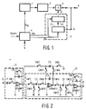
- Fig. 1 is a basic circuit diagram of the circuit arrangement according to the invention.
- a sawtooth generator 1 generates a sawtooth signal which comprises in known manner a trace and a retrace. This sawtooth signal is applied to a parabolic generator 2 which converts this signal, at least during the trace, by means of squaring to a parabolic signal for the east-west correction. This parabolic signal is applied to an adder circuit 5.
- An arcuate signal generator 3 generates an arcuate signal during the retrace and this arcuate signal is applied via an output B to the adder circuit 5 which adds this arcuate signal to the parabolic signal.
- a signal is available at the output D of the adder circuit, which signal comprises the parabolic signal from the parabolic generator 2 during the trace time and the arcuate signal originating from the arcuate signal generator during the retrace time.
- This output signal may be used, for example, for the east-west correction.
- the retrace time can be varied.
- the arcuate signal generator has such a construction that, independent of the duration of the retrace time, the parabolic signal and the arcuate signal always continuously merge and that the derivatives of the two signals also continuously merge.
- the arcuate signal generator 3 comprises a differentiator 31 and an arcuate waveform generator 32.
- the differentiator 31 which is connected to the output of the adder circuit 5 via an input A and which thus receives the parabolic signal, determines the derivative of the parabolic signal at the end of the trace and applies this derivative to the arcuate waveform generator 32.
- the arcuate waveform generator uses this derivative for generating an arcuate signal whose value and its derivative at the start of the retrace time are contiguous to that of the parabolic signal at the end of the trace time.
- the input A of the differentiator 31 may of course also be connected to the output of the parabolic generator 2.
- the sawtooth generator 1 and the arcuate signal generator 3 are controlled by a pulse circuit 4 which receives the field-synchronizing pulse Vsync and a control signal N which is a measure of correcting the centration. With reference to the signal Vsync the pulse circuit 4 determines the starting instant of the retrace time and with reference to the two input signals the pulse circuit determines the starting instant of the trace time of the sawtooth signal.
- Fig. 2 shows an embodiment of the arcuate signal generator in which the corresponding elements of Fig. 1 have the same reference numerals.
- This arcuate signal generator comprises switched capacitors.
- Fig. 2 shows a plurality of switches all of which are controlled from the pulse circuit 4 via an input C in a manner which is not further shown in this Figure.
- Fig. 2a shows the switching phases of these switches.
- the period in which the switches are switched is subdivided into the retrace time and the trace time.
- a signal STSC indicates this subdivision and during the retrace time this signal is high (1) and during the trace time it is low (0). High implies that the switches are closed and low implies that they are open.
- the switches SW1 and SW3 switch synchronously during the trace time and are closed during sampling periods ts, while they are open between these sampling periods and during the retrace time.
- the switch SW2 switches in phase opposition with respect to the switches SW1 and SW3.
- the switches SW4 and SW15 are closed during the entire trace time and open during the entire retrace time.
- the switches SW5 and SW6 switch in phase opposition with the switches SW4 and SW15.
- the switches SW7, SW8 and SW12 switch synchronously during the retrace time and close and open periodically, while they are closed during periods tf and open during the intermediate periods which are preferably as long as the periods tf. These switches are open during the trace time.
- the switches SW9, SW10 and SW14 switch in phase opposition with the switches SW7, SW8 and SW12.
- the switch SW11 switches synchronously with the switches SW9, SW10 and SW14 during the retrace time and is open during the entire trace time.
- the switch SW13 switches synchronously with the switches SW7, SW8 and SW12 during the retrace time and is closed during the entire trace time.
- Fig. 2a shows a too low number of pulses during the trace time and during the retrace time. In practice these numbers are usually much larger.
- the parabolic signal is received at the input A of Fig. 2 during the trace time.
- this signal is differentiated in the differentiator 31.
- the differentiator includes a capacitor C1 a terminal of which is connected to the input A and the other terminal of which is connected to one side of a switch SW1, while the other side of this switch is connected to an inverting input of an operational amplifier OPAMP1.
- the non-inverting input of the operational amplifier is connected to ground.
- sampling period ts the switch SW1 is closed and during the rest of the period it is open.
- the inverting input of the operational amplifier OPAMP1 is also connected to an output of this amplifier via a second capacitor C2.
- a second switch SW2 which is open during the sampling periods and is closed during the rest of the period is arranged parallel to this capacitor.
- the input signal is present across the capacitor C1 because the inverting input of the operational amplifier is virtually connected to ground. Since the capacitor C2 is short-circuited after each sampling, the derivative of the input signal is obtained at the output of the operational amplifier OPAMP1, the derivative being multiplied by a factor of P*C1/C2.
- the value P is the ratio between the duration of the period of the switching pulses during the trace time (PT) and the duration of the period of the switching pulses during the retrace time.
- the pulse circuit of Fig. 1 provides this fixed ratio between the duration of the period of the switching pulses during the trace time and the duration of the period of the switching pulses during the retrace time.
- This derivative is required as an input signal for the arcuate waveform generator 32 which generates the arcuate signal.
- the sampling of the derivative is stored via a switch SW3 in a third capacitor C5 which is connected to the output of the operational amplifier OPAMP1.
- the switch SW3 is closed and opened synchronously with the switch SW1.
- the other terminal of the capacitor C5 is connected to ground via a switch SW4 throughout the trace time.
- the arcuate waveform generator comprises two integrators. This arcuate waveform generator receives the derivative of the parabolic signal at the start of the retrace time, which signal is obtained by means of the capacitor C5 which is parallel to a capacitor C4 via two switches SW5 and SW6 during the retrace. A terminal of the capacitor C4 is connected to an inverting input of a second operational amplifier OPAMP2 and the other terminal is connected to the output of the operational amplifier OPAMP2. This capacitor C4 is required to prevent this amplifier from getting into an open loop during the trace time when the switches SW5 and SW6 are open.
- the output of the operational amplifier OPAMP2 is connected to a capacitor C6 via a switch SW11 which is periodically opened during the periods tf and closed during the intermediate periods.
- the junction point between the switch SW11 and the capacitor C6 is connected to a switch SW13 which is closed and opened synchronously with the switch SW11 but in an opposite manner, i.e. if the switch SW11 is open, the switch SW13 is closed, and vice versa.
- the other end of the switch SW13 is connected to ground.
- the other terminal of the capacitor C6 is connected to an inverting input of an operational amplifier OPAMP3 via a switch SW12.
- the switch SW12 is closed and opened synchronously with the switch SW13 during the retrace time.
- the junction point between the capacitor C6 and the switch SW12 is connected to a switch SW14 which is opened and closed synchronously with the switch SW11 and the other end of which is connected to ground.
- the non-inverting input of the operational amplifier OPAMP3 is connected to ground.
- the inverting input of this operational amplifier is connected to a capacitor C7 the other terminal of which is connected to the output of the operational amplifier, which output is also the output B of the arcuate signal generator.
- a switch SW15 which is open during the retrace time and closed during the trace time, is arranged parallel to the capacitor C7.
- the output of the operational amplifier OPAMP3 is also fed back via a switch SW7 which is connected to the inverting input of the operational amplifier OPAMP2 via a capacitor C3 and a switch SW8.
- the switches SW7 and SW8 are closed and opened synchronously with the switch SW12.
- the junction point between the switch SW7 and the capacitor C3 is connected to a switch SW9 the other end of which is connected to ground.
- the junction point between the capacitor C3 and the switch SW8 is connected to a switch SW10 the other end of which is connected to ground.
- the switches SW9 and SW10 are closed and opened synchronously with the switch SW14.
- the circuit arrangement shown in Fig. 2 starts from the parabolic signal received at the input A during the trace time, the circuit arrangement shown in Fig. 2 generates the arcuate signal.
- the arcuate signal is generated in the arcuate waveform generator by the two integrators which are each constituted by an operational amplifier and a plurality of switches.
- the first integration i.e. at the output of the operational amplifier OPAMP2
- a sinusoidal signal is produced whose phase differs ninety degrees from the sinusoidal arcuate signal which is produced at the output of the second integrator, i.e. at the output of the operational amplifier OPAMP3.
- an arcuate signal is obtained with a derivative at the start which is equal to the derivative at the end of the parabolic signal.
- the derivative at the end of the arcuate signal is always equal to the derivative at the start of the parabolic signal when varying the retrace time. If this were effected in a corresponding manner, i.e. if the derivative of the arcuate signal were determined and if it were applied to the parabolic generator for influencing the derivative at the start of the parabolic signal, this would lead to a variation of the amplitude of the parabolic signal and hence to an incorrect east-west correction.
- this can be prevented by varying the frequency of the switching pulses tf when varying the retrace time, and this in such a manner that the number of switching pulses tf during the retrace time remains constant at a given, correctly chosen value.
- Fig. 3 which is an elaborated circuit diagram of the pulse circuit 4 (of Fig. 1) will illustrate the way in which this is effected.
- the system clock having a frequency of 432 times the line frequency is applied to all components of the pulse circuit 4.
- the pulse circuit receives the field-synchronizing signal Vsync at an input, which signal originates, for example, from a sync separator which is not further shown.
- a second input of this pulse circuit receives the control signal N which is, for example, a measure of the centration.
- This signal N represents an integer indicating the number of line periods covered by the retrace and may be applied, for example, via an I2C bus.
- a first output signal Vsg of this pulse circuit controls the sawtooth generator.
- a second output signal Vsb is conveyed by a plurality of signal leads controlling the switches of the arcuate signal generator 3 in the manner shown in Fig. 2a.
- the signal Vsync is applied to a detection circuit 41 detecting the instant when a field-synchronizing signal is received.
- This detection circuit supplies a signal VR after detecting a synchronizing pulse.
- the signal VR is applied as a reset signal to a programmable frequency divider 42.
- This frequency divider receives the signal N as a second input signal which determines the division.
- the frequency divider 42 divides the system clock frequency by 6N.
- a signal Vbg having a frequency of 72/N times the line frequency is produced at the output of the frequency divider, which implies that, independent of the duration of the retrace, 72 pulses will occur during the retrace.
- the signal Vbg is applied to a counter 43 which is reset by the signal VR at the start of the retrace time and which subsequently counts 72 pulses of this signal Vbg.
- the signal STSC is produced, which is high during N line periods, i.e. the field retrace time, and which is low during the rest of the period.
- the signal STSC is the signal showing the distinction between the trace time and the retrace time in Fig. 2a.
- This signal STSC is applied to a pulse reduction circuit 44 which may be implemented in the way as is shown in the afore-mentioned European Patent Application no. 0,301,633 (PHN 12.193) and which is herein incorporated by reference.
- the pulse reduction circuit 44 supplies a fixed number of pulses during the trace time, which results in the output signal Vsg controlling the sawtooth generator.
- the signal VR operates as a reset signal also for this pulse reduction circuit 44.
- the signal STSC and the signal Vbg are also applied to a control circuit 45 which determines the switching phases (as shown in Fig. 2a) for the switches of Fig. 2 (and Fig. 4, respectively) with reference to these two signals. Particularly, this control circuit divides the frequencies in such a way that the duration of the period of the switching pulses during the trace time is P times as long as the duration of the period of the switching pulses during the retrace time.
- the reference P is the previously mentioned fixed ratio by which the derivative of the parabolic signal is multiplied in such a way that the arcuate signal is always continuously contiguous to the parabolic signal and the derivatives are also continuously contiguous.
- the output Vsb of this control circuit comprises a plurality of signal leads controlling the said switches.
- the input signal N influences the length of the field retrace time, while the number of pulses is maintained constant during the retrace time and only the frequency of the pulses is adapted. This adaptation is effected in such a manner that the number of lines during the retrace time is varied dependent on the necessary centring correction.
- the number of pulses during the retrace time constant, for example, 72 (chosen in one embodiment in which the arcuate signal had a reasonably smooth variation upon simulations) it is relatively simple in the arcuate waveform generator (namely by a correct dimensioning of the capacitances of the capacitors C3 to C7 in Fig. 2) to generate such an arcuate signal that this signal at the end of the retrace time is continuously contiguous to the parabolic signal during the trace time and that the derivatives of these signals also merge continuously.
- Fig. 4 shows an embodiment of an arcuate signal generator in a concise form.
- Corresponding elements of Fig. 2 have the same reference numerals.
- the switches SW31, SW33, SW34 and SW32 have the same switching phases as the switches SW2, SW3, SW4 and SW5, respectively, of Fig. 2.
- the arcuate signal generator receives the parabolic signal for the east-west correction at an input A.
- the derivative of this signal is determined at the end of the trace time.
- the signal is present across the capacitor C1 at the sampling instants ts, i.e. when the switch SW1 is closed, but in this embodiment the switch SW1 is connected to the input of the operational amplifier OPAMP2.
- This amplifier has a dual function in this embodiment, because it forms part of a differentiator during the trace time so as to determine the derivative of the input signal and during the retrace time it forms part of an integrator of the arcuate waveform generator which generates the arcuate signal.
- the input signal is differentiated during the trace time and the switches SW7, SW8, SW11, SW12 and SW32 are open so that the arcuate waveform generator does not operate.
- the switches SW9, SW10, SW13, SW14 and SW15 are closed so as to initiate the capacitors C3, C6 and C7 at zero, likewise as in Fig. 2.
- the differentiator comprises the capacitor C1 which is connected to the inverting input of the operational amplifier OPAMP2 via the switch SW1 which is closed at the sampling periods ts.
- the non-inverting input of this amplifier is connected to ground.
- the inverting input is connected to a terminal of a capacitor C31 and the other terminal of this capacitor is connected to the output of the amplifier OPAMP2.
- a switch SW31 which is open during the sampling periods ts and closed during intermediate periods, is arranged parallel to the capacitor C31.
- the output of the amplifier is connected to a capacitor C32 via a switch SW33 which is closed at the sampling periods ts and open during the intermediate periods, while the other terminal of said capacitor is connected to ground via a switch SW34 which is closed throughout the trace time.
- the derivative of the input signal is thereby stored in the capacitor C32. This derivative is used during the retrace time for generating the arcuate signal with the correct derivative at the start.
- the switches SW1, SW15, SW31 and SW34 are open.
- the switches SW32 and SW33 are closed throughout the retrace time. In this embodiment half a sine wave is generated again, starting from the initial condition, i.e. the voltage across the capacitor C32.
- the switches SW7, SW8, SW12 and SW13 are synchronously switched durign the retrace time and are closed during the periods tf and opened during preferably equal intermediate periods.
- the switches SW9, SW10, SW11 and SW14 are opened and closed synchronously but in phase opposition with the switches SW7, SW8, SW12 and SW13, which implies that these switches are open when the switches SW7, SW8, SW12 and SW13 are closed, and vice versa.
- the sinusoidal arcuate signal is produced at the output B.
Landscapes
- Engineering & Computer Science (AREA)
- Power Engineering (AREA)
- Details Of Television Scanning (AREA)
- Video Image Reproduction Devices For Color Tv Systems (AREA)
Claims (6)
- Schaltungsanordnung zum Erzeugen eines Ausgangssignals mit periodischen, im wesentlichen parabelförmigen Signalteilen während der Hinlaufzeiten und mit bogenförmigen Signalteilen während der zwischenliegenden Rücklaufzeiten, wobei die genannte Schaltungsanordnung die nachfolgenden Elemente aufweist:
einen Sägezahngenerator (1) zum Liefern eines periodischen Sägezahnsignals mit einer Periode mit einer Hinlaufzeit und einer Rücklaufzeit, wobei dieser Sägezahngenerator (1) einen Steuereingang aufweist zum Empfangen eines Steuersignals (Vsg) zum Triggern der Startzeitpunkte der genannten Hinlaufzeiten und der genannten Rücklaufzeiten,
einen Parabelgenerator (2) mit einem Eingang zum Empfangen des periodischen Sägezahnsignals und einem Ausgang zum Liefern der im wesentlichen parabelförmigen Signalteile während der Hinlaufzeiten, und
einen Bogensignalgenerator (3) zum Liefern der Bogensignalteile während der Rücklaufzeiten des Sägezahnsignals in Antwort auf die genannten im wesentlichen parabelförmigen Signalteile, wobei den Bogensignalteilen und einer Zeitabgeleiteten der Bogensignalteile am Anfang von Rücklaufperioden ihr jeweiliger Wert zugeordnet wird, wobei diese Werte am Ende vorhergehender Hinlaufzeiten entsprechenden Werten der im wesentlichen parabelförmigen Signalteile bzw. einer Zeitabgeleiteten der im wesentlichen parabelförmigen Signalteile entsprechen, dadurch gekennzeichnet, daß die genannte Schaltungsanordnung weiterhin eine Impulsschaltung (4) aufweist zum Erzeugen des Steuersignals (Vsg) für den genannten Sägezahngenerator (1) und zum Erzeugen von Schaltimpulsen (Vsb), wobei eine vorbestimmte Anzahl Schaltimpulse (VsbO während der genannten Rücklaufzeiten auftritt, wobei diese vorbestimmte Anzahl im wesentlichen größer ist als eins, und von einer Dauer der Rücklaufzeiten unabhängig ist, und daß der Bogensignalgenerator (3) zeitdiskrete Signalverarbeitungsschaltungen (31, 32) aufweist zum Erzeugen der Bogensignalteile in Antwort auf die genannte vorbestimmte Anzahl Schaltimpulse (Vsb), wobei am Ende der Rücklaufzeiten, unabhängig von der Dauer der Rücklaufzeiten die Bogensignalteile und die Zeitabgeleitete der Bogensignalteile je Werte aufweisen, die entsprechenden Werten der im wesentlichen parabelförmigen Signalteile und der Zeitabgeleiteten der im wesentlichen parabelförmigen Signalteile an einem Anfang nachfolgender Hinlaufzeiten entsprechen. - Schaltungsanordnung nach Anspruch 1, dadurch gekennzeichnet, daß die Impulsschaltung (4) unter Ansteuerung eines mit einer Bezugsfrequenz gekoppelten Taktes die Schaltimpulse (Vsb) erzeugt, wobei diese Impulsschaltung (4) einen Eingang aufweist zum Empfangen eines Steuerwertes (N), der eine Anzahl Perioden mit der Bezugsfrequenz darstellt, die innerhalb der Rücklaufperioden auftreten sollen, und einen programmierbaren Frequenzteiler (42), von dem ein Divisoreingang mit dem Eingang der Impulsschaltung (4) gekoppelt ist zum Empfangen des Steuerwertes (N), und einen Dividendeingang zum Empfangen des Taktes, und von dem ein Ausgang mit dem Ausgang der Impulsschaltung (4) gekoppelt ist zum Liefern der Schaltimpulse (Vsb).
- Schaltungsanordnung nach Anspruch 2, dadurch gekennzeichnet, daß der Bogensignalgenerator (3) einen Differentiator (31) aufweist, der die genannten im wesentlichen parabelförmigen Signalteile empfängt, zum Erzeugen eines Differentiatorausgangssignals, das ein Maß der Abgeleiteten der im wesentlichen parabelförmigen Signalteile am Ende der Hinlaufperioden ist, und einen Bogenwellenformgenerator (32), der das Differentiatorausgangssignal empfängt, zum Erzeugen der Bogensignalteile während der Rücklaufperioden, daß der genannte Differentiator (31) eine zeitdiskrete Schaltung ist, bei der zwischen einem Eingang und einem Ausgang derselben Kondensatoren (C1, C2; C1, C32) vorgesehen sind, sowie Schalter (SW1, SW2; SW1, SW31) zum selektiven Verbinden und selektiven Kurzschließen dieser Kondensatoren (C1, C2; C1, C32), und daß der genannte Bogenwellenformgenerator (32) eine zeitdiskrete Schaltungsanordnung ist, bei der zwischen einem Eingang und einem Ausgang derselben Kondensatoren (C3, C4, C5, C6, C7; C3, C31, C32, C6, C7) vorgesehen sind, sowie Schalter (SW3-SW14; SW32, SW33, SW34 und SW7-SW14) zum selektiven Verbinden, selektiven Kurzschließen und selektiven Erden der genannten Kondensatoren (C3, C4, C5, C6, C7; C3, C31, C32, C6, C7), wobei die genannten Schalter in dem genannten Differentiator (31) sowie in dem genannten Bogenwellenformgenerator (32) von den genannten Schaltimpulsen (Vsb) gesteuert werden.
- Schaltungsanordnung nach Anspruch 3, dadurch gekennzeichnet, daß die genannten Schaltimpulse (Vsb) ein Schaltsignal (STSC) enthalten, das während der Hinlaufperioden den Differentiator (31) einschaltet und den Bogenwellenformgenerator (32) abschaltet und umgekehrt, während der Rücklaufperioden den Differentiator (31) abschaltet und den Bogenwellenformgenerator (32) einschaltet, daß die genannte Impulsschaltung (4) weiterhin einen Zähler (43) aufweist, der mit dem Ausgang des genannten programmierbaren Teilers (42) gekoppelt ist zum Erzeugen des genannten Schaltsignals (STSC), wobei der genannte Zähler am Anfang der Rücklaufperioden rückgestellt wird und am Ausgang des programmierbaren Teilers (42) Impulse (Vbg) zählt bis die vorbestimmte Anzahl Impulse (Vsb) erreicht ist.
- Schaltungsanordnung nach Anspruch 3, dadurch gekennzeichnet, daß die Kondensatoren (C3, C4, C5, C6, C7; C3, C31, C6, C7) in dem Bogenwellenformgenerator (32) zwei reihengeschaltete Integratoren (C3, C4 oder C31, OPAMP2; C6, C7, OPAMP3) bilden und die Kondensatoren (C3, C31) in einem der beiden reihengeschalteten Integratoren durch Wirkung von selektierten Schalter der Schalter (SW1, SW9, SW10, SW13, SW14, SW15) während der Hinlaufperioden den genannten Differentiator (31) bilden.
- Schaltungsanordnung nach Anspruch 1, dadurch gekennzeichnet, daß die genannte Impulsschaltung (4) die Schaltimpulse (Vsb) liefert mit einer ersten Impulsperiodendauer (PT) während der Hinlaufperioden und mit einer zweiten Impulsperiodendauer (T) während der Rücklaufperioden, wobei ein Verhältnis zwischen der genannten ersten Impulsperiodendauer (PT) und der genannten zweiten Impulsperiodendauer (T) konstant ist.
Applications Claiming Priority (2)
| Application Number | Priority Date | Filing Date | Title |
|---|---|---|---|
| NL8901147 | 1989-05-08 | ||
| NL8901147A NL8901147A (nl) | 1989-05-08 | 1989-05-08 | Schakeling voor het leveren van een periodiek in wezen paraboolvormig signaal. |
Publications (2)
| Publication Number | Publication Date |
|---|---|
| EP0397239A1 EP0397239A1 (de) | 1990-11-14 |
| EP0397239B1 true EP0397239B1 (de) | 1995-08-09 |
Family
ID=19854611
Family Applications (1)
| Application Number | Title | Priority Date | Filing Date |
|---|---|---|---|
| EP90201095A Expired - Lifetime EP0397239B1 (de) | 1989-05-08 | 1990-05-02 | Schaltungsanordnung zum Liefern eines periodischen, im wesentlichen parabelförmigen Signals |
Country Status (6)
| Country | Link |
|---|---|
| US (1) | US5051608A (de) |
| EP (1) | EP0397239B1 (de) |
| JP (1) | JP3213612B2 (de) |
| KR (1) | KR0141365B1 (de) |
| DE (1) | DE69021432T2 (de) |
| NL (1) | NL8901147A (de) |
Families Citing this family (7)
| Publication number | Priority date | Publication date | Assignee | Title |
|---|---|---|---|---|
| JP3318932B2 (ja) * | 1991-07-12 | 2002-08-26 | 松下電器産業株式会社 | パラボラ信号発生装置 |
| US5521809A (en) * | 1993-09-17 | 1996-05-28 | International Business Machines Corporation | Current share circuit for DC to DC converters |
| US5563540A (en) * | 1993-09-17 | 1996-10-08 | International Business Machines Corporation | Electronic switch having programmable means to reduce noise coupling |
| US5376830A (en) * | 1993-09-17 | 1994-12-27 | International Business Machines Corporation | High frequency slope compensation circuit for current programmed converter |
| WO2001082483A1 (en) * | 2000-04-26 | 2001-11-01 | Koninklijke Philips Electronics N.V. | Apparatus and method for generating a periodic non-linear waveform |
| US6717377B1 (en) * | 2001-10-31 | 2004-04-06 | Zilog, Inc. | Circuit and method for reducing east-west geometry mismatch between the top and bottom of a raster display |
| US7170239B2 (en) * | 2001-10-31 | 2007-01-30 | Zilog, Inc. | Circuit and method for reducing east-west geometry mismatch between the top and bottom of a raster display |
Citations (1)
| Publication number | Priority date | Publication date | Assignee | Title |
|---|---|---|---|---|
| EP0314560A1 (de) * | 1987-10-26 | 1989-05-03 | Commissariat A L'energie Atomique | Einstellbarer Generator für aufeinanderfolgende Spannungsrampen mit verschiedenem Anstieg |
Family Cites Families (3)
| Publication number | Priority date | Publication date | Assignee | Title |
|---|---|---|---|---|
| US3953760A (en) * | 1973-04-10 | 1976-04-27 | Matsushita Electric Industrial Co., Ltd. | Dynamic electron beam convergence apparatus |
| US4849652A (en) * | 1986-12-01 | 1989-07-18 | U.S. Philips Corporation | Circuit for producing a periodic, essentially parabolic signal |
| US4891565A (en) * | 1987-07-17 | 1990-01-02 | U. S. Philips Corporation | Field deflection circuit in a picture display device |
-
1989
- 1989-05-08 NL NL8901147A patent/NL8901147A/nl not_active Application Discontinuation
-
1990
- 1990-04-10 US US07/507,946 patent/US5051608A/en not_active Expired - Fee Related
- 1990-05-02 EP EP90201095A patent/EP0397239B1/de not_active Expired - Lifetime
- 1990-05-02 DE DE69021432T patent/DE69021432T2/de not_active Expired - Fee Related
- 1990-05-04 KR KR1019900006329A patent/KR0141365B1/ko not_active Expired - Fee Related
- 1990-05-08 JP JP11699590A patent/JP3213612B2/ja not_active Expired - Fee Related
Patent Citations (1)
| Publication number | Priority date | Publication date | Assignee | Title |
|---|---|---|---|---|
| EP0314560A1 (de) * | 1987-10-26 | 1989-05-03 | Commissariat A L'energie Atomique | Einstellbarer Generator für aufeinanderfolgende Spannungsrampen mit verschiedenem Anstieg |
Also Published As
| Publication number | Publication date |
|---|---|
| KR0141365B1 (ko) | 1998-07-15 |
| US5051608A (en) | 1991-09-24 |
| JPH02305273A (ja) | 1990-12-18 |
| NL8901147A (nl) | 1990-12-03 |
| JP3213612B2 (ja) | 2001-10-02 |
| EP0397239A1 (de) | 1990-11-14 |
| DE69021432D1 (de) | 1995-09-14 |
| KR900019368A (ko) | 1990-12-24 |
| DE69021432T2 (de) | 1996-04-11 |
Similar Documents
| Publication | Publication Date | Title |
|---|---|---|
| US5898328A (en) | PLL circuit having a switched charge pump for charging a loop filter up or down and signal processing apparatus using the same | |
| EP0397239B1 (de) | Schaltungsanordnung zum Liefern eines periodischen, im wesentlichen parabelförmigen Signals | |
| KR970002960B1 (ko) | 라인 동기화 회로 | |
| EP0185096B1 (de) | Vorrichtung zum steuern der amplitüde senkrecht abweichender signale | |
| JPH06105181A (ja) | ビデオ表示偏向装置 | |
| EP0273497B1 (de) | Schaltung zum Erzeugen eines periodischen, im wesentlichen parabolförmigen Signals | |
| EP0323677A1 (de) | Bildwiedergabeanordnung mit einem Wellengenerator | |
| US6034736A (en) | Digital horizontal flyback control circuit | |
| KR920007915B1 (ko) | 수직 편향용 톱니파 발생회로 | |
| JPS6198021A (ja) | 同期回路 | |
| EP0963075A2 (de) | Taktsignalerzeugungsvorrichtung | |
| US5251032A (en) | Line synchronizing circuit | |
| JPH0715623A (ja) | ビデオ信号の黒レベルが予め決められた基準レベルに一致するように信号を調整するための装置 | |
| JP2584063B2 (ja) | 疑似同期信号発生装置 | |
| EP0842579A1 (de) | Methode und verfahren zum digitalisieren von videosignalen besonders für lcd flachbildsystemen | |
| CZ281573B6 (cs) | Zapojení pro synchronizované horizontální rozmítání na násobcích horizontálního kmitočtu | |
| EP0301633A1 (de) | Vertikal-Ablenkschaltung in einer Bildwiedergabeanordnung | |
| EP0598442A2 (de) | Wiedergabeanordnung mit einer Korrekturschaltung und Korrekturschaltung zum Gebrauch in einer solchen Anordnung | |
| JP3096365B2 (ja) | Dtmf信号生成回路 | |
| KR880001929B1 (ko) | 텔레비젼 고스트 신호 검출기 | |
| JP3125826B2 (ja) | パルス回路及びディスプレイ装置 | |
| JPH0468813A (ja) | 位相検出回路 | |
| EP0554075A2 (de) | Signalklemmschaltung | |
| JPH03132261A (ja) | 同期信号検出回路 | |
| JPH1078771A (ja) | 画像表示装置 |
Legal Events
| Date | Code | Title | Description |
|---|---|---|---|
| PUAI | Public reference made under article 153(3) epc to a published international application that has entered the european phase |
Free format text: ORIGINAL CODE: 0009012 |
|
| AK | Designated contracting states |
Kind code of ref document: A1 Designated state(s): DE FR GB IT |
|
| 17P | Request for examination filed |
Effective date: 19910513 |
|
| 17Q | First examination report despatched |
Effective date: 19930927 |
|
| GRAA | (expected) grant |
Free format text: ORIGINAL CODE: 0009210 |
|
| AK | Designated contracting states |
Kind code of ref document: B1 Designated state(s): DE FR GB IT |
|
| REF | Corresponds to: |
Ref document number: 69021432 Country of ref document: DE Date of ref document: 19950914 |
|
| ITF | It: translation for a ep patent filed | ||
| ET | Fr: translation filed | ||
| PLBE | No opposition filed within time limit |
Free format text: ORIGINAL CODE: 0009261 |
|
| STAA | Information on the status of an ep patent application or granted ep patent |
Free format text: STATUS: NO OPPOSITION FILED WITHIN TIME LIMIT |
|
| PGFP | Annual fee paid to national office [announced via postgrant information from national office to epo] |
Ref country code: DE Payment date: 19960724 Year of fee payment: 7 |
|
| 26N | No opposition filed | ||
| PG25 | Lapsed in a contracting state [announced via postgrant information from national office to epo] |
Ref country code: DE Free format text: LAPSE BECAUSE OF NON-PAYMENT OF DUE FEES Effective date: 19980203 |
|
| REG | Reference to a national code |
Ref country code: FR Ref legal event code: CD |
|
| REG | Reference to a national code |
Ref country code: GB Ref legal event code: IF02 |
|
| PGFP | Annual fee paid to national office [announced via postgrant information from national office to epo] |
Ref country code: FR Payment date: 20020527 Year of fee payment: 13 |
|
| PGFP | Annual fee paid to national office [announced via postgrant information from national office to epo] |
Ref country code: GB Payment date: 20020531 Year of fee payment: 13 |
|
| REG | Reference to a national code |
Ref country code: FR Ref legal event code: D6 |
|
| REG | Reference to a national code |
Ref country code: GB Ref legal event code: 746 Effective date: 20021107 |
|
| PG25 | Lapsed in a contracting state [announced via postgrant information from national office to epo] |
Ref country code: GB Free format text: LAPSE BECAUSE OF NON-PAYMENT OF DUE FEES Effective date: 20030502 |
|
| GBPC | Gb: european patent ceased through non-payment of renewal fee |
Effective date: 20030502 |
|
| PG25 | Lapsed in a contracting state [announced via postgrant information from national office to epo] |
Ref country code: FR Free format text: LAPSE BECAUSE OF NON-PAYMENT OF DUE FEES Effective date: 20040130 |
|
| REG | Reference to a national code |
Ref country code: FR Ref legal event code: ST |
|
| PG25 | Lapsed in a contracting state [announced via postgrant information from national office to epo] |
Ref country code: IT Free format text: LAPSE BECAUSE OF NON-PAYMENT OF DUE FEES;WARNING: LAPSES OF ITALIAN PATENTS WITH EFFECTIVE DATE BEFORE 2007 MAY HAVE OCCURRED AT ANY TIME BEFORE 2007. THE CORRECT EFFECTIVE DATE MAY BE DIFFERENT FROM THE ONE RECORDED. Effective date: 20050502 |