EP0385404B1 - Taktausfallbeseitigungssystem - Google Patents
Taktausfallbeseitigungssystem Download PDFInfo
- Publication number
- EP0385404B1 EP0385404B1 EP19900103812 EP90103812A EP0385404B1 EP 0385404 B1 EP0385404 B1 EP 0385404B1 EP 19900103812 EP19900103812 EP 19900103812 EP 90103812 A EP90103812 A EP 90103812A EP 0385404 B1 EP0385404 B1 EP 0385404B1
- Authority
- EP
- European Patent Office
- Prior art keywords
- clock
- failure
- failure recovery
- processor
- processors
- Prior art date
- Legal status (The legal status is an assumption and is not a legal conclusion. Google has not performed a legal analysis and makes no representation as to the accuracy of the status listed.)
- Expired - Lifetime
Links
Images

Classifications
-
- G—PHYSICS
- G06—COMPUTING OR CALCULATING; COUNTING
- G06F—ELECTRIC DIGITAL DATA PROCESSING
- G06F11/00—Error detection; Error correction; Monitoring
- G06F11/07—Responding to the occurrence of a fault, e.g. fault tolerance
- G06F11/0703—Error or fault processing not based on redundancy, i.e. by taking additional measures to deal with the error or fault not making use of redundancy in operation, in hardware, or in data representation
- G06F11/079—Root cause analysis, i.e. error or fault diagnosis
-
- G—PHYSICS
- G06—COMPUTING OR CALCULATING; COUNTING
- G06F—ELECTRIC DIGITAL DATA PROCESSING
- G06F11/00—Error detection; Error correction; Monitoring
- G06F11/07—Responding to the occurrence of a fault, e.g. fault tolerance
- G06F11/0703—Error or fault processing not based on redundancy, i.e. by taking additional measures to deal with the error or fault not making use of redundancy in operation, in hardware, or in data representation
- G06F11/0706—Error or fault processing not based on redundancy, i.e. by taking additional measures to deal with the error or fault not making use of redundancy in operation, in hardware, or in data representation the processing taking place on a specific hardware platform or in a specific software environment
- G06F11/0721—Error or fault processing not based on redundancy, i.e. by taking additional measures to deal with the error or fault not making use of redundancy in operation, in hardware, or in data representation the processing taking place on a specific hardware platform or in a specific software environment within a central processing unit [CPU]
- G06F11/0724—Error or fault processing not based on redundancy, i.e. by taking additional measures to deal with the error or fault not making use of redundancy in operation, in hardware, or in data representation the processing taking place on a specific hardware platform or in a specific software environment within a central processing unit [CPU] in a multiprocessor or a multi-core unit
Definitions
- the present invention relates to a failure recovery system in an information processing system and, more particularly, to a clock failure recovery system.
- a clock failure in an information processing system is detected not as a clock failure but as a failure in a logic portion caused by the clock failure. Therefore, when a clock failure occurs, failure recovery processing for a failure of a logic portion, which occurs under the influence of a clock failure, is executed.
- a clock failure is detected as a failure of a logic portion caused thereby, and the same failure recovery processing as that for a failure of the logic portion is executed. Therefore, it is difficult to discriminate whether a clock failure or a failure of a logic portion occurs. Especially, when an intermittent clock failure as a most popular clock failure occurs, there is no reproducibility, and it is very difficult to analyze a factor of the failure.
- US-A-4 651 277 discloses a control system for a magnetic disk drive unit with a clock detecting circuit. If no clock signal is supplied the clock switching circuit supplies a system clock signal to the disk controller instead of the clock signal from the magnetic disk drive.
- a clock failure recovery system in an information processing system including a plurality of processors and a diagnosis processor which can independently execute failure recovery for the plurality of processors, comprising: a clock distributor for generating one or a plurality of clock signals used in the information processing system and distributing the clock signals to the processors; clock failure detectors for monitoring the clock signal output from the clock distributor and for, when an error occurs, generating an error signal in units of corresponding processors; and interrupt generating means, having error signal holding means for holding the error signal, for interrupting the diagnosis processor in response to the error signal, wherein execution start of a failure recovery program for recognizing a processor in which a clock failure occurs and executing logging of a clock failure event and a clock failure state is controlled in an interrupt processing program of the diagnosis processor, which is started upon interrupt.
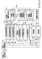
- Fig. 1 shows an information processing system to which an embodiment of a clock failure recovery system of the present invention is applied.
- the information processing system comprises processors 1 to 3, a clock oscillator 4, a clock distributor 5, clock failure detectors 61 to 63, an interrupt signal generator 7 as an interrupt generating means, a diagnosis processor 8, clock signal lines 101 to 103, 111 to 113, 121 to 123, 131 to 133, and 171, and signal lines 141 to 143, 151 to 154, and 161.
- the processor 1 is constituted by a plurality of packaging units 1-1 to 1-n. Each of the processors 2 and 3 is similarly constituted by a plurality of packaging units as in the processor 1.
- the clock oscillator 4 supplies a clock signal to the clock distributor 5 through the clock signal line 171.
- the clock distributor 5 independently distributes the clock signal through the clock signal lines 111 to 113, 121 to 123, and 131 to 133 in units of packaging units of the processors 1 to 3.
- the clock failure detectors 61 to 63 monitor the clock signals supplied from the clock distributor 5 to the packaging units of the processors 1 to 3 through the clock signal lines 101 to 103. When the detectors 61 to 63 detect an error, they inform it to the interrupt signal generator 7 through the signal lines 141 to 143.
- the interrupt signal generator 7 When the interrupt signal generator 7 is informed of an error from the clock failure detectors 61 to 63, it generates an interrupt signal, and outputs it to the diagnosis processor 8 through the signal line 161.
- the interrupt signal generator 7 has a status register 71 serving as an error signal holding means.
- the status register 71 holds data indicating a clock distribution system in which a failure occurs.
- the diagnosis processor 8 diagnoses the processors 1 to 3, and comprises an interrupt processing controller 81 and a failure recovery controller 82.
- the interrupt processing controller 81 recognizes that a clock error interrupt occurs when the interrupt signal input through the signal line 161 goes active, and informs it to the failure recovery controller 82.
- the failure recovery controller 82 performs failure recovery control of the processors 1 to 3, and can degrade the packaging units 1-1 to 1-n and can disconnect the processor 1 from the information processing system. The same operation as for the processor 1 is executed for the processors 2 and 3.
- the failure recovery controller 82 can perform read access of the status register 71 through the signal line 154, and logging of failure information.
- the clock failure detectors 61 to 63 detect it, and supply a message indicating it to the interrupt signal generator 7 through the signal lines 141 to 143.
- the interrupt signal generator 7 Upon reception of the message, the interrupt signal generator 7 generates an interrupt signal to interrupt the diagnosis processor 8 through the signal line 161.
- the interrupt processing controller 81 of the diagnosis processor 8 reads the status register 71 to recognize a processor in which a clock failure occurs. The controller 81 then instructs the failure recovery processor 82 to start a failure recovery program. The failure recovery controller 82 executes the failure recovery program, thereby performing clock failure recovery processing.
- Figs. 2 to 4 are flow charts showing the failure recovery programs.
- a failure recovery program (failure recovery A) shown in Fig. 2, a clock failure event is logged in step 90.
- the status register 71 is read to recognize a clock distribution system in which a clock failure occurs.
- the content of the status register 71 is logged.
- failure recovery of the entire information processing system is executed.
- failure recovery B failure recovery program shown in Fig. 3
- steps 90, 91, and 92 are executed similarly, failure recovery of only a processor in which a clock failure occurs is performed.
- a failure recovery program (failure recovery C) shown in Fig. 4, after steps 90, 91, and 92 are executed similarly, the interrupt from a processor in which a clock failure occurs is inhibited for a predetermined period of time.
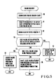
- step 92 The failure recovery processing operations described above are executed as one flow chart shown in Fig. 5.
- the same step numbers designate the same processing steps as in the flow charts in Figs. 2 to 4.
- Steps 90 to 92 are similarly executed for any failure recovery.
- step 110 the flow advances to step 110 to check if a failure occurs in a processor such as a system controller which influences the entire system. If YES in step 110, the flow advances to step 93 to execute the failure recovery A, so that failure recovery processing of the entire system is executed. If it is determined in step 110 that the failure occurs not in a processor such as a system controller which influences the entire system, the flow advances to step 111.
- step 111 it is checked whether or not the failure is a fatal one which is closed in one processor, in other words, whether or not the failure can be recovered as a fatal failure in the processor of interest. If YES in step 111, the failure recovery B is executed, so that failure recovery processing of a processor in which a clock failure occurs is executed. If it is determined in step 111 that the failure is not a fatal failure which is closed in one processor, e.g., an error of a display, the flow advances to step 95 to execute the failure recovery C. Thus, a failure interrupt from a processor in which a clock failure occurs is inhibited for a predetermined period of time. When such a failure frequently occurs, maintenance is performed in step 95 to cope with this failure.
- one of steps 93, 94, and 95 to be executed is determined depending on conditions of clock failures.
- the conditions of clock failures are that (1) a line is disconnected and no signal is input, (2) a clock cycle is disordered, (3) an object to be controlled falls outside a control range despite PLL control, and so on. If such a condition influences only one processor, processing in step 94 or 95 is executed, and when a condition is related to the entire system, processing in step 93 is executed.
- a clock error is detected by a clock failure detector, and a clock failure event and a location of the clock failure are logged by a failure recovery program, thus discriminating a clock failure or a logic portion failure. Therefore, a time required for analyzing a failure factor can be shortened.
Landscapes
- Engineering & Computer Science (AREA)
- Theoretical Computer Science (AREA)
- Quality & Reliability (AREA)
- Physics & Mathematics (AREA)
- General Engineering & Computer Science (AREA)
- General Physics & Mathematics (AREA)
- Health & Medical Sciences (AREA)
- Biomedical Technology (AREA)
- Debugging And Monitoring (AREA)
- Test And Diagnosis Of Digital Computers (AREA)
- Hardware Redundancy (AREA)
Claims (1)
- Taktausfallbeseitigungssystem in einem Informationsverarbeitungssystem mit mehreren Prozessoren (1 bis 3) und einem Diagnoseprozessor (8), das unabhängig die Ausfallbeseitigung für die mehreren Prozessoren (1 bis 3) ausführen kann, wobei das Taktausfallbeseitigungssystem dadurch gekennzeichnet ist, daß es aufweist:einen Taktverteiler (5) zum Erzeugen eines oder mehrerer in dem Informationsverarbeitungssystem verwendeter Taktsignale und Verteilen der Taktsignale zu den Prozessoren;Taktausfalldetektoren (61 bis 63) zum Überwachen der Taktsignalausgabe von dem Taktverteiler (5) und zum Erzeugen eines Fehlersignals in Einheiten von entsprechenden Prozessoren, wenn ein Fehler auftritt; undeine Unterbrechungserzeugungseinrichtung (7) mit einer Fehlersignalhalteeinrichtung (71) zum Halten des Fehlersignals zum Unterbrechen des Diagnoseprozessors (8) als Reaktion auf das Fehlersignal,wobei der Ausführungsbeginn eines Ausfallbeseitigungsprogramms zum Erkennen eines Prozessors, in dem ein Taktausfall auftritt, und Ausführen der Protokollierung eines Taktausfallereignisses und eines Taktausfallzustands in einem Unterbrechungsverarbeitungsprogramm des Diagnoseprozessors (8) gesteuert wird, das bei Unterbrechung gestartet wird.
Applications Claiming Priority (2)
| Application Number | Priority Date | Filing Date | Title |
|---|---|---|---|
| JP47540/89 | 1989-02-28 | ||
| JP1047540A JPH02226432A (ja) | 1989-02-28 | 1989-02-28 | クロック障害処理システム |
Publications (3)
| Publication Number | Publication Date |
|---|---|
| EP0385404A2 EP0385404A2 (de) | 1990-09-05 |
| EP0385404A3 EP0385404A3 (de) | 1992-06-17 |
| EP0385404B1 true EP0385404B1 (de) | 1996-06-19 |
Family
ID=12777974
Family Applications (1)
| Application Number | Title | Priority Date | Filing Date |
|---|---|---|---|
| EP19900103812 Expired - Lifetime EP0385404B1 (de) | 1989-02-28 | 1990-02-27 | Taktausfallbeseitigungssystem |
Country Status (3)
| Country | Link |
|---|---|
| EP (1) | EP0385404B1 (de) |
| JP (1) | JPH02226432A (de) |
| DE (1) | DE69027461T2 (de) |
Families Citing this family (5)
| Publication number | Priority date | Publication date | Assignee | Title |
|---|---|---|---|---|
| JPH09319456A (ja) * | 1996-06-03 | 1997-12-12 | Mitsubishi Electric Corp | 発振停止検出装置 |
| JP2000122749A (ja) | 1998-10-20 | 2000-04-28 | Mitsubishi Electric Corp | 発振停止検出装置 |
| JP3341712B2 (ja) * | 1999-06-08 | 2002-11-05 | 日本電気株式会社 | 交換装置の障害処理方式 |
| US6895525B1 (en) * | 1999-08-20 | 2005-05-17 | International Business Machines Corporation | Method and system for detecting phase-locked loop (PLL) clock synthesis faults |
| EP2193444A2 (de) * | 2007-09-03 | 2010-06-09 | Nxp B.V. | Taktüberwachungseinheit |
Family Cites Families (4)
| Publication number | Priority date | Publication date | Assignee | Title |
|---|---|---|---|---|
| JPS5966752A (ja) * | 1982-10-08 | 1984-04-16 | Nec Corp | 割込み方式 |
| US4651277A (en) * | 1983-09-16 | 1987-03-17 | Sanyo Electric Co., Ltd. | Control system for a magnetic disk drive unit |
| DE3335549A1 (de) * | 1983-09-29 | 1985-04-18 | Siemens AG, 1000 Berlin und 8000 München | Ueberwachungseinrichtung fuer eine datenverarbeitungsanlage |
| JPS6260019A (ja) * | 1985-09-10 | 1987-03-16 | Nec Corp | 情報処理装置 |
-
1989
- 1989-02-28 JP JP1047540A patent/JPH02226432A/ja active Pending
-
1990
- 1990-02-27 EP EP19900103812 patent/EP0385404B1/de not_active Expired - Lifetime
- 1990-02-27 DE DE1990627461 patent/DE69027461T2/de not_active Expired - Fee Related
Also Published As
| Publication number | Publication date |
|---|---|
| JPH02226432A (ja) | 1990-09-10 |
| EP0385404A2 (de) | 1990-09-05 |
| DE69027461T2 (de) | 1996-10-31 |
| DE69027461D1 (de) | 1996-07-25 |
| EP0385404A3 (de) | 1992-06-17 |
Similar Documents
| Publication | Publication Date | Title |
|---|---|---|
| US6012148A (en) | Programmable error detect/mask utilizing bus history stack | |
| US4996688A (en) | Fault capture/fault injection system | |
| US5630048A (en) | Diagnostic system for run-time monitoring of computer operations | |
| Carter et al. | Design of serviceability features for the IBM system/360 | |
| US20030084376A1 (en) | Software crash event analysis method and system | |
| US4916697A (en) | Apparatus for partitioned clock stopping in response to classified processor errors | |
| EP0385404B1 (de) | Taktausfallbeseitigungssystem | |
| JP2000187600A (ja) | ウオッチドッグタイマ方式 | |
| US4183462A (en) | Fault diagnosis apparatus and method for sequence control system | |
| KR100279204B1 (ko) | 자동제어시스템에서현장제어장치의콘트롤러이중화제어방법및그장치 | |
| US4785417A (en) | Electronic postage meter having an out of sequence checking arrangement | |
| JP3272195B2 (ja) | 冗長系切替監視制御装置 | |
| JPS6115239A (ja) | プロセツサ診断方式 | |
| JP3953467B2 (ja) | チップ中の欠陥を検出し報告するためのシステム | |
| EP0473806A1 (de) | Vorrichtung und Verfahren zur Fehlererkennung und -isolierung | |
| EP0342261B1 (de) | Einrichtung für die Fehlerkorrektur in einem selbstbewachten Datenverarbeitungssystem | |
| JPH0581080A (ja) | マイクロプロセツサの暴走監視装置 | |
| JPH1115661A (ja) | Cpuの自己診断方法 | |
| JP2767820B2 (ja) | 異常監視部の診断装置 | |
| JPH04283840A (ja) | 情報処理装置の診断方法 | |
| JP2006011991A (ja) | コンピュータ制御装置およびこのソフトウェア実行記録方式 | |
| JPS61245069A (ja) | 診断回路 | |
| JPH0764666A (ja) | クロック擾乱時の装置誤動作防止方式 | |
| JP2518652B2 (ja) | 多重系バス同期システムの割込み診断装置 | |
| JPS5983438A (ja) | プログラム異常検出方式 |
Legal Events
| Date | Code | Title | Description |
|---|---|---|---|
| PUAI | Public reference made under article 153(3) epc to a published international application that has entered the european phase |
Free format text: ORIGINAL CODE: 0009012 |
|
| 17P | Request for examination filed |
Effective date: 19900321 |
|
| AK | Designated contracting states |
Kind code of ref document: A2 Designated state(s): DE FR GB IT NL |
|
| PUAL | Search report despatched |
Free format text: ORIGINAL CODE: 0009013 |
|
| AK | Designated contracting states |
Kind code of ref document: A3 Designated state(s): DE FR GB IT NL |
|
| 17Q | First examination report despatched |
Effective date: 19931115 |
|
| GRAH | Despatch of communication of intention to grant a patent |
Free format text: ORIGINAL CODE: EPIDOS IGRA |
|
| GRAA | (expected) grant |
Free format text: ORIGINAL CODE: 0009210 |
|
| AK | Designated contracting states |
Kind code of ref document: B1 Designated state(s): DE FR GB IT NL |
|
| REF | Corresponds to: |
Ref document number: 69027461 Country of ref document: DE Date of ref document: 19960725 |
|
| RHK2 | Main classification (correction) |
Ipc: G06F 11/00 |
|
| ITF | It: translation for a ep patent filed | ||
| ET | Fr: translation filed | ||
| PLBE | No opposition filed within time limit |
Free format text: ORIGINAL CODE: 0009261 |
|
| STAA | Information on the status of an ep patent application or granted ep patent |
Free format text: STATUS: NO OPPOSITION FILED WITHIN TIME LIMIT |
|
| 26N | No opposition filed | ||
| PGFP | Annual fee paid to national office [announced via postgrant information from national office to epo] |
Ref country code: DE Payment date: 19991231 Year of fee payment: 11 |
|
| PGFP | Annual fee paid to national office [announced via postgrant information from national office to epo] |
Ref country code: FR Payment date: 20000210 Year of fee payment: 11 |
|
| PGFP | Annual fee paid to national office [announced via postgrant information from national office to epo] |
Ref country code: GB Payment date: 20000223 Year of fee payment: 11 |
|
| PGFP | Annual fee paid to national office [announced via postgrant information from national office to epo] |
Ref country code: NL Payment date: 20000228 Year of fee payment: 11 |
|
| PG25 | Lapsed in a contracting state [announced via postgrant information from national office to epo] |
Ref country code: GB Free format text: LAPSE BECAUSE OF NON-PAYMENT OF DUE FEES Effective date: 20010227 |
|
| PG25 | Lapsed in a contracting state [announced via postgrant information from national office to epo] |
Ref country code: NL Free format text: LAPSE BECAUSE OF NON-PAYMENT OF DUE FEES Effective date: 20010901 |
|
| GBPC | Gb: european patent ceased through non-payment of renewal fee |
Effective date: 20010227 |
|
| PG25 | Lapsed in a contracting state [announced via postgrant information from national office to epo] |
Ref country code: FR Free format text: LAPSE BECAUSE OF NON-PAYMENT OF DUE FEES Effective date: 20011031 |
|
| NLV4 | Nl: lapsed or anulled due to non-payment of the annual fee |
Effective date: 20010901 |
|
| REG | Reference to a national code |
Ref country code: FR Ref legal event code: ST |
|
| PG25 | Lapsed in a contracting state [announced via postgrant information from national office to epo] |
Ref country code: DE Free format text: LAPSE BECAUSE OF NON-PAYMENT OF DUE FEES Effective date: 20011201 |
|
| PG25 | Lapsed in a contracting state [announced via postgrant information from national office to epo] |
Ref country code: IT Free format text: LAPSE BECAUSE OF NON-PAYMENT OF DUE FEES;WARNING: LAPSES OF ITALIAN PATENTS WITH EFFECTIVE DATE BEFORE 2007 MAY HAVE OCCURRED AT ANY TIME BEFORE 2007. THE CORRECT EFFECTIVE DATE MAY BE DIFFERENT FROM THE ONE RECORDED. Effective date: 20050227 |