EP0377471A1 - Appareil numérique d'enregistrement et de reproduction d'un signal MUSE - Google Patents
Appareil numérique d'enregistrement et de reproduction d'un signal MUSE Download PDFInfo
- Publication number
- EP0377471A1 EP0377471A1 EP90100233A EP90100233A EP0377471A1 EP 0377471 A1 EP0377471 A1 EP 0377471A1 EP 90100233 A EP90100233 A EP 90100233A EP 90100233 A EP90100233 A EP 90100233A EP 0377471 A1 EP0377471 A1 EP 0377471A1
- Authority
- EP
- European Patent Office
- Prior art keywords
- signal
- data
- muse
- circuit
- bits
- Prior art date
- Legal status (The legal status is an assumption and is not a legal conclusion. Google has not performed a legal analysis and makes no representation as to the accuracy of the status listed.)
- Withdrawn
Links
Images


Classifications
-
- H—ELECTRICITY
- H04—ELECTRIC COMMUNICATION TECHNIQUE
- H04N—PICTORIAL COMMUNICATION, e.g. TELEVISION
- H04N9/00—Details of colour television systems
- H04N9/79—Processing of colour television signals in connection with recording
- H04N9/80—Transformation of the television signal for recording, e.g. modulation, frequency changing; Inverse transformation for playback
- H04N9/808—Transformation of the television signal for recording, e.g. modulation, frequency changing; Inverse transformation for playback involving pulse code modulation of the composite colour video-signal
-
- H—ELECTRICITY
- H04—ELECTRIC COMMUNICATION TECHNIQUE
- H04N—PICTORIAL COMMUNICATION, e.g. TELEVISION
- H04N5/00—Details of television systems
- H04N5/76—Television signal recording
- H04N5/91—Television signal processing therefor
- H04N5/92—Transformation of the television signal for recording, e.g. modulation, frequency changing; Inverse transformation for playback
- H04N5/923—Transformation of the television signal for recording, e.g. modulation, frequency changing; Inverse transformation for playback using preemphasis of the signal before modulation and deemphasis of the signal after demodulation
-
- H—ELECTRICITY
- H04—ELECTRIC COMMUNICATION TECHNIQUE
- H04N—PICTORIAL COMMUNICATION, e.g. TELEVISION
- H04N9/00—Details of colour television systems
- H04N9/79—Processing of colour television signals in connection with recording
- H04N9/797—Processing of colour television signals in connection with recording for recording the signal in a plurality of channels, the bandwidth of each channel being less than the bandwidth of the signal
-
- H—ELECTRICITY
- H04—ELECTRIC COMMUNICATION TECHNIQUE
- H04N—PICTORIAL COMMUNICATION, e.g. TELEVISION
- H04N9/00—Details of colour television systems
- H04N9/79—Processing of colour television signals in connection with recording
- H04N9/80—Transformation of the television signal for recording, e.g. modulation, frequency changing; Inverse transformation for playback
- H04N9/804—Transformation of the television signal for recording, e.g. modulation, frequency changing; Inverse transformation for playback involving pulse code modulation of the colour picture signal components
- H04N9/806—Transformation of the television signal for recording, e.g. modulation, frequency changing; Inverse transformation for playback involving pulse code modulation of the colour picture signal components with processing of the sound signal
- H04N9/8063—Transformation of the television signal for recording, e.g. modulation, frequency changing; Inverse transformation for playback involving pulse code modulation of the colour picture signal components with processing of the sound signal using time division multiplex of the PCM audio and PCM video signals
Definitions
- the present invention relates generally to digital recording and reproducing apparatuses, and, more particularly, digital recording and reproducing apparatuses for digitally recording on recording media such as a magnetic tape and an optical disc a high definition television (referred to as HDTV hereinafter) signal transmitted with a bandwidth being compressed in a MUSE (Multiple Sub-Nyquist Sampling Encoding) system and reproducing thus recorded signal.
- HDTV high definition television
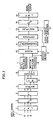
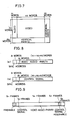
- Fig. 1 is a schematic block diagram showing a structure of a MUSE encoder for compressing a bandwidth of a HDTV signal according to the MUSE system and outputting the bandwidth-compressed HDTV signal as a MUSE signal.
- R, G and B of the HDTV signal each having a bandwidth of 30 MHz are supplied in parallel from, for example, a HDTV camera (not shown), and bands of which are limited by a low pass filter (LPF) 1 having a cut-off frequency of 21-22 MHz.
- LPF low pass filter
- the R, G and B of the HDTV signal are A/D converted by an A/D converter 2 at a sampling frequency of 48.6 MHz.
- the HDTV signal converted into a digital signal is subjected to a reverse processing with respect to the gamma characteristic of a camera in a gamma processing circuit 3, which is further applied to a matrix circuit 4.
- R, G, B of the HDTV signal are converted into a luminance (Y) signal and two color difference (C) signals, then bands of the two C signals are further limited by a LPF 5.
- the Y signal of 20 MHz and the two C signals each being of 7 MHz are applied to a TCI (Time Compressed Integration) encoder 6.
- the TCI encoder 6 puts the two C signals into a line sequence and compresses a time base thereof into 1/4, and thereafter which C signals are further time divisional multiplexed into the Y signal to output one series of the TCI video signals.
- a sub-sampling processing for compressing a bandwidth of the TCI signal is carried out. Described in more detail, a TCI signal of a still picture portion in a picture frame is subjected to a field off-set sub-sampling processing and a frame off-set sub-sampling processing by a sub-sampling circuit 7 for processing still picture and a TCI signal of a motion picture portion is subjected to a line off-set sub-sampling processing by a sub-sampling circuit 8 for processing motion picture.
- Such various sub-sampling processings are described in detail in the above described references (1), (2) and (3), which are not closely relevant to the present invention, and no further description will be given here.
- a motion detection circuit 9 detects the degree of a motion of picture in a motion picture portion, and a mixer 10 adjusts a mixing ratio of outputs of the still picture processing sub-sampling circuit 7 and the motion picture processing sub-sampling circuit 8 in response to the detected degree of the motion.
- the bandwidth of the TCI signal is compressed to 8.1 MHz.
- a gamma processing for a transmission path is performed by a gamma processing circuit 11 for the output of the mixer 10 and an emphasis processing is further performed by an emphasis circuit 12.
- a control signal (described later), a synchronizing signal and a digital audio signal from an audio encoder 14 (described later) are time divisional multiplexed into the thus processed video signal of 8.1 MHz by a multiple circuit 13.
- D/A converting thus obtained signal by a D/A converter 15 and limiting band of the D/A converted signal by a LPF 16 a transmission signal according to the MUSE system (referred to as MUSE signal hereinafter) can be obtained.
- the transmission according to the MUSE system is a transmission of analog sampled values and the sampling frequency thereof is 16.2 MHz.
- the above described MUSE signal transmission system having a bandwidth of 8.1 MHz fulfills a first standard of Nyquist at a transmission rate of 16.2 MHz. Accordingly, on a receiving side of the MUSE signal thus transmitted, the received MUSE signal can be completely re-sampled using a clock which is in synchronization with the train of the sampled values and has a clock rate twice the Nyquist frequency (8.1 MHz), that is, a clock rate of 16.2 MHz.
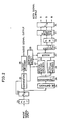
- Fig. 2 is a schematic block diagram showing a structure of a MUSE decoder for restoring a received MUSE signal to a HDTV signal.
- the received MUSE signal has a bandwidth limited by a LPF 21, which is further A/D converted by an A/D converter 22.
- An output of the A/D converter 22 is subjected to the de-emphasis processing by a de-emphasis circuit 24, which is further subjected to a reverse processing with respect to the gamma characteristic of a transmission path by a gamma processing circuit 26.
- the output of the A/D converter 22 is also applied to a separation circuit 23, thereby the audio signal which has been time divisional multiplexed into the received MUSE signal is extracted to be applied to an audio encoder 25.
- a signal interpolation processing is performed to an output of the gamma processing circuit 26. More specifically, an intra-field interpolation processing is performed by a motion picture processing circuit 27 for a signal of a motion picture portion in the picture frame and inter-frame and inter-field interpolation processings are performed by a still picture processing circuit 28 for a signal of a still picture portion.
- a motion picture processing circuit 27 for a signal of a motion picture portion in the picture frame
- inter-frame and inter-field interpolation processings are performed by a still picture processing circuit 28 for a signal of a still picture portion.
- a motion detection circuit 29 detects the degree of a motion of picture in the motion picture portion and a mixer 30 adjusts a mixing ratio of outputs of the circuits 27 and 28 in response to the detected degree of motion.
- the TCI video signal thus restored are supplied to a TCI decoder 31 to be TCI decoded into the original Y signal and the two C signals.
- the bandwidths of the two C signals are limited by a LPF 32.
- the Y signal and the C signals are subjected to a reverse matrix processing by a reverse matrix circuit 33, so that the original R, G, and B signals are obtained.
- Outputs of the reverse matrix circuit 33 is D/A converted by a D/A converter 34 and restored as the HDTV signals of R, G, B.
- Fig. 3 is a diagram schematically showing a signal form of such a MUSE signal as described above.
- the sampling frequency of the MUSE signal is 16.2 MHz
- the signal form of Fig. 3 is numbered at sampling intervals of 16.2 MHz.
- 1H period that is, one scanning line (referred to as a line hereinafter) comprises 480 sampling points, and 1 frame (two fields) is comprised of 1125 lines.
- a horizontal synchronizing signal HD
- C signal a C signal
- Y signal a control signal
- guard portion for preventing signal interference between the Y and C, respectively.
- the C signal is included in the signal regions having the line numbers 43-558 and 605-1120 wherein R-Y signal and B-Y signal are line-sequentially multiplexed in the odd-numbered lines and the even-numbered lines respectively.
- the Y signal is included in the signal regions having the line numbers 47-562 and 609-1124.
- the control signal is included in the signal regions having the line numbers 559-563 and 1121-1125.
- Fig. 4 shows the contents of the control signal including sub-sampling phase, motion vector amount and codes for discriminating between an FM modulation and an AM modulation in a modulation system in transmitting MUSE signals. The contents of such a control signal is described in detail in the above described references (1), (2) and (3), and no further description will be given here.
- the rest of the regions in the signal form of Fig. 3 correspond to a vertical blanking period, wherein the regions having the line numbers 1 and 2 each includes VIT signals used for equalization of a transmission path and the regions having the line numbers 563 and 1125 each includes clamp level signals used for defining an neutral level of the C signal and for AFC.
- the signal regions having the line numbers 3-46 and 565-608 each includes audio data and other additional information. The additional information is non-specified, arbitrary data.
- the regions having the line numbers 43-46 and 605-608 each includes a part of the C signal region.
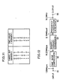
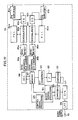
- Fig. 5 is a schematic block diagram showing a structure of such a digital VTR.
- a MUSE signal supplied to an input terminal 51 in recording from, for example, the MUSE encoder of Fig. 1 is converted into a digital MUSE signal by a digital recording circuit 52, and thereafter subjected to processing such as time base compression and addition of error correcting codes, and further modulated.
- the modulated digital MUSE signal is supplied to a rotary magnetic head 57 through a switching circuit 55 and a rotary transformer 56 and recorded on a magnetic tape 58.
- the digital MUSE signal recorded on the magnetic tape 58 is read out by the rotary magnetic head 57 and applied to a digital reproducing circuit 54 through the rotary transformer 56 and the switching circuit 55.
- the digital reproducing circuit 54 demodulates the digital signal and subjects the demodulated signal to such processings as a time base correction and code error correction, thereby outputting the demodulated digital signal as the MUSE signal.
- the outputted MUSE signal is restored to the original HDTV signal by, for example, the MUSE decoder of Fig. 2 and supplied to a HDTV monitor TV or the like.
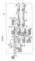
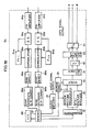
- Fig. 6 is a block diagram showing in detail the digital recording circuit 52 shown in Fig. 5.
- the MUSE signal inputted to the input terminal 51 has a bandwidth limited by a Nyquist filter 61 which is the LPF of 8.1 MHz, which is converted into a digital signal by an A/D converter 63 thereafter.
- the MUSE signal is transmitted in the form of the sampled values as described above and the sampled values should be reproduced correctly.
- a re-sampling clock of 16.2 MHz in synchronization with the MUSE signal is reproduced by a PLL circuit 62, and A/D conversion is performed based on this clock.
- the digital MUSE signal outputted from the A/D converter 63 is separated into a video signal, a control signal and other signal such as an audio signal by a separation circuit 64, and each of which is stored in a memory 66. On this occasion, predetermined processings are performed to the audio signal and the control signal by an audio signal processing circuit 65 and a control signal processing circuit 67, respectively.
- the parity generating circuit 68 generates a vertical parity and a horizontal parity so as to constitute a correction block shown in Fig. 7 and store the same in the memory 66.
- One unit of the correction block shown in Fig. 7 comprises an audio signal of n1 words, a video signal of n2 words and a horizontal parity of n3 words with respect to a horizontal direction and an audio or video signal of m1 words and a vertical parity of m2 words with respect to a vertical direction.
- n1, n2, n3, m1 and m2 are set to 2, 120, 5, 86 and 4, respectively.
- k blocks of the correction blocks of Fig. 7 constitute one scan track (referred simply to as a track hereinafter) and L scans of the tracks constitute the data of one field.
- one field is comprised of 6 tracks and each track is comprised of 4 correction blocks.
- the correction block of Fig. 7 is the data corresponding to 1/24 field.
- the audio data, the video data, the control signal and the parity are sequentially read out from the memory 66 and distributed to the respective channels so as to be applied to data frame composing circuits 72a and 72b.
- a plurality of systems (for example two systems) of circuits are provided in the subsequent stages of the data frame composing circuits because the channel distribution recording system is adopted.
- the synchronizing signal and the address signal are supplied from a synchronizing signal generating circuit 69 and an address signal generating circuit 70 respectively to both of the data frame composing circuits 72a and 72b.
- the data frame composing circuits 72a and 72b compose one unit of data frame including the synchronization data of l1 words, the address data of l2 word, the data of (n1 + n2 + n3) words comprising the audio, the video and the parity, in this sequence in accordance with the supplied data as shown in Fig. 8 (a) and output the same. More specifically, the data frame shown in Fig. 8 (a) corresponds to one horizontal line of data in the correction block of Fig. 7, and the address data of l2 words includes the data comprising the number for identifying the corresponding data frame, the numbers of the block and the track including the corresponding data frame and the numbers of the field and the frame (picture).
- the data frame composing circuits 72a and 72 sequentially feed the above described data frames corresponding to respective lines of the correction block and apply the same to the data composing circuits 73a and 73b.
- the data frame composing circuits 72a and 72b in response to the control signal read out from the memory 66, the synchronizing signal and the address signal from the synchronizing signal generating circuit 69 and the address signal generating circuit 72 respectively, compose one unit of the data frame including the synchronization data of l1 words, the address data of l2 words and the control signal of (n1+n2+n2) words in this sequence as shown in Fig. 8 (b) and output the same to be applied to the data composing circuits 73a and 73b, respectively.
- a preamble signal and a postamble signal are supplied from a preamble/postamble signal generating circuit 71 to the data composing circuits 73a and 73b, respectively.
- the data composing circuits 73a and 73b compose signals of one track having an arrangement as shown in Fig. 9, based on the various data received from the data frame composing circuits 72a and 72b and the preamble/postamble signal generating circuit 71.
- the signal of one track shown in Fig. 9 comprises a preamble signal of S1 frames, a control signal of S2 frames, data of S4 frames comprising audio, video and parity, a control signal of S2 frames and a postamble signal of S3 frames.
- the preamble portion and the postamble portion are provided at the opposite edges of the recording track as shown in Fig. 9 for a margin in switching the head, that is, a leading-in time period for clock reproduction and the absorption of a rotary jitter of a cylinder and the like, in the digital VTR for recording using a rotary head.
- the preamble signal and the postamble signal recorded in these portions are usually signals having a fixed frequency corresponding to the maximum value or one fraction of integral number of the recording frequency of the signal to be digitally recorded.
- the signals each composed one scan track basis are modulated in digital modulation circuits 74a and 74b, and thereafter amplified by recording amplifying circuits 75a and 75b. Then, the signals of two channels outputted from the recording amplifying circuits 75a and 75b are switched into two systems by the switching circuit 55 of Fig. 5 in accordance with a rotating phase of the rotary head, and fed to the rotary magnetic heads 57 through the rotary transformer 56, which are further recorded on the magnetic tape 58.
- Fig. 10 is a block diagram showing in detail the digital reproduction circuit 54 shown in Fig. 5.
- the signal recorded on the magnetic tape 58 is read out by the rotary magnetic heads 57 and applied to reproduction amplifying circuits 81a and 81b in the digital reproduction circuit 54 through the rotary transformer 56 and the switching circuit 55.
- the signals amplified by the reproduction amplifying circuits 81 and 81b are waveform shaped by waveform equalizing circuits 82a and 82b so as to compensate the characteristics lost in the magnetic recording and reproducing system and applied to demodulation circuits 83a and 83b and PLL circuits 84a and 84b.
- the PLL circuits 84a and 84b generate clocks based on the applied reproduced signal, apply the same to the demodulation circuits 83a and 83b respectively, so that demodulation circuits 83a and 83b demodulate the outputs of the waveform equalizing circuits 82a and 82b to the original data signals in response thereto.
- the demodulated digital signals are applied to the synchronization detecting circuits 85a and 85b to detect the synchronization data.
- Synchronization separating and serial/parallel converting circuits 86a and 86b separate the data from the demodulated digital signals to carry out the serial/parallel conversion based on the detected synchronizing signals and write the separated data into the memory 87 on a word basis.
- the data written in the memory 87 is sequentially read out to the error correction circuit (ECC) 88, subjected to a correction processing and an interpolation processing, and written into the memory 87 again.
- ECC error correction circuit
- the data stored in the memory 87 is read out to a MUSE decoder interface circuit 89 to be restored to the original MUSE signal form, and thereafter outputted from the output terminal 53.
- the form of the MUSE signal outputted from the output terminal 53 namely, whether it is outputted as an analog signal or a digital signal, or how a video signal and an audio signal are separated is determined in accordance with the specification of the MUSE decoder (for example, the decoder shown in Fig. 2) to be connected in the subsequent stage of the terminal 53.
- the audio data and other additional information included in the signal regions indicated as the line numbers 3-46 and 565-608 before they are multiplexed into a MUSE signal are originally binary signals comprising "0" or "1" to be transmitted in serial at a bit rate of 1.35 Mbps. Since the audio data as the binary signal is transmitted in the above described MUSE signal transmission system having a Nyquist frequency of 8.1 MHz, it is subjected to a processing such as a time base compression by the audio encoder 14, and then time divisional multiplexed into the vertical blanking portion of the MUSE signal shown in Fig. 3.
- Fig. 12 is a block diagram showing a circuit structure for the audio data processing included in the audio encoder 14 and an operational principle thereof is disclosed in detail in Japanese Patent Laying-Open No. 62-172874.
- the audio data having the bit rate of 1.35 Mbps inputted from an input terminal 91 has a time base compressed by a time base compression circuit 92, resulting in a signal having the bit rate of 18.225 Mbps.
- the binary signal of 18.225 Mbps is converted into a ternary signal comprising "0", "1" or "2" by a binary/ternary converting circuit 93, based on a binary/ternary conversion table shown in Fig. 11 and outputted at the frequency of 12.15 MHz.
- the ternary signal is frequency-converted by a frequency conversion circuit 94 and outputted from the terminal 95 as a signal having a frequency of 16.2 MHz.
- a sampling frequency of the audio data becomes the same as that of the MUSE video signal, thereby enabling the transmission in the transmission system of the Nyquist frequency of 8.1 MHz.
- the audio data is further supplied to a multiplex circuit 13 constituting the MUSE encoder shown in Fig. 1 to be time divisional multiplexed into the MUSE video signal.
- an audio data multiplexed into a MUSE video signal is basically a digital signal of a ternary value and different from an Y signal and a C signal which are originally analog signals.
- the following problems occur when the bit number, that is, a resolution, in quantizing such a MUSE signal in the recording circuit of the digital VTR (Fig. 6) is set on the basis of the resolution of the analog value (for example eight bits) to quantize the audio data which is the ternary signal.
- the audio data in the form of the ternary signal occupies about 8% of the data amount of the entire MUSE signal, so that when the audio data is quantized by the same resolution as that of the video signal portion to be digitally recorded, instead of one bit, as many as eight bits are required as required for the quantization of the analog signal.
- a recording rate in digital recording is increased, a recording wavelength is shortened, which causes the error in the recorded data to be increased.
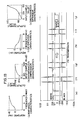
- Figs. 13 (a)-(j) are graphs and waveform diagrams for explaining these various processings.
- the video signal which changes white ⁇ black ⁇ white as shown in Fig. 13 (e) is subjected to a processing of an emphasis characteristics shown in Fig. 13 (a) by the emphasis circuit 12, so that the edge portions of the video signal are emphasized as shown in Fig. 13 (f).
- the signal is subjected to a processing of instantaneous amplitude compression characteristic of Fig. 13 (b) by the emphasis circuit 12, so that the emphasis of the edge portions is suppressed as shown in Fig. 13 (g).
- the signal thus processed is FM transmitted, and after the signal is received (Fig.
- the video signal in the MUSE signal is subjected to the emphasis processing.
- the video signal to be recorded (Fig. 13 (h)) should be quantized with ten bits of fineness (- 512 to 511) to be digitally recorded.
- N is a positive integer
- digital recording should be performed with (N + 2) numbers of quantization bits.
- An object of the present invention is to prevent generation of errors in the recorded data in a digital recording apparatus for the MUSE signal.
- Another object of the present invention is to reduce a bit rate for the recorded data in a digital recording apparatus for the MUSE signal without enlarging a circuit structure.
- the present invention is a digital recording apparatus for digitally recording a MUSE signal comprising a plurality of kinds of data on a recording medium. At least part of the plurality of data is coded or modulated using the number of bits larger than that of the original HDTV signal.
- the data having the increased number of bits is subjected to a processing for reducing the bit number, and which is recorded on the recording medium thereafter.
- At least an audio signal in the MUSE signal is converted into a ternary signal with an increased bit number, and this audio signal is converted into the original binary signal in the time of digital recording.
- At least a video signal in the MUSE signal is subjected to the emphasis processing with the increased number of bits, and in the time of the digital recording, this audio signal is subjected to the de-emphasis processing.
- a principal advantage of the present invention is that the amount of data information to be digitally recorded can be drastically compressed to reduce a recording bit rate for the entire MUSE signal.
- Fig. 14 is a block diagram showing a digital recording circuit of a digital VTR according to a first embodiment of the present invention.
- a digital recording circuit 52 receives a MUSE signal from an input terminal 51, modulates the same into a recording signal of two channels and supplies the modulated signal to a switching circuit 55.
- a digital recording and reproducing system (55-58) and a digital reproducing circuit 54 of the digital VTR according to this embodiment are the same as those of the prior art shown in Fig. 5 and Fig. 10, and no farther description will be given.
- the digital recording circuit 52 shown in Fig. 14 is the same as the conventional digital recording circuit 52 shown in Fig. 6 except for the following points, so that no farther description will be repeated for the parts which are the same in both circuit. Namely, in place of the audio processing circuit 65 of Fig. 6, a frequency converting circuit 101, a ternary discrimination circuit 102 and a two-bit indicating circuit 102 are provided.
- the audio data (including the additional information) is separated by a separation circuit 64 from the MUSE signal A/D converted by an A/D converter 63 and the separated audio data is applied to the frequency converting circuit 101.
- the frequency converting circuit 101 converts the audio data having a sampling frequency of 16.2 MHz into a ternary signal having a sampling frequency of 12.15 MHz.
- the ternary signal is applied to the ternary discrimination circuit 102, which circuit discriminates a tri-state of the ternary signal at one sampling point, that is, which level the signal has among 0, 1 and 2 and applies one discrimination result to the two-bit indicating circuit 103.
- the two-bit indicating circuit 103 indicates the obtained result of the ternary discrimination as a digital signal of two bits. More specifically, while the MUSE signal resampled in the A/D converter 63 includes eight bits at one sampling point, the value indicated by a ternary signal at the one sampling point, that is, 0, 1 or 2 can be indicated by a binary signal of two bits. Such a digital signal of two bits is stored in a memory 66. That is, the number of bits required for the audio data at one sampling point can be reduced from eight bits to two bits, thereby drastically reducing a bit rate for a signal to be digitally recorded on a magnetic tape.
- Fig. 15 is a block diagram showing a digital recording circuit of a digital VTR according to a second embodiment of the present invention.
- the digital recording circuit 52 shown in Fig. 15 is the same as the first embodiment shown in Fig. 4 except for the following points.
- a ternary/binary converting circuit 104 is provided in place of the two-bit indicating circuit 103 of Fig. 14. More specifically, the ternary discrimination circuit 102 applies to the ternary/binary converting circuit 104 a tri-state of the ternary signal at each sampling point applied from the frequency converting circuit 101, that is, a result of discrimination among the signal levels of 0, 1 and 2.
- the ternary/binary converting circuit 104 upon receiving two discrimination results in succession, converts the same into a digital (binary) signal of three bits based on a conversion table shown in Fig. 11. Namely, while the MUSE signal resampled in the A/D converter 63 includes a total of 16 bits at two sampling points, these two sampling points almost correspond to two ternary signals and the values indicated by the two ternary signals can be indicated by binary signals having three bits. Then, such a digital signal having three bits is stored in the memory 66. That is, the number of bits required for the audio data at the two sampling points can be reduced from 16 bits to 3 bits by the circuit of Fig. 15, thereby reducing a bit rate for a signal to be digitally recorded on the magnetic tape.
- Both of the two-bit indicating circuit 103 shown in Fig. 14 and the ternary/binary converting circuit 104 shown in Fig. 15 may be provided to receive an output of the ternary discrimination circuit 102, such that the outputs of the circuits 103 and 104 are simultaneously written into the memory 66 as the audio data, or selected one of the outputs of the circuit 103 and 104 is written into the memory 66.
- the resampling frequency of the audio data is converted from 16.2 MHz to 12.15 MHz by the frequency converting circuit 101
- the resampling frequency may be set to 48.6 MHz which is a least common multiple of 16.2 MHz and 12.15 MHz to thin out down to one-fourth the sampling of the audio data A/D converted at this frequency at an appropriate timing and an equal interval, thereby generating the audio data of 12.5 MHz to be applied to the ternary discrimination circuit 102.
- the information amount of the audio data to be digitally recorded can be drastically compressed to reduce a recording rate for the entire MUSE signal.
- reduction of a recording wavelength can be prevented and occurrence of errors in the recording data can be suppressed without enlarging a size for a VTR system.
- Figs. 16 and 17 are block diagrams showing a digital recording circuit and a digital reproducing circuit respectively of a digital VTR according to a third embodiment of the present invention respectively.
- the digital recording circuit 52 shown in Fig. 16 in the same manner as the prior art shown in Fig. 5, receives a MUSE signal through the input terminal 51, modulates the same into a recording signal of two channels and supplies the modulated signal to the recording circuit 55 (Fig. 5).
- a magnetic recording and reproducing system (55-58) of the digital VTR according to this embodiment is the same as that of the prior art shown in Fig. 5.
- the reproduced signal from the switching circuit 55 of Fig. 5 is applied to the digital reproducing circuit 54 of Fig. 17, which circuit demodulates the same to be restored as a MUSE signal and outputs thus restored signal through the output terminal 53.
- the digital recording circuit 52 shown in Fig. 16 is the same as the conventional digital recording circuit 52 shown in Fig. 6 except for the following points. More specifically, a de-emphasis circuit 111, a reverse gamma correction circuit 112 for transmission path and a bit converting circuit 113 are interposed in a video signal path between the separation circuit 64 and the memory 66.
- the video data is separated by the separation circuit 64 from the MUSE signal A/D converted by the A/D converter 63 and applied to the de-emphasis circuit 111.
- the separated video data is a signal of ten bits of fineness having a waveform shown in Fig. 13 (h).
- the de-emphasis circuit 111 has the de-emphasis characteristic and instantaneous amplitude expansion characteristic shown in Fig. 13 (c) and (d) respectively, subjects the video signal separated from the digital MUSE signal by the separation circuit 64, to the de-emphasis processing and the instantaneous amplitude expansion processing, thereby applying the video signal having the waveform of Fig. 13 (j) to the reverse gamma correction circuit 112 for transmission path.
- the video data reverse-gamma corrected by the reverse gamma correction circuit 112 is further applied to the bit number converting circuit 113, wherein the number of bits thereof is converted from ten bits to eight bits. As shown in Fig.
- the de-emphasized video signal herein is in the range of a level width of - 128 to 127, so that conversion from ten bits to eight bits can be implemented by simply taking out a most significant code bit and following less significant seven bits, that is, most significant eight bits. Meanwhile, it may be constituted such that the above described processings such as the ternary discrimination of the audio data shown in the above described first and the second embodiments is performed in the audio signal processing circuit 65.
- the video signal converted to have eight bits of fineness (Fig. 13 (j)) is recorded on the magnetic tape. Then, the video data of eight bits read out from the magnetic tape in the time of reproduction is supplied to the digital reproducing circuit 54 shown in Fig. 17.
- the digital reproducing circuit 54 shown in Fig. 17 is the same as the conventional digital reproducing circuit 54 shown in Fig. 10 except for the following points. Namely, in place of the MUSE interface circuit 89 of Fig. 10, a bit number converting circuit 121, a gamma correction circuit 122 for transmission path, an emphasis circuit 123, an audio signal processing circuit 124, a control signal processing circuit 125, a composing circuit 126, a D/A converter 127 and an LPF 128 are provided.
- each of video, audio and control signals each subjected to error correction and the like by the error correction circuit 88 is read out from the memory 87.
- the video data having eight bits of fineness read from the memory 87 is converted into the data of ten bits of fineness by the bit number converting circuit 121, which is further applied to the gamma correction circuit 122 for transmission path.
- An output of the gamma correction circuit 122 is applied to the emphasis circuit 123 having the emphasis characteristic and instantaneous amplitude compression characteristic shown in Figs. 13 (a) and (b) respectively, wherein the output is subjected to the emphasis and instantaneous amplitude compression processings.
- each signal is composed in the composing circuit 126 to constitute a MUSE signal of the signal form of Fig. 3.
- the MUSE signal thus obtained is D/A converted by the D/A converter 127, and thereafter bandwidth limited in the LPF 128 to be supplied as the MUSE signal through the output terminal 53.
- the recording rate for the entire MUSE signal can be reduced to prevent the generation of the errors in the recorded data.
- the digital VTR in accordance with the third embodiment as shown in Fig. 16 and Fig. 17 is a VTR in which the MUSE signal is recorded and reproduced. Accordingly, in order to display the image produced by the video data reproduced by the VTR of this embodiment on a monitor picture frame, an output MUSE signal of the VTR should be supplied to a HDTV monitor after once being converted into a HDTV signal using the MUSE decoder, for example, shown in Fig. 2. In such a case, the de-emphasis processing is performed once again by the de-emphasis circuit (for example the circuit 24 of Fig. 2) in the MUSE decoder.
- the de-emphasis circuit for example the circuit 24 of Fig. 2
- Fig. 18 is a schematic block diagram showing an apparatus in accordance with the fourth embodiment of the present invention which incorporates the MUSE decoder into the digital reproducing circuit of such a digital VTR. More specifically, in the fourth embodiment shown in Fig. 18, the output of the memory 87 in the digital reproducing circuit 54 of Fig. 17 is supplied directly to the respective circuits 26, 27 and 29 of Fig. 2 as the outputs of the separation circuit 23 and the emphasis circuit 24 of the MUSE decoder of Fig. 2, which makes the respective circuit 121-128 of Fig. 17 and the respective circuits 21-24 of Fig. 2 unnecessary.
- the digital reproducing circuit 54 of the digital VTR in accordance with the third embodiment shown in Fig. 17 is structured as to output a MUSE signal subjected to the emphasis processing as an reproduced output of the VTR.
- the emphasis circuit 123 having the same structure as that of the emphasis circuit 12 provided in the MUSE encoder of Fig. 1 is required in the digital reproducing circuit 54, causing a circuit structure of the digital reproducing circuit to be larger.
- Fig. 19 and Fig. 20 are block diagrams showing a digital recording circuit and a digital reproducing circuit of the digital VTR according to the fifth embodiment in which the above described problems are solved, respectively.
- the digital recording circuit 52 shown in Fig. 19 is the same as the conventional digital recording circuit 52 shown in Fig. 16 except for the following points. More specifically, the digital recording circuit 52 shown in Fig. 19 receives the MUSE signal through the input terminal 51 from, for example, the MUSE encoder shown in Fig. 1.
- the received MUSE signal includes the control signal having the contents shown in Fig. 4 with the value of the 20th bit thereof indicating whether the MUSE video signal is subjected to the emphasis processing or not.
- a value of the 20th bit of the control signal is "0", while in case that the MUSE video signal is not subjected to the emphasis processing and is AM modulated, the value is "1".
- the control signal processing circuit discriminates the value of the 20th bit to control the signal selecting circuit 131 in accordance with the discrimination result.
- the signal selecting circuit 131 selects an output of the emphasis circuit 111 and writes the same into the memory 66 when the 20th bit of the control signal is "0", that is, it is subjected to the emphasis processing, and writes an output of the separation circuit 64 directly into the memory 66 when the 20th bit of the control signal is "1", that is, it is not subjected to the emphasis processing.
- the signal selecting circuit 131 contains the reverse gamma correction circuit 112 and the bit number converting circuit 113 of Fig. 16 to subject the selected video data to the above described reverse gamma correction and the bit number converting processings. Therefore, according to the digital recording circuit of Fig. 19, the video data is always outputted which is not subjected to the emphasis processing.
- the digital reproducing circuit 54 of Fig. 20 does not include the emphasis circuit 123 shown in Fig. 17, therefore the digital reproducing circuit 54 outputs the MUSE signal not subjected to the emphasis processing from the output terminal 53.
- the control signal processing circuit 125 forcibly sets the 20th bit of the control signal of the outputted MUSE signal to "1" showing the AM modulation.
- the MUSE decoder of the monitor TV receiving the outputted MUSE signal processes the video signal without subjecting the same to the de-emphasis processing.
- Such a forced setting of the control signal may be performed by the control signal processing circuit 67 of the digital recording circuit 52 before the recording on the magnetic tape.
- the reproduced MUSE signal can be forcibly set to indicate the AM mode wherein no emphasis processing is performed, so that the digital reproducing circuit can do without an emphasis circuit.
- the video data is subjected to the de-emphasis processing after being A/D converted in the digital recording circuit
- the analog video signal may be subjected to the de-emphasis processing first, and A/D converted thereafter.
- an amplitude of the A/D converted signal becomes smaller, so that the number of bits of the information to be digitally recorded can be further compressed.
- first to fifth embodiments are examples in which the present invention is applied to the digital VTR as the magnetic recording and reproducing apparatus, the present invention is not limited to such a digital VTR and it may be applied to any kind of recording apparatuses (for example optical disk recording apparatus) for digitally recording a MUSE signal.
- recording apparatuses for example optical disk recording apparatus
- the present invention is not limited to such a MUSE signal and it may be applied to a HDTV signal transmitted in any kind of transmission systems.
Landscapes
- Engineering & Computer Science (AREA)
- Multimedia (AREA)
- Signal Processing (AREA)
- Television Signal Processing For Recording (AREA)
- Television Systems (AREA)
Applications Claiming Priority (4)
| Application Number | Priority Date | Filing Date | Title |
|---|---|---|---|
| JP1595/89 | 1989-01-06 | ||
| JP1001595A JPH02182089A (ja) | 1989-01-06 | 1989-01-06 | Muse信号の記録装置 |
| JP3094/89 | 1989-01-10 | ||
| JP1003094A JP2815882B2 (ja) | 1989-01-10 | 1989-01-10 | 映像信号のデジタル記録再生装置 |
Publications (1)
| Publication Number | Publication Date |
|---|---|
| EP0377471A1 true EP0377471A1 (fr) | 1990-07-11 |
Family
ID=26334848
Family Applications (1)
| Application Number | Title | Priority Date | Filing Date |
|---|---|---|---|
| EP90100233A Withdrawn EP0377471A1 (fr) | 1989-01-06 | 1990-01-05 | Appareil numérique d'enregistrement et de reproduction d'un signal MUSE |
Country Status (3)
| Country | Link |
|---|---|
| US (1) | US5124812A (fr) |
| EP (1) | EP0377471A1 (fr) |
| CA (1) | CA2007278A1 (fr) |
Cited By (2)
| Publication number | Priority date | Publication date | Assignee | Title |
|---|---|---|---|---|
| EP0502708A1 (fr) * | 1991-03-04 | 1992-09-09 | Sharp Kabushiki Kaisha | Appareil d'enregistrement/reproduction numérique pour un signal MUSE et procédé d'utilisation de l'appareil |
| EP0578509A1 (fr) * | 1992-07-10 | 1994-01-12 | Sony Corporation | Appareil de reproduction d'un signal d'information audiovisuelle |
Families Citing this family (4)
| Publication number | Priority date | Publication date | Assignee | Title |
|---|---|---|---|---|
| US6002536A (en) * | 1990-07-06 | 1999-12-14 | Hitachi Ltd. | Digital transmission signal processing system and recording/reproducing system |
| JP2947978B2 (ja) * | 1991-06-21 | 1999-09-13 | 株式会社日立製作所 | 音声信号記録再生装置 |
| JP3623056B2 (ja) * | 1996-09-10 | 2005-02-23 | ソニー株式会社 | 動画像圧縮装置 |
| KR100460774B1 (ko) * | 2002-10-10 | 2004-12-09 | 매그나칩 반도체 유한회사 | 어드레스 서브샘플링 장치 및 그 방법과 이미지센서 및이미지센서의 어드레스 서브샘플링 방법 |
Citations (4)
| Publication number | Priority date | Publication date | Assignee | Title |
|---|---|---|---|---|
| US4551773A (en) * | 1982-07-16 | 1985-11-05 | Sperry Corporation | Encoding and decoding apparatus and method utilizing hierarchical code substitution |
| US4692801A (en) * | 1985-05-20 | 1987-09-08 | Nippon Hoso Kyokai | Bandwidth compressed transmission system |
| GB2215555A (en) * | 1988-02-05 | 1989-09-20 | Hitachi Ltd | Image data transfer method and apparatus therefor |
| EP0337650A1 (fr) * | 1988-04-07 | 1989-10-18 | Sony Corporation | Appareil magnétique d'enregistrement et de reproduction |
Family Cites Families (2)
| Publication number | Priority date | Publication date | Assignee | Title |
|---|---|---|---|---|
| JP2702108B2 (ja) * | 1985-04-15 | 1998-01-21 | 三菱電機株式会社 | Muse方式映像記録再生装置,muse方式映像受信記録再生装置,museデコーダ及びディジタルmuse信号記録再生装置 |
| GB8729878D0 (en) * | 1987-12-22 | 1988-02-03 | Philips Electronic Associated | Processing sub-sampled signals |
-
1990
- 1990-01-03 US US07/460,578 patent/US5124812A/en not_active Expired - Lifetime
- 1990-01-05 CA CA002007278A patent/CA2007278A1/fr not_active Abandoned
- 1990-01-05 EP EP90100233A patent/EP0377471A1/fr not_active Withdrawn
Patent Citations (4)
| Publication number | Priority date | Publication date | Assignee | Title |
|---|---|---|---|---|
| US4551773A (en) * | 1982-07-16 | 1985-11-05 | Sperry Corporation | Encoding and decoding apparatus and method utilizing hierarchical code substitution |
| US4692801A (en) * | 1985-05-20 | 1987-09-08 | Nippon Hoso Kyokai | Bandwidth compressed transmission system |
| GB2215555A (en) * | 1988-02-05 | 1989-09-20 | Hitachi Ltd | Image data transfer method and apparatus therefor |
| EP0337650A1 (fr) * | 1988-04-07 | 1989-10-18 | Sony Corporation | Appareil magnétique d'enregistrement et de reproduction |
Cited By (4)
| Publication number | Priority date | Publication date | Assignee | Title |
|---|---|---|---|---|
| EP0502708A1 (fr) * | 1991-03-04 | 1992-09-09 | Sharp Kabushiki Kaisha | Appareil d'enregistrement/reproduction numérique pour un signal MUSE et procédé d'utilisation de l'appareil |
| US5220435A (en) * | 1991-03-04 | 1993-06-15 | Sharp Kabushiki Kaisha | Muse signal digital recording/reproducing apparatus and operating method thereof |
| EP0578509A1 (fr) * | 1992-07-10 | 1994-01-12 | Sony Corporation | Appareil de reproduction d'un signal d'information audiovisuelle |
| US5400305A (en) * | 1992-07-10 | 1995-03-21 | Sony Corporation | Audio-visual information signal reproducing apparatus that mutes output audio upon input audio signal interruption |
Also Published As
| Publication number | Publication date |
|---|---|
| US5124812A (en) | 1992-06-23 |
| CA2007278A1 (fr) | 1990-07-06 |
Similar Documents
| Publication | Publication Date | Title |
|---|---|---|
| US5404248A (en) | Video data recording/reproducing apparatus with efficient error correction | |
| US5402187A (en) | Method and apparatus for transmitting a video signal along with a code representing an aspect ratio of the video signal | |
| EP0353757B1 (fr) | Système de transmisson d'information avec appareil d'enregistrement/reproduction | |
| US6104858A (en) | Apparatus for reproducing a video signal and a corrective signal and for correcting the video signal in response to the corrective signal | |
| US5124812A (en) | Digital recording and reproducing apparatus for muse signal | |
| JP3141629B2 (ja) | 映像信号の記録および再生装置 | |
| US6429985B2 (en) | Digital information recording apparatus and digital information recording and reproducing apparatus | |
| EP0673173B1 (fr) | Appareil d'enregistrement et appareil d'enregistrement et de reproduction d'information numérique | |
| US5526124A (en) | Image recording device, image reproducing device, image recording/reproducing device and image recording method | |
| JPH05207507A (ja) | Vtr装置 | |
| JP2815882B2 (ja) | 映像信号のデジタル記録再生装置 | |
| EP0772366B1 (fr) | Appareil d'enregistrement/de reproduction numérique | |
| JP3243935B2 (ja) | 映像信号記録再生装置 | |
| JP2531616B2 (ja) | 画像信号記録装置 | |
| US5848221A (en) | Recording and reproduction of video signal | |
| JP3240755B2 (ja) | ディジタルテレビとディジタルvtr | |
| JP2886943B2 (ja) | 符号化装置 | |
| JPH0520794A (ja) | デイジタル信号記録再生装置 | |
| JPH01114176A (ja) | ビデオ信号処理装置 | |
| JPS6126381A (ja) | 録画装置 | |
| JP2895865B2 (ja) | デジタル記録再生装置 | |
| JP2845274B2 (ja) | ディジタル情報処理装置 | |
| JPH051676B2 (fr) | ||
| JPH0440773A (ja) | 映像信号記録再生装置 | |
| JPS61238184A (ja) | Muse方式映像記録再生装置,muse方式映像受信記録再生装置,museデコーダ及びディジタルmuse信号記録再生装置 |
Legal Events
| Date | Code | Title | Description |
|---|---|---|---|
| PUAI | Public reference made under article 153(3) epc to a published international application that has entered the european phase |
Free format text: ORIGINAL CODE: 0009012 |
|
| AK | Designated contracting states |
Kind code of ref document: A1 Designated state(s): DE ES FR GB IT NL |
|
| 17P | Request for examination filed |
Effective date: 19900522 |
|
| 17Q | First examination report despatched |
Effective date: 19930813 |
|
| STAA | Information on the status of an ep patent application or granted ep patent |
Free format text: STATUS: THE APPLICATION HAS BEEN WITHDRAWN |
|
| 18W | Application withdrawn |
Withdrawal date: 19950310 |