EP0366459B1 - Verfahren zur Reparatur einer Flüssigkristallanzeige und Gerät für die Verwendung dieses Verfahrens - Google Patents
Verfahren zur Reparatur einer Flüssigkristallanzeige und Gerät für die Verwendung dieses Verfahrens Download PDFInfo
- Publication number
- EP0366459B1 EP0366459B1 EP89311040A EP89311040A EP0366459B1 EP 0366459 B1 EP0366459 B1 EP 0366459B1 EP 89311040 A EP89311040 A EP 89311040A EP 89311040 A EP89311040 A EP 89311040A EP 0366459 B1 EP0366459 B1 EP 0366459B1
- Authority
- EP
- European Patent Office
- Prior art keywords
- liquid crystal
- crystal display
- laser beam
- ring
- pixel electrode
- Prior art date
- Legal status (The legal status is an assumption and is not a legal conclusion. Google has not performed a legal analysis and makes no representation as to the accuracy of the status listed.)
- Expired - Lifetime
Links
- 239000004973 liquid crystal related substance Substances 0.000 title claims description 74
- 238000000034 method Methods 0.000 title claims description 8
- 230000003287 optical effect Effects 0.000 claims description 40
- 239000011521 glass Substances 0.000 claims description 11
- 230000002950 deficient Effects 0.000 claims description 7
- 230000007547 defect Effects 0.000 claims description 4
- 238000001514 detection method Methods 0.000 claims description 2
- 239000002184 metal Substances 0.000 claims description 2
- 238000007493 shaping process Methods 0.000 claims description 2
- 230000001678 irradiating effect Effects 0.000 claims 1
- 239000000758 substrate Substances 0.000 description 9
- 238000005286 illumination Methods 0.000 description 4
- 238000010276 construction Methods 0.000 description 3
- 238000010586 diagram Methods 0.000 description 2
- 239000010408 film Substances 0.000 description 2
- 238000004519 manufacturing process Methods 0.000 description 2
- 125000006850 spacer group Chemical group 0.000 description 2
- 239000010409 thin film Substances 0.000 description 2
- 239000003086 colorant Substances 0.000 description 1
- 239000013065 commercial product Substances 0.000 description 1
- 239000013078 crystal Substances 0.000 description 1
- 238000007689 inspection Methods 0.000 description 1
- 239000002245 particle Substances 0.000 description 1
- 239000011347 resin Substances 0.000 description 1
- 229920005989 resin Polymers 0.000 description 1
- 239000008207 working material Substances 0.000 description 1
Images

Classifications
-
- G—PHYSICS
- G02—OPTICS
- G02F—OPTICAL DEVICES OR ARRANGEMENTS FOR THE CONTROL OF LIGHT BY MODIFICATION OF THE OPTICAL PROPERTIES OF THE MEDIA OF THE ELEMENTS INVOLVED THEREIN; NON-LINEAR OPTICS; FREQUENCY-CHANGING OF LIGHT; OPTICAL LOGIC ELEMENTS; OPTICAL ANALOGUE/DIGITAL CONVERTERS
- G02F1/00—Devices or arrangements for the control of the intensity, colour, phase, polarisation or direction of light arriving from an independent light source, e.g. switching, gating or modulating; Non-linear optics
- G02F1/01—Devices or arrangements for the control of the intensity, colour, phase, polarisation or direction of light arriving from an independent light source, e.g. switching, gating or modulating; Non-linear optics for the control of the intensity, phase, polarisation or colour
- G02F1/13—Devices or arrangements for the control of the intensity, colour, phase, polarisation or direction of light arriving from an independent light source, e.g. switching, gating or modulating; Non-linear optics for the control of the intensity, phase, polarisation or colour based on liquid crystals, e.g. single liquid crystal display cells
- G02F1/133—Constructional arrangements; Operation of liquid crystal cells; Circuit arrangements
- G02F1/1333—Constructional arrangements; Manufacturing methods
- G02F1/1343—Electrodes
- G02F1/13439—Electrodes characterised by their electrical, optical, physical properties; materials therefor; method of making
-
- G—PHYSICS
- G02—OPTICS
- G02F—OPTICAL DEVICES OR ARRANGEMENTS FOR THE CONTROL OF LIGHT BY MODIFICATION OF THE OPTICAL PROPERTIES OF THE MEDIA OF THE ELEMENTS INVOLVED THEREIN; NON-LINEAR OPTICS; FREQUENCY-CHANGING OF LIGHT; OPTICAL LOGIC ELEMENTS; OPTICAL ANALOGUE/DIGITAL CONVERTERS
- G02F1/00—Devices or arrangements for the control of the intensity, colour, phase, polarisation or direction of light arriving from an independent light source, e.g. switching, gating or modulating; Non-linear optics
- G02F1/01—Devices or arrangements for the control of the intensity, colour, phase, polarisation or direction of light arriving from an independent light source, e.g. switching, gating or modulating; Non-linear optics for the control of the intensity, phase, polarisation or colour
- G02F1/13—Devices or arrangements for the control of the intensity, colour, phase, polarisation or direction of light arriving from an independent light source, e.g. switching, gating or modulating; Non-linear optics for the control of the intensity, phase, polarisation or colour based on liquid crystals, e.g. single liquid crystal display cells
- G02F1/1306—Details
- G02F1/1309—Repairing; Testing
Definitions
- the present invention relates to a method of repairing a foreign matter-containing liquid crystal display by utilizing a laser beam, and an apparatus using the method.
- a liquid crystal display is made up of a common electrode, pixel electrodes facing the common electrode, and liquid crystal sealed between the common electrode and the pixel electrodes.
- electrically-conductive foreign matter is included in the liquid crystal when this liquid crystal is sealed between the common electrode and the pixel electrodes. If the liquid crystal contains foreign matter, the pixel electrode in contact with the foreign matter will be short-circuited to the common electrode. As a result, the liquid crystal display will not operate in response to the ON/OFF operation of a transistor, so that light will be always transmitted through the pixel portions of the pixel electrode which is in contact with the foreign matter.
- One object of the present invention is to provide a method of reliably repairing, by use of a laser beam, a liquid crystal display wherein the common electrode and pixel electrodes are short-circuited to each other, due to electrically-conductive foreign matter included in the liquid crystal.
- Another object of the present invention is to provide an apparatus for reliably repairing, by use of a laser beam, a liquid crystal display wherein the common electrode and pixel electrodes are short-circuited to each other due to electrically-conductiove foreign matter included in the liquid crystal.
- an apparatus for repairing a liquid crystal display having a common electrode, a plurality of pixel electrodes facing the common electrode, and a liquid crystal sealed between the common and pixel electrides, the display having a defect comprising conductive foreign matter which short-circuits the common electrode and a said pixel electrode to each other characterised by comprising: laser oscillating means for generating a laser beam; alignment beam source means for outputting an alignment beam used for alignment of the laser beam generated from said laser oscillating means; first optical means for shaping the laser beam and the alignment beam in such a manner that the laser beam and the alignment beam have a ring-shaped cross-section; XY carriage means on which the liquid crystal display is mounted and which is movable in an XY plane; driving means for driving the liquid crystal display; second optical means for focusing the laser beam and the alignment beam, the cross sections of which are ring-shaped, on a predetermined portion of the liquid crystal display; illuminating means for illuminating the liquid
- the alignment beam emitted from the alignment beam source is defined in such a manner as to become a ring-like beam, and is then directed to the liquid crystal display by the beam-focusing optical system.
- the liquid crystal display is image-picked up and its image is displayed on the monitor television set.
- the alignment beam is directed to the liquid crystal display, it is positioned such that it surrounds foreign matter contained in the liquid crystal display.
- the laser beam emitted from the laser oscillator is directed to the liquid crystal display, via the same optical path as that of the alignment beam.
- the portion which is in contact with the foreign matter and is surround by the alignment beam is electrically insulated from the other portions of the liquid crystal display.
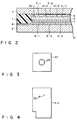
- liquid crystal display 21 is mounted on XY table 20.
- This liquid crystal display has a construction such as that shown in Fig. 2.
- liquid crystal display 21 comprises spacer 1 serving as a support member.
- Translucent glass substrates 2 and 3 are arranged in such a manner as to face each other.
- Common electrode 4 is located between glass substrates 2 and 3, with its one end clamped between spacer 1 and glass substrate 2.
- a plurality of pixel electrodes 5-1, 5-2 ... are arranged on glass substrate 3 such that they face common electrode 4.
- a plurality of color filters 6-1, 6-2 ..., each having one of the three fundamental colors, are arranged between common electrode 4 and glass substrate 2 such that they correspond in location to pixel electrodes 5-1, 5-2..., respectively.
- Located between common electrode 4 and pixels 5-1, 5-2 ... are orientation films 7 and 8 spaced from each other by a predetermined distance.
- Liquid crystal 9 is sealed between orientation films 7 and 8.
- Thin film transistors 10-1, 10-2 ... are attached on glass substrate 3.
- Liquid crystal 9 is supported by use of resin containing fine glass particles, and has a thickness of 5 to 6 ⁇ m.
- XY table 20 has hole 22 formed in the center thereof, and transmitted-illumination unit 23 is located under XY table 20.
- White light P1 emitted from back-light illumination unit 23 is directed to liquid crystal display 21 via hole 22.
- Liquid crystal display 21 is driven, with thin film transistors 10-1, 10-2 ... selectively turned on or off by liquid crystal display-driving unit 24.
- Laser oscillator 30 is a YAG laser oscillator which emits laser beam R used for working materials. This laser oscillator is supplied with power by laser power source 31.
- Optical lens system 32 is arranged in the optical path of laser beam R emitted from laser oscillator 30. This optical lens system serves to convert laser beam R into collimated laser beam Ra, which has a diameter larger than that of laser beam R.
- Mirror 33 is arranged in the optical path located at the output end of optical lens system 32. Laser beam Ra output from optical lens system 32 is reflected by mirror 33 and is therefore directed to beam splitter 34.
- Light source 35 is an alignment beam source which emits white light H serving as an alignment beam.
- White light H emitted from light source 35 is converted by optical lens 36 into a collimated white light beam having an increased diameter, and is then guided to beam splitter 34.
- laser beam Ra and white light beam H travel in the same optical path.
- Slit plate 37 is arranged in the optical path to which laser beam Ra and white light beam H output from beam splitter 34 are directed. As is shown in Fig. 3, slit plate 37 has ring slit 38 formed therein.
- slit plate 37 is made up of glass substrate 39, and metal 40 which is coated on substrate 39 in such a manner as to form ring slit 38. Normally, a plurality of slit plates respectively having ring slits of different diameters are prepared.
- beam-focusing optical system 41 is constituted by a microscope, which includes dichroic mirror 42 and converging lens 43 located in the optical path of the light reflected by dichroic mirror 42.
- Laser beam Ra and white light beam H are first reflected by dichroic mirror 42 and are then converged by converging lens 43.
- beam splitter 44 and focusing lens 45 are arranged in series.
- Illuminator 46 is arranged at a location branching from beam splitter 44. Therefore, light P2 emitted from illuminator 46 is first reflected by beam splitter 44, and is then directed to liquid crystal display 21 through dichroic mirror 42 and converging lens 43. The light reflected by liquid crystal display 21 passes through converging lens 43, dichroic mirror 42, and beam splitter 44, and is guided to focusing lens 45.
- An image sensor, for example, CCD (charge-coupled device) camera 47 is located at the focal position of focusing lens 45, to pick up the image of light crystal display 21 through optical system 41. Image signals output from CCD camera 47 are supplied to monitor television set 48.
- CCD charge-coupled device
- Driving unit 49 used for positioning of beams, causes relative movement between XY table 20 and beam-focusing optical system 41. By utilization of this relative movement, laser beam Ra and white light beam H output from beam-focusing optical system 41 are positioned on a defective portion of liquid crystal display 21 such that their beam rings surrounds the defective portion. The operator performs this operation while observing the beam rings through monitor television set 48.
- liquid crystal display 21 is inspected. If a defect caused by inclusion of foreign matter to liquid crystal display 21 is found in this inspection, liquid crystal display 21 is mounted on XY table 20 such that it is located under beam-focusing optical system 41. In this condition, illuminator 46 emits light beam P2 to beam splitter 44. This light beam is reflected by beam splitter 44, passes through both dichroic mirror 42 and converging lens 43, and then falls on liquid crystal display 21. At the time, CCD camera 47 image-picks up liquid crystal display 21 through dichroic mirror 42, beam splitter 44 and beamfocusing lens 45. The image signals output from CCD camera 47 are supplied to monitor television set 48, which displays an image corresponding to the image signals.
- liquid crystal display 21 is irradiated with white light beam P1 emitted from back-light illumination unit 23 and is driven by liquid crystal display-driving unit 24.
- liquid crystal display 21 different portions are sequentially shown on monitor television set 48 in accordance with the movement of XY table 20. While observing liquid crystal display 21 shown on monitor television set 48, the operator searches the defective portion of liquid crystal display 21. When the location of the defective portion is detected, light source 35 is turned on, to thereby emit white light beam H used for alignment. White light beam H is converted into a collimated beam having a larger diameter, and is guided to slit plate 37 through beam splitter 34. When white light beam H passes through ring slit 38, it is defined as a ring-like white light beam. The ring-like white light beam is guided to beam-focusing optical system 41.
- ring-like white light beam H is reflected by dichroic mirror 42, is converged by converging lens 43, and is made to fall on liquid crystal display 21.
- Liquid crystal display 21 mounted on XY table 20 is moved in the XY plane, with ring-like white light beam H falling thereon, until ring-like white light beam H surrounds foreign matter 50, as is shown in Fig. 4. It should be noted that the diameter of the ring-like white light beam falling on liquid crystal display 21 is determined by slit plate 37 to be employed.
- laser beam R is output by laser oscillator 30.
- optical lens system 32 laser beam R is converted into collimated laser beam Ra whose diameter is larger than that of laser beam R.
- Laser beam Ra is reflected by both mirror 33 and beam splitter 34, and is then guided to slit plate 37.
- laser beam Ra passes through ring slit 38 of slit plate 37, it is defined as a ring-like laser beam.
- Ring-like laser beam thus obtained, is guided to beam-focusing optical system 41.
- ring-like laser beam is reflected by dichroic mirror 42, is converged by converging lens 43, and is made to fall on liquid crystal display 21.
- the location on which ring-like laser beam falls is the same as that on which white light beam H falls.
- ring-like laser beam falls on liquid crystal display 21 in an enlarged scale.
- ring-like laser beam is focused on pixel electrode 5-2 of liquid crystal display 21.
- annular region 51 which is irradiated with ring-like laser beam is burnt away, in other words, removed from pixel electrode 5-2.
- Small region 52 located inside of annular region 51 is electrically insulated from the region located outside of annular region 52. Even when liquid crystal display-driving unit 24 does not apply any voltage between common electrode 4 and pixel electrode 5-2, a voltage is applied between small region 52 of pixel electrode 5-2 and common electrode 4.
- white light P2 emitted from back-light illumination unit 23 toward liquid crystal display 21 passes through small region 52 and its corresponding region of color filter 6-2, this does not causes any problem in practice, since the area of region 52 is very small; it is less than one tenth of the area of one pixel.
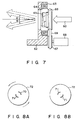
- the present invention is not limited to the embodiment mentioned above. It can be modified in various manners without departing from the spirit and scope of the invention. For instance, an annular region located around foreign matter can be removed by scanning it with laser beam spot 60 in the direction indicated in Fig. 6. In this fashion as well, a portion which is short-circuited due to inclusion of foreign matter can be electrically insulated from the other portions.
- the scanning apparatus shown in Fig. 7 can be employed. As is shown in Fig. 7, the scanning apparatus comprises housing 64 rotatably attached to base 62 by bearings 63. Prism 65 is held by housing 64. Pulley 66 is fixed to housing 64, and motor 68 is provided in the vicinity of pulley 66. Pulley 67 is attached to the rotatable shaft of motor 68. Belt 69 is wound around pulleys 66 and 67.
- laser beam 60 can describe the track shown in Fig. 6.
- slit plate 72 shown in Fig. 8 may be employed as a means for producing a ring-like beam.
- slit plate 72 has a pair of arcuate slits, each of which is about one fourth of a complete circle.
- slit plate 72 is rotated 90° from the state shown in Fig. 8A to the state shown in Fig. 8B, to thereby produce a ring-like beam.
- white light beam H used as an alignment beam travels through the same optical path as that of the laser beam deflected by beam splitter 34.
- white light beam H can be directed to liquid crystal display 21 through a different optical path to that of the laser beam.
Landscapes
- Physics & Mathematics (AREA)
- Nonlinear Science (AREA)
- Chemical & Material Sciences (AREA)
- Crystallography & Structural Chemistry (AREA)
- General Physics & Mathematics (AREA)
- Optics & Photonics (AREA)
- Mathematical Physics (AREA)
- Liquid Crystal (AREA)
- Laser Beam Processing (AREA)
Claims (10)
- Verfahren zum Instandsetzen einer defekten Flüssigkristallanzeige der Art mit einer gemeinsamen bzw. Sammelelektrode, der Sammelelektrode zugewandten Pixelelektroden und einem zwischen Sammel- und Pixelelektroden eingesiegelten Flüssigkristall, wobei der Defekt in einem leitfähigen Fremdkörper besteht, welcher die Sammelelektrode und die Pixelelektrode gegeneinander kurzschließt, gekennzeichnet durch folgende Schritte:
Bestrahlen der zur Sammelelektrode kurzgeschlossenen Pixelelektrode mit einem Laserstrahl in der Weise, daß mindestens ein ringartiger Bereich der Pixelelektrode, der einer Ringlinie entspricht, die den den Fremdkörper berührenden Abschnitt der Pixelelektrode vollständig umschließt, mittels des Laserstrahls entfernt wird, so daß der innerhalb des Ringlinienbereichs liegende Bereich der Pixelelektrode von dem außerhalb des Ringlinienbereichs liegenden Bereich der Pixelelektrode elektrisch getrennt oder isoliert wird. - Vorrichtung zum Instandsetzen einer Flüssigkristallanzeige mit einer gemeinsamen oder Sammelelektrode, mehreren der Sammelelektrode zugewandten Pixelelektroden und einem zwischen Sammel- und Pixelelektroden eingesiegelten Flüssigkristall, wobei die Anzeige einen Defekt in Form eines leitfähigen Fremdkörpers aufweist, welcher die Sammelelektrode und die Pixelelektrode gegeneinander kurzschließt, gekennzeichnet durch
eine Laseroszillatoreinheit (30) zum Erzeugen eines Laserstrahls,
eine Ausrichtstrahlquelleneinheit (35) zum Abgeben eines Ausrichtstrahls, der für Ausrichtung des von der Laseroszillatoreinheit erzeugten Laserstrahls benutzt wird,
eine erste optische Einheit (37) zum Formell des Laserstrahls und des Ausrichtstrahls in der Weise, daß der Laserstrahl und der Ausrichtstrahl einen ringförmigen Querschnitt aufweisen,
eine XY-Trägereinheit (20), auf welcher die Flüssigkristallanzeige montiert und welche in, einer XY-Ebene verschiebbar ist,
eine Ansteuereinheit (24) zum Ansteuern der Flüssigkristallanzeige,
eine zweite optische Einheit (41) zum Fokussieren des Laserstrahls und des Ausrichtstrahls mit ringförmigen Querschnitten auf einen vorbestimmten Abschnitt der Flüssigkristallanzeige,
eine Beleuchtungseinheit (46) zum Beleuchten der Flüssigkristallanzeige durch Richten von Licht auf diese über die zweite optische Einheit,
eine Bildsensoreinheit (47) zum Aufnehmen eines Bilds der Flüssigkristallanzeige über die zweite optische Einheit zwecks Erzeugung eines Bildsignals, (und)
eine Monitoreinheit (48) zum Sichtbarmachen des von der Bildsensoreinheit gelieferten Bildsignals zwecks Ermöglichung einer Detektion der mit dem Fremdkörper in Berührung stehenden Pixelelektrode,
wobei ein ringartiger Bereich der Pixelelektrode, welcher den den Fremdkörper berührenden Elektrodenabschnitt umschließt, mittels des Laserstrahls entfernt werden kann, um den den Fremdkörper berührenden Pixelelektrodenabschnitt von dem außerhalb des ringartigen Bereichs liegenden Pixelelektrodenabschnitt elektrisch zu trennen bzw. zu isolieren. - Vorrichtung nach Anspruch 2, dadurch gekennzeichnet, daß der von der Ausrichtstrahlquelleneinheit (35) abgegebene Ausrichtstrahl ein weißer Lichtstrahl ist.
- Vorrichtung nach Anspruch 2, dadurch gekennzeichnet, daß die erste optische Einheit (37) eine Schlitzscheibe umfaßt, die eine Glasscheibe (39) und eine auf die Glasscheibe aufgetragene Metallschicht (40) mit einem dem ringförmigen Querschnitt entsprechenden Ringschlitz aufweist.
- Vorrichtung nach Anspruch 2, dadurch gekennzeichnet, daß die erste optische Einheit eine Anzahl von Schlitzscheiben umfaßt, welche Ringschlitze unterschiedlicher Durchmesser aufweisen und welche selektiv verwendet werden.
- Vorrichtung nach Anspruch 2, dadurch gekennzeichnet, daß die erste optische Einheit ein Prisma (65) zum Brechen des Laserstrahls unter einem vorbestimmten Winkel, ein drehbares Gehäuse (62) zum Halten des Prismas, einen Motor (68) und einen Riemen (69) zum Übertragen des Drehmoments des Motors zum Gehäuse umfaßt.
- Vorrichtung nach Anspruch 2, dadurch gekennzeichnet, daß die erste optische Einheit eine Schlitzscheibe (72) mit einem bogenförmigen Schlitz und eine Einheit zum Drehen der Schlitzscheibe über einen vorbestimmten Winkel umfaßt.
- Vorrichtung nach Anspruch 2, dadurch gekennzeichnet, daß die XY-Trägereinheit ein XY-Tisch (20) ist.
- Vorrichtung nach Anspruch 2, dadurch gekennzeichnet, daß die erste optische Einheit einen dichroitischen Spiegel (42) zum Reflektieren des Laserstrahls und des Ausrichtstrahls, die von einer Schlitzscheibe (zu)geleitet werden, und eine Sammellinse (43) zum Konvergieren des Laserstrahls und des Ausrichtstrahls, die vom dichroitischen Spiegel reflektiert werden, umfaßt.
- Vorrichtung nach Anspruch 2, dadurch gekennzeichnet, daß die Bildsensoreinheit eilt Festkörper-Ladungsverschiebeelement (47) aufweist.
Applications Claiming Priority (4)
| Application Number | Priority Date | Filing Date | Title |
|---|---|---|---|
| JP270203/88 | 1988-10-26 | ||
| JP27020388A JPH073625B2 (ja) | 1988-10-26 | 1988-10-26 | 液晶ディスプレイの修正方法 |
| JP20475789A JPH0369914A (ja) | 1989-08-09 | 1989-08-09 | 液晶ディスプレイの修正装置 |
| JP204757/89 | 1989-08-09 |
Publications (3)
| Publication Number | Publication Date |
|---|---|
| EP0366459A2 EP0366459A2 (de) | 1990-05-02 |
| EP0366459A3 EP0366459A3 (de) | 1991-07-31 |
| EP0366459B1 true EP0366459B1 (de) | 1994-05-04 |
Family
ID=26514628
Family Applications (1)
| Application Number | Title | Priority Date | Filing Date |
|---|---|---|---|
| EP89311040A Expired - Lifetime EP0366459B1 (de) | 1988-10-26 | 1989-10-26 | Verfahren zur Reparatur einer Flüssigkristallanzeige und Gerät für die Verwendung dieses Verfahrens |
Country Status (3)
| Country | Link |
|---|---|
| US (1) | US5017755A (de) |
| EP (1) | EP0366459B1 (de) |
| DE (1) | DE68915115T2 (de) |
Families Citing this family (54)
| Publication number | Priority date | Publication date | Assignee | Title |
|---|---|---|---|---|
| DE4013195A1 (de) * | 1990-04-25 | 1991-10-31 | Lambda Physik Forschung | Vorrichtung und verfahren zum ueberwachen der bearbeitung eines werkstueckes mit gepulster laserstrahlung |
| JP3150322B2 (ja) * | 1990-05-18 | 2001-03-26 | 株式会社日立製作所 | レーザによる配線切断加工方法及びレーザ加工装置 |
| US5171963A (en) * | 1990-05-21 | 1992-12-15 | Ntn Corporation | Laser processing device and laser processing method |
| US5285150A (en) * | 1990-11-26 | 1994-02-08 | Photon Dynamics, Inc. | Method and apparatus for testing LCD panel array |
| US5081687A (en) | 1990-11-30 | 1992-01-14 | Photon Dynamics, Inc. | Method and apparatus for testing LCD panel array prior to shorting bar removal |
| JPH04208834A (ja) * | 1990-12-04 | 1992-07-30 | Ezel Inc | 液晶パネルの検査方法 |
| JP2766563B2 (ja) * | 1991-03-27 | 1998-06-18 | シャープ株式会社 | 液晶表示装置 |
| US5164565A (en) * | 1991-04-18 | 1992-11-17 | Photon Dynamics, Inc. | Laser-based system for material deposition and removal |
| US5168141A (en) * | 1991-06-14 | 1992-12-01 | General Electric Company | Vision guided laser welding |
| US5175504A (en) * | 1991-06-17 | 1992-12-29 | Photon Dynamics, Inc. | Method and apparatus for automatically inspecting and repairing a simple matrix circuit panel |
| US5235272A (en) * | 1991-06-17 | 1993-08-10 | Photon Dynamics, Inc. | Method and apparatus for automatically inspecting and repairing an active matrix LCD panel |
| US5432461A (en) * | 1991-06-28 | 1995-07-11 | Photon Dynamics, Inc. | Method of testing active matrix liquid crystal display substrates |
| US5465052A (en) * | 1991-09-10 | 1995-11-07 | Photon Dynamics, Inc. | Method of testing liquid crystal display substrates |
| US5459409A (en) * | 1991-09-10 | 1995-10-17 | Photon Dynamics, Inc. | Testing device for liquid crystal display base plate |
| US5444385A (en) * | 1991-09-10 | 1995-08-22 | Photon Dynamics, Inc. | Testing apparatus for liquid crystal display substrates |
| US5504438A (en) * | 1991-09-10 | 1996-04-02 | Photon Dynamics, Inc. | Testing method for imaging defects in a liquid crystal display substrate |
| US5543729A (en) * | 1991-09-10 | 1996-08-06 | Photon Dynamics, Inc. | Testing apparatus and connector for liquid crystal display substrates |
| US5241419A (en) * | 1992-01-27 | 1993-08-31 | General Electric Company | Co-axial viewing device for lasers |
| US5514850A (en) * | 1992-06-30 | 1996-05-07 | Sharp Kabushiki Kaisha | Defect compensation method for smoothing a surface of a transparent plate with an ArF excimer laser beam |
| JP3293136B2 (ja) * | 1993-06-04 | 2002-06-17 | セイコーエプソン株式会社 | レーザ加工装置及びレーザ加工方法 |
| US5518956A (en) * | 1993-09-02 | 1996-05-21 | General Electric Company | Method of isolating vertical shorts in an electronic array using laser ablation |
| JP3179963B2 (ja) * | 1994-04-26 | 2001-06-25 | 松下電器産業株式会社 | レーザ加工装置とレーザ加工方法 |
| US5932119A (en) * | 1996-01-05 | 1999-08-03 | Lazare Kaplan International, Inc. | Laser marking system |
| JP3292058B2 (ja) * | 1996-10-01 | 2002-06-17 | 三菱電機株式会社 | レーザ光による配線基板の加工方法及びその装置 |
| JP3063688B2 (ja) * | 1997-07-30 | 2000-07-12 | 日本電気株式会社 | レーザ加工装置及びその制御方法並びにその制御プログラムを記録した記録媒体 |
| JP4659300B2 (ja) * | 2000-09-13 | 2011-03-30 | 浜松ホトニクス株式会社 | レーザ加工方法及び半導体チップの製造方法 |
| US6465767B2 (en) * | 2000-12-27 | 2002-10-15 | General Electric Company | Photomultiplier tube reprocessing |
| CN100355031C (zh) | 2002-03-12 | 2007-12-12 | 浜松光子学株式会社 | 基板的分割方法 |
| JP2005032576A (ja) * | 2003-07-04 | 2005-02-03 | Fuji Electric Holdings Co Ltd | 多色有機発光表示素子の修復方法および修復装置 |
| JP2005276600A (ja) * | 2004-03-24 | 2005-10-06 | Hitachi Ltd | 有機エレクトロルミネセンス表示装置の製造方法 |
| JP4688525B2 (ja) * | 2004-09-27 | 2011-05-25 | 株式会社 日立ディスプレイズ | パターン修正装置および表示装置の製造方法 |
| US7317325B2 (en) * | 2004-12-09 | 2008-01-08 | Applied Materials, Inc. | Line short localization in LCD pixel arrays |
| CN100353222C (zh) * | 2005-02-21 | 2007-12-05 | 广辉电子股份有限公司 | 液晶显示器面板的制造方法 |
| GB0625001D0 (en) * | 2006-12-14 | 2007-01-24 | Plastic Logic Ltd | Short isolation |
| ATE477876T1 (de) * | 2008-05-02 | 2010-09-15 | Leister Process Tech | Verfahren und laservorrichtung zum bearbeiten und/oder verbinden von werkstücken mittels laserstrahlung mit leistungswirk- und pilotlaser und mindestens einem diffraktiven optischen element |
| US10303035B2 (en) | 2009-12-22 | 2019-05-28 | View, Inc. | Self-contained EC IGU |
| US8164818B2 (en) | 2010-11-08 | 2012-04-24 | Soladigm, Inc. | Electrochromic window fabrication methods |
| US10180606B2 (en) | 2010-12-08 | 2019-01-15 | View, Inc. | Connectors for smart windows |
| US8643933B2 (en) | 2011-12-14 | 2014-02-04 | View, Inc. | Connectors for smart windows |
| US10175549B2 (en) | 2011-03-16 | 2019-01-08 | View, Inc. | Connectors for smart windows |
| US9454055B2 (en) | 2011-03-16 | 2016-09-27 | View, Inc. | Multipurpose controller for multistate windows |
| US9885934B2 (en) * | 2011-09-14 | 2018-02-06 | View, Inc. | Portable defect mitigators for electrochromic windows |
| EP2756289B1 (de) | 2011-09-14 | 2023-03-29 | View, Inc. | Tragbarer fehlerreduzierer für elektrochrome fenster |
| US11719039B2 (en) | 2011-12-14 | 2023-08-08 | View, Inc. | Connectors for smart windows |
| WO2013138535A1 (en) | 2012-03-13 | 2013-09-19 | View, Inc. | Pinhole mitigation for optical devices |
| US9341912B2 (en) | 2012-03-13 | 2016-05-17 | View, Inc. | Multi-zone EC windows |
| CN107552950B (zh) | 2012-05-18 | 2021-01-01 | 唯景公司 | 限制光学装置中的缺陷 |
| US11255120B2 (en) | 2012-05-25 | 2022-02-22 | View, Inc. | Tester and electrical connectors for insulated glass units |
| US10288971B2 (en) | 2012-08-23 | 2019-05-14 | View, Inc. | Photonic-powered EC devices |
| US9304090B2 (en) * | 2013-03-11 | 2016-04-05 | Electro Scientific Industries, Inc. | Systems and methods for providing polarization compensated multi-spectral laser repair of liquid crystal display panels |
| US9405254B2 (en) * | 2013-11-26 | 2016-08-02 | Xerox Corporation | Device for uniform light intensity generation |
| DE102014108259A1 (de) * | 2014-06-12 | 2015-12-17 | Scanlab Ag | Vorrichtung zur Lasermaterialbearbeitung |
| US11320713B2 (en) | 2017-02-16 | 2022-05-03 | View, Inc. | Solar power dynamic glass for heating and cooling buildings |
| CN112540471B (zh) * | 2020-12-04 | 2021-11-23 | Tcl华星光电技术有限公司 | 显示面板、点灯测试方法、点灯测试装置 |
Family Cites Families (6)
| Publication number | Priority date | Publication date | Assignee | Title |
|---|---|---|---|---|
| US3947093A (en) * | 1973-06-28 | 1976-03-30 | Canon Kabushiki Kaisha | Optical device for producing a minute light beam |
| US3972599A (en) * | 1974-09-16 | 1976-08-03 | Caterpillar Tractor Co. | Method and apparatus for focussing laser beams |
| US4190759A (en) * | 1975-08-27 | 1980-02-26 | Hitachi, Ltd. | Processing of photomask |
| JPS5641088A (en) * | 1979-09-12 | 1981-04-17 | Hitachi Ltd | Monitoring device for laser light axis |
| JPH0774866B2 (ja) * | 1982-10-06 | 1995-08-09 | セイコー電子工業株式会社 | 液晶表示器の製造方法 |
| JP2698357B2 (ja) * | 1987-08-17 | 1998-01-19 | キヤノン株式会社 | 電極間の短絡部分離法及び液晶パネルの製造法 |
-
1989
- 1989-10-20 US US07/424,695 patent/US5017755A/en not_active Expired - Fee Related
- 1989-10-26 EP EP89311040A patent/EP0366459B1/de not_active Expired - Lifetime
- 1989-10-26 DE DE68915115T patent/DE68915115T2/de not_active Expired - Fee Related
Also Published As
| Publication number | Publication date |
|---|---|
| DE68915115D1 (de) | 1994-06-09 |
| EP0366459A2 (de) | 1990-05-02 |
| DE68915115T2 (de) | 1994-10-13 |
| US5017755A (en) | 1991-05-21 |
| EP0366459A3 (de) | 1991-07-31 |
Similar Documents
| Publication | Publication Date | Title |
|---|---|---|
| EP0366459B1 (de) | Verfahren zur Reparatur einer Flüssigkristallanzeige und Gerät für die Verwendung dieses Verfahrens | |
| US6639201B2 (en) | Spot grid array imaging system | |
| JP4337999B2 (ja) | 焦点位置制御機構及び方法、並びに、半導体ウェハの検査装置及び方法 | |
| JP3199481B2 (ja) | 液晶ディスプレイ基板の検査装置 | |
| KR20070085258A (ko) | 다이렉트 이미지 기술을 사용하는 평판 매체의 광학적 검사 | |
| CN114074217B (zh) | 激光加工装置 | |
| EP1393115B1 (de) | Systeme und verfahren zum scannen einer probe mit einem lichtstrahl | |
| US4448527A (en) | Method and apparatus for detecting surface defects in mechanical workpieces | |
| JP2016024195A (ja) | テレセントリック明視野および環状暗視野のシームレス融合型照明 | |
| KR930001517B1 (ko) | 레이저로 금속도체를 접합 가공하는 방법 및 그 장치 | |
| GB2095398A (en) | Detecting surface defects in workpieces | |
| JPH05256793A (ja) | 液晶ディスプレイ基板の検査装置 | |
| JPH0369914A (ja) | 液晶ディスプレイの修正装置 | |
| JPH09210660A (ja) | 撮像式検査装置 | |
| KR20230004260A (ko) | 레이저 가공 장치 및 레이저 가공 방법 | |
| US20130208270A1 (en) | Defect inspecting apparatus and defect inspecting method | |
| JP2001264266A (ja) | 基板検査装置 | |
| EP0526734A2 (de) | Kontaktloser Fühler und ihn verwendende Untersuchungsvorrichtung für Anordnungen mit aktiver Matrix | |
| JPH06331945A (ja) | 薄型表示機器の検査装置及び欠陥修正装置 | |
| JPH05288640A (ja) | カラーフィルターの検査方法 | |
| JPH08304298A (ja) | 赤外検査装置 | |
| JPH04239149A (ja) | 結晶劈開面検査用顕微鏡システム | |
| KR910006368B1 (ko) | 반도체장치의 검사방법 및 그 검사장치 | |
| JP3776628B2 (ja) | 画像処理装置を用いる検査方法 | |
| KR0183700B1 (ko) | 음극선관의 패널 검사장치 |
Legal Events
| Date | Code | Title | Description |
|---|---|---|---|
| PUAI | Public reference made under article 153(3) epc to a published international application that has entered the european phase |
Free format text: ORIGINAL CODE: 0009012 |
|
| 17P | Request for examination filed |
Effective date: 19891116 |
|
| AK | Designated contracting states |
Kind code of ref document: A2 Designated state(s): DE FR NL |
|
| PUAL | Search report despatched |
Free format text: ORIGINAL CODE: 0009013 |
|
| AK | Designated contracting states |
Kind code of ref document: A3 Designated state(s): DE FR NL |
|
| 17Q | First examination report despatched |
Effective date: 19930308 |
|
| GRAA | (expected) grant |
Free format text: ORIGINAL CODE: 0009210 |
|
| AK | Designated contracting states |
Kind code of ref document: B1 Designated state(s): DE FR NL |
|
| REF | Corresponds to: |
Ref document number: 68915115 Country of ref document: DE Date of ref document: 19940609 |
|
| ET | Fr: translation filed | ||
| PLBE | No opposition filed within time limit |
Free format text: ORIGINAL CODE: 0009261 |
|
| STAA | Information on the status of an ep patent application or granted ep patent |
Free format text: STATUS: NO OPPOSITION FILED WITHIN TIME LIMIT |
|
| 26N | No opposition filed | ||
| PGFP | Annual fee paid to national office [announced via postgrant information from national office to epo] |
Ref country code: FR Payment date: 19961009 Year of fee payment: 8 |
|
| PGFP | Annual fee paid to national office [announced via postgrant information from national office to epo] |
Ref country code: DE Payment date: 19961104 Year of fee payment: 8 |
|
| PG25 | Lapsed in a contracting state [announced via postgrant information from national office to epo] |
Ref country code: FR Free format text: THE PATENT HAS BEEN ANNULLED BY A DECISION OF A NATIONAL AUTHORITY Effective date: 19971031 |
|
| PG25 | Lapsed in a contracting state [announced via postgrant information from national office to epo] |
Ref country code: DE Free format text: LAPSE BECAUSE OF NON-PAYMENT OF DUE FEES Effective date: 19980701 |
|
| REG | Reference to a national code |
Ref country code: FR Ref legal event code: ST |
|
| PGFP | Annual fee paid to national office [announced via postgrant information from national office to epo] |
Ref country code: NL Payment date: 19981028 Year of fee payment: 10 |
|
| PG25 | Lapsed in a contracting state [announced via postgrant information from national office to epo] |
Ref country code: NL Free format text: LAPSE BECAUSE OF NON-PAYMENT OF DUE FEES Effective date: 20000501 |
|
| NLV4 | Nl: lapsed or anulled due to non-payment of the annual fee |
Effective date: 20000501 |