EP0362050A2 - Carte à mémoire - Google Patents
Carte à mémoire Download PDFInfo
- Publication number
- EP0362050A2 EP0362050A2 EP89402634A EP89402634A EP0362050A2 EP 0362050 A2 EP0362050 A2 EP 0362050A2 EP 89402634 A EP89402634 A EP 89402634A EP 89402634 A EP89402634 A EP 89402634A EP 0362050 A2 EP0362050 A2 EP 0362050A2
- Authority
- EP
- European Patent Office
- Prior art keywords
- memory
- card
- bits
- memory card
- write
- Prior art date
- Legal status (The legal status is an assumption and is not a legal conclusion. Google has not performed a legal analysis and makes no representation as to the accuracy of the status listed.)
- Granted
Links
Images


Classifications
-
- G—PHYSICS
- G06—COMPUTING; CALCULATING OR COUNTING
- G06K—GRAPHICAL DATA READING; PRESENTATION OF DATA; RECORD CARRIERS; HANDLING RECORD CARRIERS
- G06K19/00—Record carriers for use with machines and with at least a part designed to carry digital markings
- G06K19/06—Record carriers for use with machines and with at least a part designed to carry digital markings characterised by the kind of the digital marking, e.g. shape, nature, code
- G06K19/067—Record carriers with conductive marks, printed circuits or semiconductor circuit elements, e.g. credit or identity cards also with resonating or responding marks without active components
- G06K19/07—Record carriers with conductive marks, printed circuits or semiconductor circuit elements, e.g. credit or identity cards also with resonating or responding marks without active components with integrated circuit chips
-
- G—PHYSICS
- G06—COMPUTING; CALCULATING OR COUNTING
- G06K—GRAPHICAL DATA READING; PRESENTATION OF DATA; RECORD CARRIERS; HANDLING RECORD CARRIERS
- G06K7/00—Methods or arrangements for sensing record carriers, e.g. for reading patterns
- G06K7/0008—General problems related to the reading of electronic memory record carriers, independent of its reading method, e.g. power transfer
Definitions
- the present invention generally relates to memory cards, and more particularly to a memory card which has a memory function and has a shape of a credit card, for example.
- a memory card which has no central processing unit (CPU) but has a built-in memory such as a random access memory (RAM) and a read only memory (ROM).
- the memory card uses a data bus having a bit width of eight bits or sixteen bits, and there are proposals to use a data bus having a bit width which is a multiple of eight such as thirty-two bits and sixty-four bits.
- a card write/read apparatus When such a memory card is loaded into a card write and/or read apparatus (hereinafter simply referred to as a card write/read apparatus), it is possible to write an arbitrary information to the memory card and/or read a prestored information from the memory card.
- FIG.1 shows an example of a conventional memory card.
- the memory card comprises an input buffer 100, a memory 101, an input/output buffer 102, and terminals 103 through 107.
- An address signal ADR is applied to the terminal 103
- a write enable signal WE is applied to the terminal 104
- a chip select signal CS is applied to the terminal 105
- an output enable signal OE is applied to the terminal 106.
- a write datum which is to be written into the memory 101 and a read datum which is read out from the memory 101 are input and output via the data input/output terminal 107.
- the input of the write datum is controlled by the input/output buffer 102 in response to the write enable signal WE.
- the output of the read datum is controlled by the input/output buffer 102 in response to the output enable signal OE.
- the bit width of the data input/output terminal 107 determines the card write/read apparatus to which the memory card may be loaded.
- a memory card which has a data bus with a bit width of eight bits is used exclusively on a card write/read apparatus having a data bus with a bit width of eight bits.
- a memory card which has a data bus with a bit width of sixteen bits is used exclusively on a card write/read apparatus having a data bus with a bit width of sixteen bits.
- the bit width of the data bus of the card write/read apparatus conventionally determines the memory cards which may be used thereon.
- a memory card which has a data bus with a bit width different from that of the card write/read apparatus cannot be used on this card write/read apparatus.
- FIG.2 shows another example of the conventional memory card.
- the memory card shown in FIG.2 has a data bus with a bit width of sixteen bits.
- the memory card comprises two 256 k x 8 bit RAMs 101 L and 101 H , a terminal 105 L for receiving a chip select signal CS0 which selects a lower byte (that is, the RAM 101 L ), and a terminal 105 H for receiving a chip select signal CS1 which selects an upper byte (that is, the RAM 101 H ).
- Table 1 shows an operation mode of the memory card determined by the chip select signals CS0 and CS1, where "H” denotes a high logic level and "L” denotes a low logic level.
- Table 1 CS1 CS0 Operation Mode H H Non-Select H L Lower Byte Select L H Upper Byte Select L L Word Access
- Another and more specific object of the present invention is to provide a memory card for use on a card write and/or read apparatus which has a data bus with an arbitrary bit width and writes and/or reads a datum to and/or from the memory card, comprising data input/output terminal means, memory means having a data bus with a bit width of at least n bits for coupling to the data bus of the card write and/or read apparatus via the data input/output terminal means, address input terminal means for receiving an address signal, first input terminal means for receiving a first chip select signal which selects a first byte, second input terminal means for receiving a second chip select signal which selects a second byte, and decoder means for determining a bit width of the data bus of the memory means to be used for data communication between the card write and/or read apparatus to one of n bits and n/N bits based on the first and second chip select signals and one or a plurality of arbitrary bits of the address signal by supplying control signals to the memory means, where n, N and
- the memory card of the present invention it is possible to use the memory card on card write and/or read apparatus having data buses with different bit widths. In addition, it is possible to extend the functions of the card write and/or read apparatus without the need to modify the design of the card write and/or read apparatus.
- a memory card comprises a memory means 1 which has a data bus with a bit width of at least n bits, an address input terminal 2 for receiving an address signal ADR, an n-bit data output terminal 5 for outputting a read datum which is read out from the memory means 1, a first input terminal 7 for receiving a first chip select signal CS0 which selects a first byte, a second input terminal 8 for receiving a second chip select signal CSN which selects a second byte, and a decoder circuit 9.
- the decoder circuit 9 generates control signals CE0 and CEN based on the first and second chip select signals CS0 and CSN which are received via the first and second input terminals 7 and 8 and a predetermined bit of the address signal ADR.
- the control signals CS0 and CSN control the bit width of the memory means 1 to n bits or n/N bits depending on a bit width of a data bus of a card write/read apparatus on which the memory card is to be used, where n, N and n/N are positive integers. Therefore, this memory card can be used on a card write/read apparatus which has a data bus with a bit width of n bits and a card write/read apparatus which has a data bus with a bit width of n/N bits.
- the memory card according to the present invention can be used on a card write/read apparatus which has a data bus with a bit width of eight bits and a card write/read apparatus which has a data bus with a bit width of sixteen bits.
- a memory card shown in FIG.4 generally comprises an input buffer 11, 256 k x 8 bit RAMs 12 and 13, an input/output buffer 14, a decoder circuit 15, and terminals 16 through 21.
- Bits A0 through A18 of the address signal ADR are applied to the terminal 16, and the bit A0 is supplied to the decoder circuit 15 while the remaining bits A1 through A18 are supplied to the input buffer 11.
- a write enable signal WE is applied to the terminal 17 and is supplied to each of the input buffer 11, the RAMs 12 and 13 and the input/output buffer 14.
- An output enable signal OE is applied to the terminal 18 and is supplied to the input/output buffer 14.
- a chip select signal CS1 which selects the upper byte (that is, the RAM 12) is applied to the terminal 19 and is supplied to the decoder circuit 15.
- a chip select signal CS0 which selects the lower byte (that is, the RAM 13) is applied to the terminal 20 and is supplied to the decoder circuit 15.
- the decoder circuit 15 Based on the bit A0 and the chip select signals CS0 and CS1, the decoder circuit 15 generates control signals CE0 and CE1 which are supplied to the respective RAMs 12 and 13.
- the memory bit width is set to sixteen bits regardless of the logic value of the bit A0.
- the memory bit width is set to eight bits. When the memory bit width is set to eight bits, one of the the RAMs 12 and 13 is used depending on the logic value of the bit A0.
- the RAM 12 is selectively used when the bit A0 has a low logic level and the logic values of the chip select signals CS0 and CS1 are mutually different.
- Table 2 shows the relationships of the chip select signals CS0 and CS1, the bit A0 and the control signals CS0 and CS1, where "H” and “L” respectively denote high and low logic levels and "X” denotes a don't care.
- Table 2 CS1 CS0 A0 CE1 CE0 H H X H H H L L H L H L H L H L H L H L L L X L
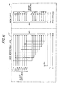
- FIG.5 is a diagram for explaining the use of the first embodiment of the memory card on a card write/read apparatus which has a data bus with a bit width of eight bits.
- the 8-bit data bus of the card write/read apparatus 40 is connected to a terminal 30 as if it were a 16-bit data bus. That is, the apparent bit width of the data bus is sixteen bits.
- the terminal 30 of the card write/read apparatus 40 is connected to the data input/output terminal 21 of the memory card 41.
- terminals 31, 32 and 33 of the card write/read apparatus are respectively connected to the corresponding terminals 19, 160 and 20 of the memory card 41.
- the terminal 31 is connected to a power source voltage Vcc and is thus constantly fixed to the high logic level.
- the bit A0 of the address signal ADR is supplied to the terminal 32, and the chip select signal CS is supplied to the terminal 33.
- the memory card 41 is used on the card write/read apparatus 40 as if it were a memory card having a data bus with a bit width of eight bits. Furthermore, there is no need to provide a decoder circuit or the like within the card write/read apparatus 40, and it is unnecessary to make a design modification of the card write/read apparatus 40 depending on the bit width of the data bus of the memory card.
- the memory card 41 can be used on a card write/read apparatus which has a data bus with a bit width of eight bits and a card write/read apparatus which has a data bus with a bit width of sixteen bits, without making a design modification on the card write/read apparatuses. For this reason, a memory card which has a data bus with a bit width of eight bits can still be used on the card write/read apparatus which has the data bus with the bit width of eight bits, and a memory card which has a data bus with a bit width of sixteen bits can still be used on the card write/read apparatus which has the data bus with the bit width of sixteen bits.
- Table 3 shows the operation mode of the memory card, the state of the data input/output terminal 21 and the state of the power source current which are determined on the signals CS0 and CS1, A0, OE and WE.
- "High Imp” denotes a high impedance state, and the same designations are used as in Table 2.
- Table 3 is divided into part A and part B due to the limited space.
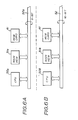
- FIGS.6A and 6B respectively show embodiments of the use of the first embodiment of the memory card.
- FIG.6A shows a case where the memory card 41 is used on a card write/read apparatus which has a CPU 50a, a main memory device 51a and an 8-bit data bus 52a.
- FIG.6B shows a case where the memory card 41 is used on a card write/read apparatus which has a CPU 50b, a main memory device 51b and a 16-bit data bus 52b.
- FIG.8 shows an embodiment of the decoder circuit 15 shown in FIG.4.
- the decoder circuit 15 comprises a NAND circuit 151, OR circuits 152 and 153, and AND circuits 154 and 155 which are connected as shown.
- the control signal CE0 is output from the OR circuit 153
- the control signal CE1 is output from the AND circuit 154.
- FIGS.9(A) through 9(E) show timing charts for explaining the operation of the decoder circuit 15 shown in FIG.8 for different input signals CS0 and CS1 and A0.
- FIGS.9(A) and 9(B) respectively show the chip select signals CS0 and CS1
- FIG.9(C) shows the bit A0 of the address signal ADR.
- FIGS.9(D) and 9(E) respectively show the control signals CE1 and CE0 output from the decoder circuit 15.
- a memory card comprises 8-bit memories M0 through M7, a decoder circuit 61, data input/output terminals 62a and 62b, and terminals 63 through 70.
- An upper byte made up of bits I/O0 through I/O7 of an input/output datum I/O0 through I/O15 is input and output via the data input/output terminal 62a, and a lower byte made up of bits I/O8 through I/O15 of the input/output datum I/O0 through I/O15 is input and output via the data input/output terminal 62b.
- a write enable signal WE is applied to the terminal 63, and an output enable signal OE is applied to the terminal 64.
- Chip select signals CS1 and CS0 are respectively applied to the terminals 65 and 66.
- Out of an address signal ADR made up of bits A0 through A N+3 bits A0, A N+2 and A N+3 are respectively applied to the corresponding terminals 67, 68 and 69, while the remaining bits A1 through A N+1 are applied to the terminal 70.
- no input buffer nor input/output buffer which correspond to those of the first embodiment. However, it is possible to obtain substantially the same effects as those obtainable by the first embodiment.
- the bit width of the data bus is of course not limited to eight bits and sixteen bits.
- the data buses may have bit widths of eight bits, sixteen bits and thirty-two bits.
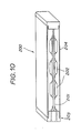
- FIG.10 generally shows an embodiment of an external appearance of the memory card.
- a memory card 200 comprises a printed circuit 201, memory integrated circuits (ICs) 202 connected to the printed circuit 201, an interface connector 203, a cover 204 and the like.
- ICs memory integrated circuits
Landscapes
- Engineering & Computer Science (AREA)
- Physics & Mathematics (AREA)
- General Physics & Mathematics (AREA)
- Theoretical Computer Science (AREA)
- Artificial Intelligence (AREA)
- Computer Vision & Pattern Recognition (AREA)
- Computer Hardware Design (AREA)
- Microelectronics & Electronic Packaging (AREA)
- Bus Control (AREA)
- Memory System (AREA)
- Storage Device Security (AREA)
Applications Claiming Priority (2)
| Application Number | Priority Date | Filing Date | Title |
|---|---|---|---|
| JP63242950A JP2539012B2 (ja) | 1988-09-28 | 1988-09-28 | メモリカ―ド |
| JP242950/88 | 1988-09-28 |
Publications (3)
| Publication Number | Publication Date |
|---|---|
| EP0362050A2 true EP0362050A2 (fr) | 1990-04-04 |
| EP0362050A3 EP0362050A3 (fr) | 1991-04-03 |
| EP0362050B1 EP0362050B1 (fr) | 1994-11-17 |
Family
ID=17096636
Family Applications (1)
| Application Number | Title | Priority Date | Filing Date |
|---|---|---|---|
| EP89402634A Expired - Lifetime EP0362050B1 (fr) | 1988-09-28 | 1989-09-26 | Carte à mémoire |
Country Status (5)
| Country | Link |
|---|---|
| US (1) | US5025415A (fr) |
| EP (1) | EP0362050B1 (fr) |
| JP (1) | JP2539012B2 (fr) |
| KR (1) | KR930011349B1 (fr) |
| DE (1) | DE68919402T2 (fr) |
Cited By (6)
| Publication number | Priority date | Publication date | Assignee | Title |
|---|---|---|---|---|
| FR2661019A1 (fr) * | 1990-04-12 | 1991-10-18 | Skorski Serge | Livre ecran portatif. |
| FR2715783A1 (fr) * | 1994-02-02 | 1995-08-04 | Larocom | Outil informatique de communication directe entre particuliers et dispositif d'exploitation. |
| FR2799026A1 (fr) * | 1999-09-28 | 2001-03-30 | St Microelectronics Sa | Circuit d'entree pour carte a puce a memoire |
| US6266720B1 (en) | 1997-11-27 | 2001-07-24 | Murata Manufacturing Co., Ltd. | Circuit card capable of switching between at least an N-bit mode of operation and an M-bit mode of operation |
| US6294783B1 (en) | 1997-10-07 | 2001-09-25 | Murata Manufacturing Co., Ltd. | Infrared sensor |
| CN110389317A (zh) * | 2019-06-03 | 2019-10-29 | 广州南盾通讯设备有限公司 | 一种对散序对象快速定位的低功耗柜体及定位方法 |
Families Citing this family (10)
| Publication number | Priority date | Publication date | Assignee | Title |
|---|---|---|---|---|
| JPH04137081A (ja) * | 1990-09-28 | 1992-05-12 | Fuji Photo Film Co Ltd | Eepromを有するicメモリカード |
| JPH05233901A (ja) * | 1992-02-18 | 1993-09-10 | Mitsubishi Electric Corp | Icカード、icカード搭載用メモリic及びicカードのメモリ容量の確認方法 |
| US5164916A (en) * | 1992-03-31 | 1992-11-17 | Digital Equipment Corporation | High-density double-sided multi-string memory module with resistor for insertion detection |
| JPH05324949A (ja) * | 1992-05-20 | 1993-12-10 | Mitsubishi Electric Corp | Icカード入出力制御回路 |
| US6422476B1 (en) * | 1993-11-05 | 2002-07-23 | Intermec Ip Corp. | Method, apparatus and character set for encoding and decoding data characters in data carriers, such as RFID tags |
| US5761732A (en) * | 1996-06-28 | 1998-06-02 | Intel Corporation | Interleaving for memory cards |
| US6481629B1 (en) | 1997-10-17 | 2002-11-19 | I-O Data Device, Inc. | PC card with variable width data bus communication capabilities |
| US7624211B2 (en) * | 2007-06-27 | 2009-11-24 | Micron Technology, Inc. | Method for bus width negotiation of data storage devices |
| JP5627197B2 (ja) | 2009-05-26 | 2014-11-19 | ピーエスフォー ルクスコ エスエイアールエルPS4 Luxco S.a.r.l. | 半導体記憶装置及びこれを備える情報処理システム並びにコントローラ |
| US20140325105A1 (en) * | 2013-04-26 | 2014-10-30 | Advanced Micro Devices, Inc. | Memory system components for split channel architecture |
Citations (3)
| Publication number | Priority date | Publication date | Assignee | Title |
|---|---|---|---|---|
| GB2021823A (en) * | 1978-05-30 | 1979-12-05 | Intel Corp | Data transfer system |
| US4309754A (en) * | 1979-07-30 | 1982-01-05 | International Business Machines Corp. | Data interface mechanism for interfacing bit-parallel data buses of different bit width |
| FR2635892A1 (fr) * | 1988-08-29 | 1990-03-02 | Mitsubishi Electric Corp | Carte a circuits integres, a structure de bus commutable |
Family Cites Families (12)
| Publication number | Priority date | Publication date | Assignee | Title |
|---|---|---|---|---|
| US4099253A (en) * | 1976-09-13 | 1978-07-04 | Dynage, Incorporated | Random access memory with bit or byte addressing capability |
| JPS53129925A (en) * | 1977-04-19 | 1978-11-13 | Fujitsu Ltd | Memory device |
| US4375665A (en) * | 1978-04-24 | 1983-03-01 | Texas Instruments Incorporated | Eight bit standard connector bus for sixteen bit microcomputer using mirrored memory boards |
| US4214302A (en) * | 1978-04-24 | 1980-07-22 | Texas Instruments Incorporated | Eight bit standard connector bus for sixteen bit microcomputer |
| US4213177A (en) * | 1978-04-24 | 1980-07-15 | Texas Instruments Incorporated | Eight bit standard connector bus for sixteen bit microcomputer using mirrored memory boards |
| US4400794A (en) * | 1981-11-17 | 1983-08-23 | Burroughs Corporation | Memory mapping unit |
| JPS5968068A (ja) * | 1982-10-12 | 1984-04-17 | Nec Corp | メモリボ−ド |
| JPS61107591A (ja) * | 1984-10-31 | 1986-05-26 | Toshiba Corp | メモリ選択制御回路 |
| JPH0652784B2 (ja) * | 1984-12-07 | 1994-07-06 | 富士通株式会社 | ゲートアレイ集積回路装置及びその製造方法 |
| JPS62123587A (ja) * | 1985-11-25 | 1987-06-04 | Nec Corp | メモリセルカ−ド |
| JPS63172389A (ja) * | 1987-01-09 | 1988-07-16 | Nec Corp | Icメモリカ−ド |
| JPS63188250A (ja) * | 1987-01-30 | 1988-08-03 | Nec Corp | 任意語長記憶回路 |
-
1988
- 1988-09-28 JP JP63242950A patent/JP2539012B2/ja not_active Expired - Lifetime
-
1989
- 1989-09-25 US US07/412,077 patent/US5025415A/en not_active Expired - Lifetime
- 1989-09-26 EP EP89402634A patent/EP0362050B1/fr not_active Expired - Lifetime
- 1989-09-26 DE DE68919402T patent/DE68919402T2/de not_active Expired - Lifetime
- 1989-09-28 KR KR8913959A patent/KR930011349B1/ko not_active IP Right Cessation
Patent Citations (3)
| Publication number | Priority date | Publication date | Assignee | Title |
|---|---|---|---|---|
| GB2021823A (en) * | 1978-05-30 | 1979-12-05 | Intel Corp | Data transfer system |
| US4309754A (en) * | 1979-07-30 | 1982-01-05 | International Business Machines Corp. | Data interface mechanism for interfacing bit-parallel data buses of different bit width |
| FR2635892A1 (fr) * | 1988-08-29 | 1990-03-02 | Mitsubishi Electric Corp | Carte a circuits integres, a structure de bus commutable |
Cited By (10)
| Publication number | Priority date | Publication date | Assignee | Title |
|---|---|---|---|---|
| FR2661019A1 (fr) * | 1990-04-12 | 1991-10-18 | Skorski Serge | Livre ecran portatif. |
| FR2715783A1 (fr) * | 1994-02-02 | 1995-08-04 | Larocom | Outil informatique de communication directe entre particuliers et dispositif d'exploitation. |
| WO1995021421A1 (fr) * | 1994-02-02 | 1995-08-10 | CHAUVET, René | Outil informatique de communication et dispositif d'exploitation |
| US5841119A (en) * | 1994-02-02 | 1998-11-24 | Rouyrre; Olivier | Smart tool for communication and an appliance making use thereof |
| US6294783B1 (en) | 1997-10-07 | 2001-09-25 | Murata Manufacturing Co., Ltd. | Infrared sensor |
| US6266720B1 (en) | 1997-11-27 | 2001-07-24 | Murata Manufacturing Co., Ltd. | Circuit card capable of switching between at least an N-bit mode of operation and an M-bit mode of operation |
| FR2799026A1 (fr) * | 1999-09-28 | 2001-03-30 | St Microelectronics Sa | Circuit d'entree pour carte a puce a memoire |
| EP1089218A1 (fr) * | 1999-09-28 | 2001-04-04 | STMicroelectronics S.A. | Circuit d'entrée pour carte à puce à mémoire |
| US6497370B1 (en) | 1999-09-28 | 2002-12-24 | Stmicroelectronics S.A. | Input circuit for memory smart cards |
| CN110389317A (zh) * | 2019-06-03 | 2019-10-29 | 广州南盾通讯设备有限公司 | 一种对散序对象快速定位的低功耗柜体及定位方法 |
Also Published As
| Publication number | Publication date |
|---|---|
| JP2539012B2 (ja) | 1996-10-02 |
| JPH0290344A (ja) | 1990-03-29 |
| US5025415A (en) | 1991-06-18 |
| KR930011349B1 (en) | 1993-11-30 |
| DE68919402T2 (de) | 1995-03-30 |
| EP0362050B1 (fr) | 1994-11-17 |
| EP0362050A3 (fr) | 1991-04-03 |
| DE68919402D1 (de) | 1994-12-22 |
| KR900005328A (ko) | 1990-04-14 |
Similar Documents
| Publication | Publication Date | Title |
|---|---|---|
| EP0362050A2 (fr) | Carte à mémoire | |
| US4566082A (en) | Memory pack addressing system | |
| KR940002755B1 (ko) | 1칩 마이크로 컴퓨터 | |
| EP0818731B1 (fr) | Carte de mémoire, méthode d'accès en mémoire et dispositif d'accès en mémoire | |
| US5504700A (en) | Method and apparatus for high density sixteen and thirty-two megabyte single in-line memory module | |
| US20050071600A1 (en) | Memory module and memory support module | |
| US5243701A (en) | Method of and system for processing data having bit length variable with modes of operation | |
| EP0408353B1 (fr) | Circuit intégré à semi-conducteur | |
| US5630167A (en) | Electronic apparatus having a plurality of connectors each connecting one of a plurality of kinds of cards | |
| EP1074991B1 (fr) | Dispositif de mémoire à semi-conducteur | |
| US4831513A (en) | Memory initialization system | |
| JPH08315100A (ja) | Icメモリカード | |
| US4707802A (en) | Semiconductor integrated circuit device selected by an address signal | |
| US5436862A (en) | IC card including multiple connectors providing memory write production | |
| EP0394935A2 (fr) | Ordinateur à mémoire extensible | |
| US5530818A (en) | Semiconductor integrated circuit device for optionally selecting the correspondence between a chip-select signal and address space | |
| JPH0365745A (ja) | Icカード | |
| US5404475A (en) | Memory apparatus comprising memory cards with a side detecting signal pin and address assignment circuitry | |
| US4388707A (en) | Memory selecting system | |
| EP0157341B1 (fr) | Circuit d'interface de mémoire | |
| EP0248353B1 (fr) | Circuit d'adresse de mémoire permettant d'échanger des bits sélectionnés d'une entrée d'adresse | |
| US5291456A (en) | Data storage control device | |
| JP2680013B2 (ja) | プログラマブルコントローラの外部入出力制御回路 | |
| KR0150140B1 (ko) | 72핀 심 소켓에 30핀 심도 사용 가능한 연결장치 | |
| KR890004361Y1 (ko) | 디램(dram) 선택조절회로 |
Legal Events
| Date | Code | Title | Description |
|---|---|---|---|
| PUAI | Public reference made under article 153(3) epc to a published international application that has entered the european phase |
Free format text: ORIGINAL CODE: 0009012 |
|
| AK | Designated contracting states |
Kind code of ref document: A2 Designated state(s): DE FR GB |
|
| PUAL | Search report despatched |
Free format text: ORIGINAL CODE: 0009013 |
|
| AK | Designated contracting states |
Kind code of ref document: A3 Designated state(s): DE FR GB |
|
| 17P | Request for examination filed |
Effective date: 19910909 |
|
| 17Q | First examination report despatched |
Effective date: 19930115 |
|
| GRAA | (expected) grant |
Free format text: ORIGINAL CODE: 0009210 |
|
| AK | Designated contracting states |
Kind code of ref document: B1 Designated state(s): DE FR GB |
|
| REF | Corresponds to: |
Ref document number: 68919402 Country of ref document: DE Date of ref document: 19941222 |
|
| RIN2 | Information on inventor provided after grant (corrected) |
Free format text: MASUYAMA, MASARU * TAKEMAE, YOSHIHIRO * ENDOH, TETSUHIKO * KOMYOJI, HIROSUKE * TANAKA, RYUJI * ITAKURA, KATSUHIKO |
|
| ET | Fr: translation filed | ||
| PLBE | No opposition filed within time limit |
Free format text: ORIGINAL CODE: 0009261 |
|
| STAA | Information on the status of an ep patent application or granted ep patent |
Free format text: STATUS: NO OPPOSITION FILED WITHIN TIME LIMIT |
|
| 26N | No opposition filed | ||
| REG | Reference to a national code |
Ref country code: GB Ref legal event code: IF02 |
|
| PGFP | Annual fee paid to national office [announced via postgrant information from national office to epo] |
Ref country code: FR Payment date: 20080915 Year of fee payment: 20 |
|
| PGFP | Annual fee paid to national office [announced via postgrant information from national office to epo] |
Ref country code: DE Payment date: 20081002 Year of fee payment: 20 |
|
| PGFP | Annual fee paid to national office [announced via postgrant information from national office to epo] |
Ref country code: GB Payment date: 20081001 Year of fee payment: 20 |
|
| REG | Reference to a national code |
Ref country code: GB Ref legal event code: PE20 Expiry date: 20090925 |
|
| PG25 | Lapsed in a contracting state [announced via postgrant information from national office to epo] |
Ref country code: GB Free format text: LAPSE BECAUSE OF EXPIRATION OF PROTECTION Effective date: 20090925 |