EP0359265A2 - Detektoranordnung für Nullbitmuster-Fehler - Google Patents
Detektoranordnung für Nullbitmuster-Fehler Download PDFInfo
- Publication number
- EP0359265A2 EP0359265A2 EP89117042A EP89117042A EP0359265A2 EP 0359265 A2 EP0359265 A2 EP 0359265A2 EP 89117042 A EP89117042 A EP 89117042A EP 89117042 A EP89117042 A EP 89117042A EP 0359265 A2 EP0359265 A2 EP 0359265A2
- Authority
- EP
- European Patent Office
- Prior art keywords
- zero
- shift registers
- error detection
- zero string
- issues
- Prior art date
- Legal status (The legal status is an assumption and is not a legal conclusion. Google has not performed a legal analysis and makes no representation as to the accuracy of the status listed.)
- Granted
Links
Images

Classifications
-
- H—ELECTRICITY
- H04—ELECTRIC COMMUNICATION TECHNIQUE
- H04L—TRANSMISSION OF DIGITAL INFORMATION, e.g. TELEGRAPHIC COMMUNICATION
- H04L7/00—Arrangements for synchronising receiver with transmitter
- H04L7/0079—Receiver details
- H04L7/0083—Receiver details taking measures against momentary loss of synchronisation, e.g. inhibiting the synchronisation, using idle words or using redundant clocks
-
- H—ELECTRICITY
- H04—ELECTRIC COMMUNICATION TECHNIQUE
- H04L—TRANSMISSION OF DIGITAL INFORMATION, e.g. TELEGRAPHIC COMMUNICATION
- H04L25/00—Baseband systems
- H04L25/38—Synchronous or start-stop systems, e.g. for Baudot code
- H04L25/40—Transmitting circuits; Receiving circuits
- H04L25/49—Transmitting circuits; Receiving circuits using code conversion at the transmitter; using predistortion; using insertion of idle bits for obtaining a desired frequency spectrum; using three or more amplitude levels ; Baseband coding techniques specific to data transmission systems
- H04L25/4917—Transmitting circuits; Receiving circuits using code conversion at the transmitter; using predistortion; using insertion of idle bits for obtaining a desired frequency spectrum; using three or more amplitude levels ; Baseband coding techniques specific to data transmission systems using multilevel codes
- H04L25/4923—Transmitting circuits; Receiving circuits using code conversion at the transmitter; using predistortion; using insertion of idle bits for obtaining a desired frequency spectrum; using three or more amplitude levels ; Baseband coding techniques specific to data transmission systems using multilevel codes using ternary codes
- H04L25/4925—Transmitting circuits; Receiving circuits using code conversion at the transmitter; using predistortion; using insertion of idle bits for obtaining a desired frequency spectrum; using three or more amplitude levels ; Baseband coding techniques specific to data transmission systems using multilevel codes using ternary codes using balanced bipolar ternary codes
Definitions
- This invention concerns a zero string error detection circuit for detecting a string of zeros in bipolar data.
- a clock for playback synchronization and data recognition is extracted from the audio data.
- the clock cannot be extracted if zeros occur in succession as in a no-sound condition. If data is transmitted in 8-bit units, eight successive zeros are converted to an 8-bit code (B8ZS code) of a specific pattern; if data is transmitted in 6-bit units, six successive zeros are converted to a 6-bit code (B6ZS code) of a specific pattern.
- B8ZS code 8-bit code
- this code when detected, is restored to the form of the original string of zeros giving rise to the code. This means that, normally, no zero signal should be detected once conversion has taken place at the transmitting end, up to the time of restoration at the receiving end.
- transmission systems are designed so that when a specified number of zero bits are detected, a signal indicating a zero string error (zero string error detection signal) is issued and that if the zero string error detection signal is issued a number of times in succession, an alarm is issued to the transmitting end.
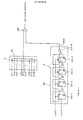
- Fig. 6 is a schematic circuit diagram of a conventional zero string error detection circuit.
- 1P and 1N represent shift registers.
- Shift register 1P receives the positive side of bipolar data P, which arrives serially, and converts it to parallel data composed of a specific number of bits (8 for example).
- Shift register 1N receives the negative side of bipolar data N, which arrives serially, and converts it to parallel data composed of a specific number of bits (8 for example).
- Component 2 is a B8ZS code detector.
- a B8ZS code (000VB0VB where V is a code which indicates that the data does not conform to the coding rule and B is a code which indicates that the data conforms to the coding rule - for example, if the output of shift register 1P is 00010001 and the output of shift register 1N is 00001010, the B8ZS code is detected) from parallel outputs FF1 to FF8 and FF1′ to FF8′ from the shift registers, it issues a reset signal FRST to shift registers 1P and 1N to make the 1P and 1N outputs zero.
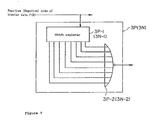
- Components 3P and 3N are 8-bit zero monitors. Eight-bit zero monitor 3P outputs a zero string error detection signal when it finds a string of eight zero bits in bipolar data P. Eight-bit zero monitor 3N outputs a zero string error detection signal when it finds a string of eight zero bits in bipolar data N. As indicated in Fig. 7, eight-bit zero monitors 3P and 3N are each provided with an eight-bit shift register 3P-1 (3N-1) and a NOR gate 3P-2 (3N-2) which receives the output of shift register 3P-1 (3N-1).
- the zero string detection signals are fed via an AND gate 4 (Fig. 6) to an alarm controller which is not indicated.
- the alarm controller detects zero string detection signals a specific number of times in succession, it sends an alarm to the transmitting end or other components.
- Component 5 is an OR gate for extracting output data. It receives the sixth outputs FF6 and FF6′ of shift registers 1P and 1N and outputs their OR as serial data.
- B8ZS code detector 2 When B8ZS code detector 2 detects a B8ZS in outputs from shift registers 1P and 1N in the above configuration, it issues a reset signal FRST to shift registers 1P and 1N to make the outputs of shift registers 1P and 1N zero. As a consequence, the B8ZS code is restored to eight zero bits.
- eight-bit zero monitors 3P and 3N issue zero string error detection signals, respectively. If the zero string error detection signals are issued a number of times in succession, the alarm controller issues an alarm to the transmitting end.
- Zero string error detection systems where a B6ZS code is detected have similar configuration and functions.
- the above conventional zero string error detection circuit with a B8ZS code converter involves a problem that a large-scale gate circuit must be used because zero strings are detected both in bipolar data P and in bipolar data N.
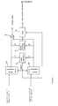
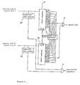
- An embodiment of the present invention can alleviate the above problem. It can provide a zero string error detection circuit of a relatively small gate size, making the shift register in the B8ZS or B6ZS code converter serve also to monitor strings of zeros.
- components 1P and 1N are respective shift registers which receive the positive side of bipolar data P and the negative side of bipolar data N respectively, which data arrives serially and is converted to parallel data of n bits (where n is a natural number).
- Component 2 is a code detector which, upon receiving a specific code from parallel outputs of shift registers 1P and 1N, issues a reset signal FRST to shift registers 1P and 1N to make the outputs of shift registers 1P and 1N zero.
- Component 3 is a zero string monitor which issues a zero string error detection signal when the parallel outputs of shift registers 1P and 1N become zero.
- Component 6 is a gate which, upon receiving a reset signal FRST from code detector 2, inhibits zero string monitor 3 from issuing a zero string error detection signal during a specific period.
- Component 5 is an OR gate for extracting output data.
- code detector 2 When code detector 2 detects a specific code in the outputs of shift registers 1P and 1N in the above configuration, it issues a reset signal FRST to shift registers 1P and 1N to make the outputs of shift registers 1P and 1N zero. As a consequence, the specific code is returned to the original number of zero bits.
- gate 6 Upon receiving a reset signal from code detector 2, gate 6 inhibits zero string monitor 3 from issuing the zero string error detection signal during a specific period. During this period, no alarm is issued to the transmitting end even when a zero string is detected.
- zero string monitor 3 issues a zero string detection error signal. Since code detector 2 does not issue a reset signal FRST even when the zero string continues, the mask function of gate 6 is disabled. If the zero string error detection signal is issued a number of times in succession, an alarm or other information is issued to the transmitting end.
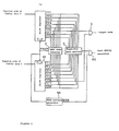
- Fig. 2 is a more detailed block circuit of diagram illustrating one embodiment of the invention.
- components 1P and 1N are shift registers; component 2 is a B8ZS code detector; component 3 is an eight-bit zero monitor.
- Shift registers 1P and 1N and B8ZS code detector 2 are the same as those of the conventional circuit shown in Fig. 6 and detailed explanation thereof is therefore omitted here.
- Eight-bit zero monitor 3 issues a zero string error detection signal when the parallel outputs FF1 to FF8 and FF1′ to FF8′ of shift registers 1P and 1N become zero.
- the zero monitor 3 is provided with a 16-input NOR gate 3A which receives parallel outputs FF1 to FF8 and FF1′ to FF8′ from shift registers 1P and 1N.
- gate 6B is provided to inhibit eight-bit zero monitor 3 from issuing a zero string error detection signal during a specified period (corresponding to eight clock cycles) when a reset signal FRST is output from B8ZS code detector 2.
- a mask pattern generator 6A When B8ZS code detector 2 issues a reset signal FRST, a mask pattern generator 6A outputs a mask signal MSK during the above period.
- the circuit of the mask pattern generator is a combination of a frequency divider fitted with four flip-flops 6A-1, 6A-2, 6A-3 and 6A-4 and an inverter 6A-5.
- Figs. 4(a) to (e) show the waveforms of the clock input to mask pattern generator 6A and other signals involved in its operation, from which the operation of the mask pattern generator will be clear.
- component 5 is an OR gate for extracting output data from sixth outputs FF6 and FF6′ of shift registers 1P and 1N.
- B8ZS code detector 2 When B8ZS code detector 2 detects a B8ZS code in the outputs of shift registers 1P and 1N in the above configuration, it issues a reset signal FRST to shift registers 1P and 1N to make the output of shift registers 1P and 1N zero. As a consequence, the B8ZS code is restored to eight zero bits.
- mask pattern generator 6A issues a mask signal MSK to AND gate 6B over a period of eight clock cycles. This inhibits eight-bit zero monitor 3 from outputting the zero string error detection signal. Therefore, an alarm or other information indicating the detection of a zero string is not issued to the transmitting end.
- eight-bit zero monitor 3 issues a zero string error detection signal.
- B8ZS code detector 2 does not issue a reset signal FRST even when the zero string continues. Therefore, the mask function of gate 6 (Fig. 1), containing mask pattern generator 6a (Fig. 2), is disabled. If the zero string error detection signal is issued a number of times in succession, an alarm controller (not shown) which has received those detection signals issues an alarm and other information to the transmitting end.
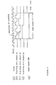
- Fig. 5 gives timing charts which apply to the above implementation example: (a) shows the waveform of clock CLK (synchronised with clock XCLK - Fig. 3) supplied to shift registers 1P and 1N; (b) and (c) show states 0 and 1 of positive and negative sides of the bipolar data (P and N); (d) shows the combination of positive and negative sides of the bipolar data (P and N); (e) to (l) show outputs FF1 to FF8 (FF1′ to FF8′) of shift register 1P (1N); (m) shows the waveform of the zero string error detection signal; (n) gives a timing chart for B8ZS code detection; (o) gives a timing chart for reset signal FRST output.
- FIG. 5 shows data which is obtained when the data P and data N shown in (b) and (c) respectively are combined. For simplification, this will be explained on the assumption that the data is serially input in shift registers 1P and 1N and output in parallel.
- shift registers FF1 to FF8 (FF1′ to FF8′) output "0" only.
- the mask signal itself has a width of only 7 bits, because the final output is obtained from the output FF6 (FF6′). More specifically, the code indicating all "0" is "000VB0VB", and when all zero is detected, output "0" has already been obtained from the output FF6 (FF6′).
- Gate size can be made much smaller than in the conventional circuit because shift registers 1P and 1N in the B8ZS code conversion circuit can also be used for eight-bit zero monitoring.
- embodiments of the invention can be applied to zero string error detection circuits which detect B6ZS code, for example.
- An embodiment of the present invention provides a zero string error detection circuit which detects a specified number of zeros occurring in succession in bipolar data.
- a relatively small gate size is achieved by making shift registers in a B8ZS or B6ZS code conversion circuit serve also for zero string monitoring.
- the zero string error detection circuit consists of a pair of shift registers which receive bipolar data arriving serially and convert it to parallel data composed of a specified number of bits, a code detector which, upon detecting a specific code from the parallel outputs of the shift registers, issues a reset signal to the shift registers to make the outputs of the shift registers zero, a zero string monitor which issues a zero string error detection signal when the outputs of the shift registers become zero, and a gate which inhibits the zero string monitor from issuing the zero string error detection signal during a specific period when the code detector issues a reset signal.
Landscapes
- Engineering & Computer Science (AREA)
- Computer Networks & Wireless Communication (AREA)
- Signal Processing (AREA)
- Physics & Mathematics (AREA)
- Spectroscopy & Molecular Physics (AREA)
- Detection And Prevention Of Errors In Transmission (AREA)
- Dc Digital Transmission (AREA)
- Error Detection And Correction (AREA)
Applications Claiming Priority (2)
| Application Number | Priority Date | Filing Date | Title |
|---|---|---|---|
| JP230703/88 | 1988-09-14 | ||
| JP63230703A JPH0710047B2 (ja) | 1988-09-14 | 1988-09-14 | 零連誤り検出回路 |
Publications (3)
| Publication Number | Publication Date |
|---|---|
| EP0359265A2 true EP0359265A2 (de) | 1990-03-21 |
| EP0359265A3 EP0359265A3 (de) | 1991-10-16 |
| EP0359265B1 EP0359265B1 (de) | 1995-06-07 |
Family
ID=16911993
Family Applications (1)
| Application Number | Title | Priority Date | Filing Date |
|---|---|---|---|
| EP89117042A Expired - Lifetime EP0359265B1 (de) | 1988-09-14 | 1989-09-14 | Detektoranordnung für Nullbitmuster-Fehler |
Country Status (4)
| Country | Link |
|---|---|
| US (1) | US5119380A (de) |
| EP (1) | EP0359265B1 (de) |
| JP (1) | JPH0710047B2 (de) |
| CA (1) | CA1324218C (de) |
Families Citing this family (4)
| Publication number | Priority date | Publication date | Assignee | Title |
|---|---|---|---|---|
| JP2960752B2 (ja) * | 1990-06-07 | 1999-10-12 | シャープ株式会社 | 半導体記憶装置 |
| US5343482A (en) * | 1991-07-16 | 1994-08-30 | Pmc-Sierra, Inc. | Method and apparatus for detecting pulse density violations in T1 transmission |
| US5555438A (en) * | 1991-07-24 | 1996-09-10 | Allen-Bradley Company, Inc. | Method for synchronously transferring serial data to and from an input/output (I/O) module with true and complement error detection coding |
| ATE298476T1 (de) * | 2003-04-11 | 2005-07-15 | Cit Alcatel | Störungsfreie umschaltung zwischen zwei redundanten pfade |
Family Cites Families (2)
| Publication number | Priority date | Publication date | Assignee | Title |
|---|---|---|---|---|
| JPS58161554A (ja) * | 1982-03-19 | 1983-09-26 | Hitachi Ltd | パルス信号伝送システム |
| US4757499A (en) * | 1986-12-22 | 1988-07-12 | Gte Communication Systems Corporation | Method for zero byte time slot interchange |
-
1988
- 1988-09-14 JP JP63230703A patent/JPH0710047B2/ja not_active Expired - Lifetime
-
1989
- 1989-09-13 CA CA000611168A patent/CA1324218C/en not_active Expired - Fee Related
- 1989-09-14 US US07/408,080 patent/US5119380A/en not_active Expired - Fee Related
- 1989-09-14 EP EP89117042A patent/EP0359265B1/de not_active Expired - Lifetime
Also Published As
| Publication number | Publication date |
|---|---|
| EP0359265B1 (de) | 1995-06-07 |
| CA1324218C (en) | 1993-11-09 |
| EP0359265A3 (de) | 1991-10-16 |
| JPH0279514A (ja) | 1990-03-20 |
| US5119380A (en) | 1992-06-02 |
| JPH0710047B2 (ja) | 1995-02-01 |
Similar Documents
| Publication | Publication Date | Title |
|---|---|---|
| KR0161511B1 (ko) | 데이타 워드 송신장치 및 수신장치 | |
| US6393082B1 (en) | Signal synchronism detecting circuit | |
| JPH02172327A (ja) | 符号化方法及び符号化装置 | |
| EP0276641A2 (de) | Datenkodierungsschnittstelle | |
| US5148453A (en) | Parallel sync detection | |
| JPS5813056B2 (ja) | 多重化パルス伝送システムにおける正確なフレ−ム化を維持する方法 | |
| EP0359265A2 (de) | Detektoranordnung für Nullbitmuster-Fehler | |
| US4009353A (en) | Analog signal detection | |
| EP0549247A1 (de) | Synchronisiersignaldetektor | |
| JP3498771B2 (ja) | 変調装置および方法 | |
| JPS63196130A (ja) | 信号検出方式 | |
| JPS642306B2 (de) | ||
| JP3246044B2 (ja) | 固定パターンのエラー測定装置 | |
| JP2826162B2 (ja) | 信号符号化方式および信号変換装置 | |
| RU2220502C2 (ru) | Преобразователь последовательного двоичного кода в параллельно-последовательный код | |
| JPS62122434A (ja) | フレ−ム信号同期検出回路 | |
| JPS62104333A (ja) | 交番信号監視回路 | |
| JP2555582B2 (ja) | Cmi符号誤り検出回路 | |
| EP0724207A2 (de) | Auf dem Verhältnis von Perioden des Haupt- und Untertaktes basierte Störungserkennung in einem Taktsignal | |
| JPH0134491B2 (de) | ||
| CA1285074C (en) | Data error detection circuit | |
| JPS61167244A (ja) | 通信制御装置 | |
| JPH0981367A (ja) | パターン検出回路 | |
| JPH0616635B2 (ja) | 誤りパルス検出回路 | |
| JPH0253326A (ja) | Hdb−3デコーダ符号則誤検出回路 |
Legal Events
| Date | Code | Title | Description |
|---|---|---|---|
| PUAI | Public reference made under article 153(3) epc to a published international application that has entered the european phase |
Free format text: ORIGINAL CODE: 0009012 |
|
| AK | Designated contracting states |
Kind code of ref document: A2 Designated state(s): DE FR GB |
|
| PUAL | Search report despatched |
Free format text: ORIGINAL CODE: 0009013 |
|
| AK | Designated contracting states |
Kind code of ref document: A3 Designated state(s): DE FR GB |
|
| 17P | Request for examination filed |
Effective date: 19911211 |
|
| 17Q | First examination report despatched |
Effective date: 19931123 |
|
| GRAA | (expected) grant |
Free format text: ORIGINAL CODE: 0009210 |
|
| AK | Designated contracting states |
Kind code of ref document: B1 Designated state(s): GB |
|
| PGFP | Annual fee paid to national office [announced via postgrant information from national office to epo] |
Ref country code: GB Payment date: 19950707 Year of fee payment: 7 |
|
| EN | Fr: translation not filed | ||
| PLBE | No opposition filed within time limit |
Free format text: ORIGINAL CODE: 0009261 |
|
| STAA | Information on the status of an ep patent application or granted ep patent |
Free format text: STATUS: NO OPPOSITION FILED WITHIN TIME LIMIT |
|
| 26N | No opposition filed | ||
| PG25 | Lapsed in a contracting state [announced via postgrant information from national office to epo] |
Ref country code: GB Effective date: 19960914 |
|
| GBPC | Gb: european patent ceased through non-payment of renewal fee |
Effective date: 19960914 |