EP0356986B1 - Pufferschaltung für logische Pegelumsetzung - Google Patents
Pufferschaltung für logische Pegelumsetzung Download PDFInfo
- Publication number
- EP0356986B1 EP0356986B1 EP89115900A EP89115900A EP0356986B1 EP 0356986 B1 EP0356986 B1 EP 0356986B1 EP 89115900 A EP89115900 A EP 89115900A EP 89115900 A EP89115900 A EP 89115900A EP 0356986 B1 EP0356986 B1 EP 0356986B1
- Authority
- EP
- European Patent Office
- Prior art keywords
- fet
- circuit
- voltage
- source
- field effect
- Prior art date
- Legal status (The legal status is an assumption and is not a legal conclusion. Google has not performed a legal analysis and makes no representation as to the accuracy of the status listed.)
- Expired - Lifetime
Links
Images


Classifications
-
- H—ELECTRICITY
- H03—ELECTRONIC CIRCUITRY
- H03K—PULSE TECHNIQUE
- H03K19/00—Logic circuits, i.e. having at least two inputs acting on one output; Inverting circuits
-
- H—ELECTRICITY
- H03—ELECTRONIC CIRCUITRY
- H03K—PULSE TECHNIQUE
- H03K19/00—Logic circuits, i.e. having at least two inputs acting on one output; Inverting circuits
- H03K19/0175—Coupling arrangements; Interface arrangements
- H03K19/0185—Coupling arrangements; Interface arrangements using field effect transistors only
- H03K19/018507—Interface arrangements
- H03K19/018535—Interface arrangements of Schottky barrier type [MESFET]
-
- H—ELECTRICITY
- H03—ELECTRONIC CIRCUITRY
- H03K—PULSE TECHNIQUE
- H03K19/00—Logic circuits, i.e. having at least two inputs acting on one output; Inverting circuits
- H03K19/003—Modifications for increasing the reliability for protection
- H03K19/00369—Modifications for compensating variations of temperature, supply voltage or other physical parameters
- H03K19/00384—Modifications for compensating variations of temperature, supply voltage or other physical parameters in field effect transistor circuits
-
- H—ELECTRICITY
- H03—ELECTRONIC CIRCUITRY
- H03K—PULSE TECHNIQUE
- H03K19/00—Logic circuits, i.e. having at least two inputs acting on one output; Inverting circuits
- H03K19/01—Modifications for accelerating switching
- H03K19/017—Modifications for accelerating switching in field-effect transistor circuits
- H03K19/01707—Modifications for accelerating switching in field-effect transistor circuits in asynchronous circuits
Definitions
- the present invention generally relates to buffer circuits, and more particularly to an input buffer circuit for converting a logic level of an input signal having an ECL (emitter-coupled-logic) level to a signal having a logic level suitable for use in a compound semiconductor integrated circuit.
- ECL emitter-coupled-logic
- bipolar ECL devices there are various semiconductor devices such as bipolar ECL devices, n-MOS (metal-oxide-semiconductor) devices, GaAs MESFET (gallium arsenide metal-semiconductor field effect transistor) devices, HEMT (high electron mobility transistor) devices and the like that are used in high speed logic integrated circuits.
- semiconductor devices such as bipolar ECL devices, n-MOS (metal-oxide-semiconductor) devices, GaAs MESFET (gallium arsenide metal-semiconductor field effect transistor) devices, HEMT (high electron mobility transistor) devices and the like that are used in high speed logic integrated circuits.
- silicon-based bipolar ECL devices are used most commonly.
- the logic level (voltage level) used in the silicon-based ECL device called ECL level is different from the logic level used in the compound semiconductor devices such as GaAs MESFET or HEMT. Therefore, there is a need to achieve a compatibility between the logic levels when devices of different type are used in a same system.
- an input/output buffer circuit is needed for achieving compatibility between the ECL device and other devices.
- Such an input/output buffer circuit is required to have a characteristic which is stable against the variation of the characteristic of the semiconductor devices used therein.
- a DCFL (direct coupled FET logic) device comprising an enhancement type FET and a depleiton type FET acting as a load of the enhancement type FET is particularly preferred from the view point of integration density, simple construction, small size, low power consumption, high operational speed and the like.
- the DCFL device is expected to play a major role in the logic gates of the future LSI (large scale integrated circuit) or VLSI (very large scale integrated circuit) devices.
- the first type of the prior art input buffer circuit uses two depletion type FETs and an inverter circuit in combination for producing a signal to be supplied to the following circuit which may be the DCFL device.
- the buffer circuit represented by a circuit 1 comprises a level shift circuit 2 and an inverter 3.
- the level shift circuit 2 comprises a pair of depleiton type FETs 4 and 5 connected in series, in which a source of the FET 4 is connected to a drain of the FET 5, a gate and a source of the FET 5 are connected each other, and a drain of the FET 4 is connected to the ground.
- the source of the FET 5 is further connected to a constant voltage source supplying a source voltage of - 3.6 volts.
- the inverter 3 comprises a depletion type FET 6 and an enhancement type FET 7 connected in series, wherein a source of the FET 6 is connected to a drain of the FET 7, a drain of the FET 6 is connected to the ground, and a source of the FET 7 is connected to a constant voltage source supplying a source voltage of - 2 volts. Further, the source of the FET 4 is connected to a gate of the FET 7.
- the level shift circuit 2 shifts the level of an input signal having the ECL level applied to a gate of the FET 4 and a signal having a level adapted to the following circuit is produced after inversion in the inverter 3.
- this circuit 1 one can change the amount of shift by choosing a gate width of the FETs 4 and 5. Further, one can obtain a buffering operation by setting the gate width of the FETs 6 and 7 properly so that the current flowing through these FETs is increased.
- This prior art buffer circuit has the following problems.
- the level shift circuit 2 is constructed by two FETs 4 and 5, there appears a change in the transfer characteristic of the buffer circuit 1 when the threshold voltage of the FETs 4 and 5 is varied.
- the threshold voltage of the FETs 4 and 5 is varied in the circuit of FIG.1 where the source of the FET 4 is connected to the source voltage of - 3.6 volts via the FET 5 having the gate and the source connected and acting as a constant current source, a voltage V SG appearing across the source and gate of the FET 4 is changed.
- the threshold voltage of the FET 6 is varied, the operational characteristic of the inverter 3 is also changed.
- the variation of the threshold voltage is relatively common in the current compound semiconductor FETs. Such a variation is caused also as a result of the side gate effect which will be described later.
- FIG.2 shows such a change of the transfer characteristic of the buffer circuit 1.
- the abscissa represents an input voltage V in applied to the gate of the FET 4 and the ordinate represents an output voltage V out obtained from the drain of the FET 7 for a case in which the threshold voltage of the enhancement type FET 7, designated as V TE , is fixed at 0.25 volts and the threshold voltage of the depletion type FETs 4, 5 and 6, designated as V TD , is changed from - 0.3 volts to - 0.8 volts with an interval of 0.1 volts.
- the buffer circuit 1 has a transfer characteristic which is extremely sensitive to the variation in the threshold voltage of the depletion type FET 7.
- the FET 4 is a HEMT device.
- the FET 4 is constructed on a GaAs substrate 11 and comprises a GaAs epitaxial layer 12 having a predetermined layered structure grown epitaxially on the GaAs substrate 11, an AlGaAs (aluminium gallium arsenide) epitaxial layer 12′ further grown epitaxially on the layer 12, a source electrode 13, a gate electrode 14 and a drain electrode 15 each provided on the layer 12′, an isolation structure 16 formed in the layer 12, and an electrode 17 also on the layer 12′ for application of the voltage of - 3.6 volts.
- the electrical field created by the electrode 17 extends beyond the isolation structure 16 to a region under the gate electrode 14 particularly when the magnitude of the voltage applied to the electrode 17 is large such as - 3.6 volts, and responsive thereto, the electrical potential in the region under the gate electrode 14 is changed which in turn causes a modification of the threshold level V th of the FET 4.
- Such an effect is known as the side gate effect. It is said that such a change of the electrical potential is caused by electrons trapped in the surface state which in turn is developed at a boundary between the GaAs substrate 11 and the epitaxial layer 12′.
- the side gate effect can be observed most clearly in a plot of a square root source-drain current versus source-drain voltage shown in FIG.4.
- the current flowing through the FET 4 with a so-called square root-law extends generally straight with the source-drain voltage V SG and has an intercept at the abscissa indicative of the threshold voltage V th of the FET.
- the characteristic curve is shifted as shown in the drawing, and together with this, the threshold voltage V th is changed to V th + ⁇ V.
- the operational characteristic of the buffer circuit 1 is significantly effected.
- This side gate effect arises as a result of use of large source voltage (- 3.6 volts) as already noted.
- the side gate effect is of course reduced.
- such a measure is contradictory to the requirement to increase the integration density and hence the operational speed of the device.
- the side gate effect has been a serious problem in the integrated circuit of compound semiconductor devices such as HEMT.
- the buffer circuit is represented by a reference numeral 21 and comprises an inverter 22 for inverting an input signal supplied thereto and a level shift (level conversion) circuit 23 for shifting an output level of the inverter 22.
- the inverter 22 comprises depletion type FETs 24 - 26 and enhancement type FETs 27 and 28 wherein each of the FETs 24 - 26 has a gate and drain connected each other and all the FETs 24 - 27 are connected in series.
- the FET 27 has a source connected to a gate of the FET 28 and also a drain connected to a drain of the FET 28.
- FETs 27 and 28 form a Darlington's pair.
- the level shift circuit 23, comprises a series connection of an enhancement type FET 29 and a depletion type FET 30, wherein the FET 30 has a source and a gate connected to each other.
- the drain of the FET 24 is connected to the ground, a drain of the FET 29 also connected to the ground, a source of the FET 28 connected to a constant voltage source supplying a source voltage of - 2 volt, and the source of the FET 30 connected to the constant voltage source.
- the inversion of the inverter 22 is basically determined by a sum of the threshold voltage of the FETs 27 and 28.
- FIG.6(A) shows a depletion type FET 31 having a gate and source connected each other.
- the FET shows a voltage versus current characteristic shown in FIG.6(B) wherein the ordinate represents a source-drain current I SD and the abscissa represents a source-drain voltage V SD .
- FIG.6(B) there is an extensive saturated region where the current I SD remains substantially the same with increase of the source-drain voltage V SD .
- the threshold voltage in the FET 31 connected as shown in FIG.6(A) the current level in the saturated region is changed as shown in FIG.6(B).
- This connection of the FET 31 is similar to the connection of the FET 5 described with reference to FIG.1.
- V th assumes a negative value and V GS and V DS assume an identical voltage level.
- the left hand side of the inequality is always larger than the term in the right hand side.
- I SD stands for the source-drain current of the FET 32 and K is a constant.
- FIG.7(B) shows the characteristic defined by Eq.(2) graphically. It can be seen that the variation of the current I SD caused by the variation of the threshold voltage of the FET 32 is generally very small.
- FIG.8 shows a result of simulation undertaken for the buffer circuit 21. Note that FIG.8 shows the transfer characteristic. In the simulation, it was assumed that a threshold voltage V TE for the FETs 27, 28 and 29 is fixed at 0.25 volts and a threshold voltage V TD for the FETs 24 - 26 and 30 is changed from - 0.3 volts to - 0.8 volts with an 0.1 volt interval. As is clear from FIG.8, the buffer circuit 21 is stable against change in the threshold voltage of the depletion FET. Further, the circuit is less sensitive to the side gate effect as the use of the source voltage of - 3.6 volts which has been the cause of the side gate effect in the circuit of FIG.1 is now eliminated by changing the source voltage to - 2 volts.
- FIG.9 shows the transfer characteristic for the case of the circuit 21 wherein the threshold voltage V TD of the FETs 24 - 26 and 30 are fixed at - 0.5 volts while the threshold voltage V TE of the FETs 27, 28 and 30 is changed from 0.15 volts to 0.3 volts with an interval of 0.05 volts.
- the transfer characteristic of the buffer circuit 21 changes significantly with the variation of the threshold voltage.
- the voltage level appearing at a node A of FIG.5 is indefinite and the circuit 21 tends to exhibit unstability in the operation. This leads to a poor transient characteristic.
- the circuit 33 comprises a level shift part 34, another level shift part 35, differential part 36 and a reference part 37, in which the level shift parts 34 and 35 have a similar circuit construction as the level shift circuit 2 used in the buffer circuit of FIG.1.
- the level shift part 34 comprises a pair of depletion type FETs 38 and 39 while the level shift part 35 comprises a pair of depletion type FETs 40 and 41.
- an input signal to the buffer circuit 33 is applied to a gate of the FET 38 and a reference voltage produced by the reference part 37 is applied to a gate of the FET 40.
- the differential part 36 comprises a pair of depletion type FETs 42 and 43, a pair of enhancement type FETs 44 and 45 respectively connected to the FETs 42 and 43 in series, and a depletion type FET 46 having a source and gate connected to each other, wherein the FET 44 and the FET 45 have respective sources connected in common to a drain of the FET 46.
- the FET 44 receives a signal subjected to level shifting from the level shift part 34 and the FET 45 receives a reference yoltage also subjected to level shifting from the reference part 37 via the level shift part 35. This reference voltage supplied to the FET 45 is used as the logic threshold in the differential part 36.
- the reference part 37 comprises a depletion type FETs 47 and 48 in which each of the FETs 47 and 48 have respective gates and sources which are connected each other. Further, a source voltage of - 3.6 volts is supplied to the level shift parts 34 and 35 as well as to the differential part 36. The reference part 37 on the other hand receives a source voltage of - 2 volts.
- this circuit has a problem in that the variation of the threshold voltage of the FETs causes a significant change in the transfer characteristic similarly to the case of the level shift circuit 2 in the buffer circuit of FIG.1. Further, there is another problem in that the reference voltage produced by the reference part 37 is changed responsive to the variation in the threshold voltage of the FETs 47 and 48.
- the circuit 33 suffers from the side gate effect as a result of the use of the source voltage which is set to - 3.6 volts. According to the experiment, the buffer circuit 33 is more sensitive to the side gate effect than the buffer circuit 1.
- EP-A-0 313 810 concerning state of the art according to article 54(3) EPC discloses a source-follower emitter-coupled-logic receiver circuit for interfacing between small emitter-coupled-logic circuit voltage levels and larger field effect transistor circuits voltage level.
- the circuit comprises an input terminal to which an input signal is applied, a first voltage source, namely the positive supply voltage, a second voltage source, namely ground, first resistance means formed by a first transistor; the source of which is coupled to the positive supply voltage, a first enhancement type FET provided between the drain of the first transistor and ground and the gate of which is connected to the input terminal.
- a second resistance means formed by a second transistor and a second enhancement type FET is provided, wherein the gate of the second enhancement type FET is connected to the input terminal and the source is connected to the drain of the first enhancement FET.
- the second transistor is provided between the positive supply voltage and the drain of the second enhancement type FET.
- the gate of the second transistor is connected to a predetermined voltage.
- a further prior art document according to article 54(3) is EP-A-0 292 713.
- a low voltage swing CMOS receiver or buffer circuit is disclosed.
- the circuit comprises a first series circuit having first and second P channel transistors (second and first enhancement FETs), and a first N channel transistor (second resistance means) and a second series circuit having second and third N channel transistors (first resistance means) with the third N channel transistor connected as a diode.
- the first series circuit with an output terminal is connected between a voltage supply terminal and a point of reference potential, such as ground, and the second series circuit is connected from the common point between the first and second P channel and ground.
- An input terminal is connected to the control electrodes of the first and second P channel transistors and of the first N channel transistor, as well as to the control electrode of the third N channel transistor.
- EP-A-0 154 337 discloses a transistor circuit with hyteresis operation for converting a logical level of an input signal.
- the circuit includes a level change detector circuit and a threshold selector circuit.
- the level change detector circuit is formed with a P channel MOS transistor (second resistance means) and an first N channel MOS transistor (second enhancement FET).
- the source of the P channel transistor is connected to a positive power supply terminal.
- the gate of this transistor receives an input signal, and the drain thereof provides an output signal which is anti-phasic to the input signal.
- the drain and the gate of the N channel transistor are connected to the drain and gate of the P channel transistor, respectively.
- the threshold selector circuit is formed with second and third N channel MOS transistors (first enhancement FET, first resistance means).
- the drain of second transistor is connected to the source of first N channel transistor, and the gate of second transistor receives the input signal.
- the source of second transistor is connected to a circuit-ground.
- the drain of third transistor is connected to the power supply terminal.
- the gate of third transistor receives the output signal, and the source thereof is connected to the drain of second transistor.
- Another and more specific object of the present invention is to provide an input buffer circuit wherein the side gate effect causing variation in the threshold voltage of field effect transistors is successfully eliminated.
- Another object of the present invention is to provide an input buffer circuit wherein the effect of variation in the threshold voltage of field effect transistors on the transfer characteristic of the input buffer circuit is minimized.
- Another object of the present invention is to provide an input buffer circuit having an excellent transient characteristic.
- Another object of the present invention is to provide an input buffer circuit having a stable transient characteristic.
- Another object of the present invention is to provide an input buffer circuit having a large operational margin.
- Another object of the present invention is to provide an input buffer circuit which reduces the load of a driving circuit in a preceding stage for driving the input buffer circuit.
- Another object of the present invention is to provide a buffer circuit comprising an inversion circuit and a level shift circuit, wherein said inversion circuit comprises a first voltage source for supplying a first predetermined voltage, a second voltage source for supplying a second predetermined voltage which is lower than said first predetermined voltage, a first load resistance having a first end connected to the first voltage source, a first enhancement type field effect transistor having a source connected to a second end of the first load resistance and a drain connected to said second voltage source, said first enhancement type field effect transistor having a gate connected to an input terminal of the buffer circuit, a second load resistance having a first end connected to the first voltage source, a second enhancement type field effect transistor having a drain connected to a second end of the second load resistance, said second enhancement type field effect transistor having a source connected to the drain of said first enhancement type field effect transistor and a gate connected to the input terminal of the buffer circuit, and wherein said level shift circuit is connected to the drain of the second enhancement type field effect transistor.
- transfer characteristic of the buffer circuit does not change substantially even when there is a variation of the threshold voltage in the field effect transistors as the voltage drop caused across the source and drain of the first enhancement type field effect transistor compensates the variation of the threshold voltage either in the first and second enhancement type field effect transistors.
- the buffer circuit of the present invention successfully eliminates the side gate effect by using the source voltage having a small magnitude.
- the buffer circuit has an excellent transient characteristic because of the elimination of Darlington's connection for the first and second enhancement type field effect transistors.
- a third depletion type field effect transistor having its gate connected to its source such that a drain thereof is connected to an input terminal of the buffer circuit and the source thereof is connected to the gate of the first enhancement type field effect transistor, excessive input current to the first enhancement type field effect transistor is suppressed and the low level state appearing in the transfer characteristic is shifted lower. Accordingly, the load viewed from succeeding circuits is reduced and the operational margin of the buffer circuit is increased. Further, by providing a capacitor across the drain and source of the third depletion type field effect transistor, an excellent transient characteristic can be achieved.
- the input buffer circuit represented as a circuit 51 comprises an inverter 52 and a level shift circuit identically constructed to the level shift circuit 23 already described with reference to FIG.5.
- the level shift circuit will be designated as circuit 23 and the description thereof will not be repeated.
- the inverter comprises depletion type field effect transistors 53 - 58 and a pair of enhancement type field effect transistors 59 and 60, wherein each of the transistors 53 - 58 has a gate connected to a drain of the same transistor.
- the FETs 53- 58 as well as the FETs 59 and 60 are assumed to be the HEMT device. However, the FETs are not limited as such but other high speed devices such as GaAs MESFET can also be used.
- the FETs 53 - 55 are connected in series and the drain of the FET 53 is connected to the ground while a source of the the transistor 55 is connected to a drain of the enhancement type FET 59.
- This FET 59 in turn has a source connected to a voltage source supplying a source voltage of - 2 volts.
- the FETs 53 - 55 and the FET 59 are connected in series between the ground and the voltage source.
- the FET 59 has a gate connected to an input terminal 61 of the buffer circuit 51 and receives an input logic signal having the ECL level from the input terminal 61.
- the FETs 56 - 58 are connected in series wherein the drain of the FET 56 is connected to the ground and a source of the FET 58 is connected to a drain of the enhancement type FET 60.
- the FET 60 has a source connected to the drain of the FET 59 and a gate connected to the input terminal 61 commonly with the gate of the FET 59.
- the inverter 52 thus constructed supplies an output signal from the drain of the FET 60 to the level shift circuit 23 for level shifting, and a signal thus subjected to level shifting is supplied to the following stage (not shown) through an output terminal 62.
- a part of the circuit 51 including the FETs 53 - 55 designated by a reference numeral 71 and a part of the circuit including the FETs 56 - 58 designated by a reference numeral 72 respectively act as load to the FETs 59 and 60 whereby each of them has a construction to maintain the circuit characteristic unchanged against the variation of the threshold voltage of the FETs 53 - 55 or the FETs 56 - 58.
- Another part of the inverter 52 including the FETs 59 and 60 and designated by a reference numeral 73 is an essential part of the present invention and has a connection designed such that the variation of the threshold voltage in the FETs 59 and 60 does not cause change in the logic threshold of the inverter 52 as will be described later.
- loads 71 and 72 comprise three FETs connected in series as shown in FIG.11.
- the input buffer circuit 51 has another feature in that the side gate effect is minimized by setting the source voltage to - 2 volts.
- the FETs 53 - 55 in the circuit part 71 or the FETs 56 - 58 in the circuit part 72 has a connection in which the gate and drain are connected each other in each of the transistors.
- the FETs are operated in the linear region and the change of the operational characteristic of each of the FETs is minimized similarly to the FETs 24 - 26 shown in FIG.5.
- the operational principle of the FETs having such a connection is already described with reference to FIG.5 as well as FIGS.7(A) and (B) and will not be repeated.
- FIG.13 shows a voltage versus current characteristic of the FETs 53 - 58 wherein the ordinate represents a source-drain current I SD and the abscissa represents a source-drain voltage V SD .
- the transistors 53 - 58 connected as such operate in the linear region and the characteristic curve simulated for the actual FETs is stable against the variation of the threshold voltage.
- FIG.12 shows, for the purpose of comparison, a hypothetical case in which the FETs 53 - 58 are connected as shown in FIG.6(A).
- the FETs thus connected operate in the saturated region and a characteristic similar to FIG.6(B) is obtained.
- circuit part 73 is designed to minimize the change of transfer characteristic responsive to the variation of the enhancement type FETs 59 and 60 and constitutes the essential part of the present invention.
- the operational principle of the circuit part 73 will be described with reference to FIG.14 which shows the inverter 52 in a simplified form.
- the circuit part 71 and the circuit part 72 acting as the load to the FETs 59 and 60 will be represented as resisters R1 and R2.
- the current flowing through the resister R1 is designated as I1 and the current flowing through the resister R2 will be referred to as I2.
- the source voltage of - 2 volts supplied from the voltage source is replaced by the ground level and the ground level voltage applied to the resisters R1 and R2 is replaced by a voltage of 2 volts.
- FIG.15 shows the voltage versus current characteristic of the enhancement type FET 59
- FIG.16 shows the voltage versus current characteristic of the enhancement type FET 60 following the FET 59.
- the characteristic curve of the FET 59 is crossed with a load line in the unsaturated region while the characteristic curve of the FET 60 is crossed with the load line in the saturated region.
- I1 (2 - V s )/R (3)
- I1+I2 2K[(V in -V T )-1/2V s ]V s (4)
- I2 (2 - V out )/R (5)
- I2 K[(V in -V s ) - V T ]2 (6)
- V in stands for an input voltage
- V out stands for an output voltage of the inverter 52
- V T stands for the threshold voltage of the FETs 59 and 60
- K is a constant.
- the current I1+I2 given by Eq.(4) is determined by the characteristic of the FET 59 as the currents I1 and I2 both flows through the FET 59.
- Eq.(4) is for the operation in the unsaturated region.
- the current I2 on the other hand flows explicitly through the FET 60 and therefore is determined by the operational characteristic of the FET 60. It is assumed that the FET 60 operates in the saturated region as can be seen from Eq.(6).
- the overdrive of the FET 59 is increased which results in the decrease of the drain-source current flowing through the FET 59.
- the drain voltage of the FET 59 as well as the source voltage of the FET 60 is increased and the threshold characteristic of the inverter viewed form its input side does not change virtually.
- FIGS.17 and 18 show result of simulation undertaken for the input buffer circuit 51.
- FIG.17 showing the transfer characteristic of the buffer circuit 51 for a case in which the threshold voltage V TD of the FETs 53 - 58 and as well as the FET 30 is changed from - 0.3 volts to - 0.8 volts with an interval of 0.1 volt while fixing the threshold voltage V TE of the FETs 59, 60 and 29 at 0.25 volts, it is clear that the change of the transfer characteristic with the variation in the threshold voltage is minimum similarly to the case of FIG.8.
- FIG.18 shows the transfer characteristic of the buffer circuit for a case in which the threshold voltage V TE of the enhancement type FETs 59, 60 and 20 is changed from 0.15 Volts to 0.3 volts with an interval of 0.05 volts while fixing the threshold voltage of the FETs 53 - 58 as well as the FET 30 at - 0.5 volts. From FIG.18, it can be seen that the transfer characteristic shifts to the right by about 0.05 volts responsive to a variation of the threshold voltage V TE amounting 0.05 volts.
- the input buffer circuit 51 has the transfer characteristic which changes substantially less responsive to the same variation of the threshold voltage of the enhancement type FETs 59, 60 and 30.
- the threshold voltage change of ⁇ V causes the shift of the characteristic curve which amounts as much as 2 ⁇ V.
- a same change of the threshold voltage causes the shift amounting only ⁇ V.
- change of the threshold voltage by ⁇ V in a circuit comprising a pair of FETs connected in series causes a change of output voltage of 2 ⁇ V.
- the input buffer circuit 51 uses the source voltage set to - 2 volts and the variation of the threshold voltage caused by the side gate effect is suppressed. Further, the change of the transfer characteristic due to the variation of the threshold voltage of the depletion type FETs used in the circuit parts 71 and 72 can be successfully suppressed as already described with reference to FIG.17. Thus, the transfer characteristic of the input buffer circuit 51 is stable against the variation of the threshold voltage of both the enhancement type and depletion type FETs. Furthermore, there is an advantage in that the logic threshold level can be set to the desired level relatively easily as the logic level is set by the enhancement type FET.
- the input buffer circuit 51 described heretofore is preferred from the reasons set forth before.
- This circuit 51 is turned out to have a problem in that the low level in the transfer characteristic is raised when a high level ECL signal having a level of - 0.8 volts is applied to the input terminal 61.
- a high level ECL signal having a level of - 0.8 volts is applied to the input terminal 61.
- a voltage of 1.2 volt appears across the gate and source of the FET 59 and a large current flows through the Schottky gate of the FET 59.
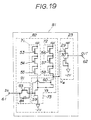
- FIG.19 shows an input buffer circuit 81 which constitutes the second embodiment of the present invention.
- these parts having identical construction to those corresponding parts in FIG.11 will be given identical reference numerals and the description thereof will be omitted.
- the input buffer circuit 81 comprises an inverter 82 and a level shift circuit constructed identically to the level shift circuit 23.
- the inverter 82 comprises the depletion type FETs 53 - 58, another depletion type FET 83, the enhancement type FETs 59 and 60 and a capacitor 84.
- the FETs 53 - 58 and the FETs 59 and 60 are connected similarly to the circuit 51 of FIG.11. Further, a same source voltage is used.
- the circuit 81 has a generally similar construction to the circuit 51 and operates similarly.
- the circuit 81 differs from the circuit 51 in that it has the depletion type FET 83 connected in series between the input terminal 61 and the gate of the FET 59.
- the FET 83 has a drain connected to the input terminal 61 and a source connected to the gate of the FET 59. Further, the FET has a gate connected to its source.
- the capacitor 84 is connected across the source and drain of the FET 83.
- the FET 83 and the capacitor 84 forms a circuit part 91 and the input buffer circuit 81 has a construction such that the circuit part 91 is added to the buffer circuit 51 of FIG.11.
- the FET 83 may be the HEMT device or GaAs MESFET device.
- the current supplied to the gate of the FET 59 is limited by the depletion type FET 83 connected to operate in the saturated region.
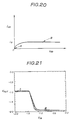
- the FET 83 acts as a constant current source and the current at the gate of the FET 59 does not exceed a level I0 corresponding to an operational point B shown in FIG.20 even when there is a large voltage applied across the source and drain through the input terminal 61.
- the FET 83 connected limits the current to the gate of the FET 59 and the unwanted rise of the low level state is successfully eliminated.
- FIG.21 shows the transfer characteristic of the input buffer circuit 81 having the FET 83 connected in series to the gate of the FET 59. As can be clearly seen from FIG.21, the level of the point B is definitely lower than that of the point B′ in FIG.17.
- FIG.22 shows such a response of the circuit 81 to a series of input signals having a rectangular waveform for a case in which the threshold voltage V TD is changed from - 0.3 volts to - 0.8 volts with an interval of 0.1 volts while fixing the threshold voltage V TE at 0.25 volts. It can be seen from the drawing that there appears a delay in response particularly when the threshold level of the depletion type FETs is changed.
- FIG.23 shows the transient response of the input buffer circuit 81 which is further provided with the capacitor 84.
- the response of the circuit is significantly improved.
- the capacitor 84 may be a diode applied with a reversed bias voltage.
- the operation of the circuit 81 will be described with reference to FIG.19.
- the ECL signal applied to the input terminal 61 has a level lower than the threshold level of the enhancement type FET 59
- the FET 59 is turned off and the voltage appearing at a node V M shown in FIG.19 is substantially zero.
- This voltage is shifted by the level shift circuit 23 and supplied to the output terminal 62 as an output signal of the input buffer circuit 81.
- the level shift circuit 23 By setting the level shift circuit 23 such that a voltage of about one volt is obtained as the output voltage in this state, compatibility with the DCFL device is achieved.
- the FET 59 When the input voltage is increased, the FET 59 is turned on and the voltage V s appears at the drain of the FET 59. In this state, the voltage appearing across the gate and source of the enhancement type FET 60 is represented as V in - V s and thus the FET 60 does not turn on yet. Thus, the voltage at the node V M is substantially zero and the output voltage of about one volt is obtained from the level shift circuit 23. The operation so far corresponds to a point A shown in FIG.20.
- both the FET 59 and the FET 60 are turned on and the node V M assumes a voltage level which is higher than the low level used in the DCFL device by an amount equal to the voltage across the FETs 59 and 60.
- This voltage at the node V M is then shifted by the level shift circuit 23 and is converted to the low level of the DCFL device. This operation is represented by the point B in FIG.21.
- the voltage applied to the FET 83 becomes zero and the transfer characteristic becomes identical to the case in which the FET 83 is not provided.
- voltage is applied across the gate and source of the FET 59 and current flows through the FET 59.
- the FET 83 is provided, the current flowing in to the gate of the FET 59 is limited as already described and the voltage is divided by the FET 83 and FET 59.
- the input buffer circuit of the present embodiment provides a transfer characteristic which is stabilized against variation of the FETs constituting the circuit and an improved and stable transient characteristic. Further, the low level state in the transfer characteristic is lowered and the operational margin of the circuit is extended. Furthermore, the load of circuits supplying the input signal to the buffer circuit is also reduced.
Claims (6)
- Eingangspuffer zum Umwandeln eines Logikpegels eines Eingangs-Logiksignals mit einem Inverter (52, 82), dem das Eingangs-Logiksignal zum Invertieren des Logikpegels zugeführt wird, wobei der Inverter (52, 82) umfaßt einen Eingangsanschluß (61), dem das Eingangssignal zugeführt wird, eine erste Spannungsquelle (Erde) zum Bereitstellen einer vorbestimmten ersten Spannung, eine zweite Spannungsquelle (-2V) zum Bereitstellen einer vorbestimmten zweiten Spannung mit einem gegenüber der vorbestimmten ersten Spannung Kleineren Pegel, wobei ein erster Widerstand (71) ein mit der ersten Spannungsquelle verbundenes erstes Ende aufweist, wobei ein erster Anreicherungs-Feldeffekt-Transistor (59) einen mit dem zweiten Ende des ersten Widerstands verbundenen Drain, eine mit der zweiten Spannungsquelle verbundene Source und ein mit dem Eingangsanschluß verbundenes Gate aufweist, wobei ein zweiter Widerstand (72) ein mit der ersten Spannungsquelle verbundenes erstes Ende hat, und wobei ein zweiter Anreicherungs-Feldeffekt-Transistor (60) einen mit dem zweiten Ende des zweiten Widerstands verbundenen Drain, eine mit dem Drain des ersten Anreicherungs-Feldeffekt-Transistors verbundene Source und ein mit dem Gate des ersten Anreicherungs-Feldeffekt-Transistors verbundenes Gate aufweist, wobei der erste und der zweite Widerstand (71, 72) eine Reihenschaltung von Verarmungs-Feldeffekt-Transistoren (53-54, 56-58) umfassen, worin jeder Verarmungs-Feldeffekt-Transistor eine mit dem Gate desselben Feldeffekt-Transistors verbundene Drain aufweist.
- Eingangspuffer nach Anspruch 1, dadurch gekennzeichnet, daß der erste als auch der zweite Widerstand (71, 72) drei Schottky-Gate-Feldeffekt-Transistoren (53-55, 56-58) umfaßt.
- Eingangspuffer nach Anspruch 1, dadurch gekennzeichnet, daß der Pegel der vorbestimmten zweiten Spannung um etwa 2 Volt kleiner ist als der Pegel der vorbestimmten ersten Spannung.
- Eingangspuffer nach Anspruch 1, desweiteren gekennzeichnet durch einen Strombegrenzer (91), der zwischen dem Eingangsanschluß (61) und dem Gate des ersten Anreicherungs-Feldeffekt-Transistor (59) angeordnet ist, zum Begrenzen eines diesen durchlaufenden Stroms auf einen vorbestimmten Strompegel.
- Eingangspuffer nach Anspruch 4, dadurch gekennzeichnet, daß der Strombegrenzer (91) einen Verarmungs-Feldeffekt-Transistor (83), der einen mit dem Eingangsanschluß (61) verbundenen Drain, eine mit dem Gate des ersten Anreicherungs-Feldeffekt-Transistors verbundene Source und ein mit der Source desselben Verarmungs-Feldeffekt-Transistors verbundenes Gate aufweist, und eine Kapazität (84) umfaßt, die mit dem Drain und der Source des Verarmungs-Feldeffekt-Transistors verbunden ist.
- Eingangspuffer nach Anspruch 1, dadurch gekennzeichnet, daß der Eingangspuffer desweiteren umfaßt eine Pegel-Umsetzschaltung (23), die zum Empfang eines Ausgangssignals des Inverters vorgesehen ist und dessen Pegel umsetzt, wobei die Pegel-Umsetzschaltung einen dritten Anreichetungs-Feldeffekt-Transistor (29) und einen Verarmungs-Feldeffekt-Transistor (30) aufweist, die in Reihe liegen, wobei der dritte Anreicherungs-Feldeffekt-Transistor einen mit der ersten Spannungsquelle verbundenen Drain, ein mit der Drain des zweiten Anreicherungs-Feldeffekt-Transistor (60) verbundenes Gate und eine mit der Drain des Verarmungs-Feldeffekt-Transistors verbundene Source aufweist, und daß der Verarmungs-Feldeffekt-Transistor eine Source und ein Gate hat, die gemeinsam mit der zweiten Spannungsquelle verbunden sind.
Applications Claiming Priority (2)
| Application Number | Priority Date | Filing Date | Title |
|---|---|---|---|
| JP216732/88 | 1988-08-30 | ||
| JP63216732A JPH0263319A (ja) | 1988-08-30 | 1988-08-30 | 入力バッファ |
Publications (3)
| Publication Number | Publication Date |
|---|---|
| EP0356986A2 EP0356986A2 (de) | 1990-03-07 |
| EP0356986A3 EP0356986A3 (en) | 1990-09-19 |
| EP0356986B1 true EP0356986B1 (de) | 1994-04-13 |
Family
ID=16693062
Family Applications (1)
| Application Number | Title | Priority Date | Filing Date |
|---|---|---|---|
| EP89115900A Expired - Lifetime EP0356986B1 (de) | 1988-08-30 | 1989-08-29 | Pufferschaltung für logische Pegelumsetzung |
Country Status (5)
| Country | Link |
|---|---|
| US (1) | US5051626A (de) |
| EP (1) | EP0356986B1 (de) |
| JP (1) | JPH0263319A (de) |
| KR (1) | KR920005359B1 (de) |
| DE (1) | DE68914548D1 (de) |
Families Citing this family (10)
| Publication number | Priority date | Publication date | Assignee | Title |
|---|---|---|---|---|
| DE69119643T2 (de) * | 1990-03-15 | 1996-09-26 | Fujitsu Ltd | Pufferschaltung zur logischen Pegelumsetzung |
| JPH0595267A (ja) * | 1991-10-02 | 1993-04-16 | Sumitomo Electric Ind Ltd | 半導体論理装置 |
| JP3365804B2 (ja) * | 1993-01-12 | 2003-01-14 | 株式会社日立製作所 | 通信回線駆動回路、及びインタフェース用lsi、並びに通信端末装置 |
| US5420527A (en) * | 1994-04-06 | 1995-05-30 | Itt Corporation | Temperature and supply insensitive TTL or CMOS to 0/-5 V translator |
| JPH08204536A (ja) * | 1995-01-20 | 1996-08-09 | Fujitsu Ltd | インタフェース回路及びレベル変換回路 |
| US6147540A (en) | 1998-08-31 | 2000-11-14 | Motorola Inc. | High voltage input buffer made by a low voltage process and having a self-adjusting trigger point |
| KR20030007299A (ko) * | 2002-12-04 | 2003-01-23 | (주) 바이탈인터내셔날 | 발광장치를 구비하는 가방 |
| US8154320B1 (en) * | 2009-03-24 | 2012-04-10 | Lockheed Martin Corporation | Voltage level shifter |
| CN111786642A (zh) * | 2020-07-10 | 2020-10-16 | 无锡英迪芯微电子科技股份有限公司 | 具有端口电压保护功能的推挽结构端口输出电路 |
| CN114070297A (zh) * | 2020-08-05 | 2022-02-18 | 圣邦微电子(北京)股份有限公司 | 微功耗的电平翻转电路及降低电路中瞬态电流的方法 |
Citations (3)
| Publication number | Priority date | Publication date | Assignee | Title |
|---|---|---|---|---|
| EP0154337A2 (de) * | 1984-03-06 | 1985-09-11 | Kabushiki Kaisha Toshiba | Transistorschaltung für Halbleitervorrichtung mit Hysterese-Verhalten und ihre Herstellungsverfahren |
| EP0292713A2 (de) * | 1987-05-26 | 1988-11-30 | International Business Machines Corporation | CMOS-Empfangsschaltung für niedrigen Spannungshub |
| EP0313810A2 (de) * | 1987-10-30 | 1989-05-03 | International Business Machines Corporation | Quellenfolger-Empfängerschaltung für ECL |
Family Cites Families (3)
| Publication number | Priority date | Publication date | Assignee | Title |
|---|---|---|---|---|
| JPS5550743A (en) * | 1978-10-11 | 1980-04-12 | Fujitsu Ltd | Level shift circuit |
| US4791322A (en) * | 1987-05-19 | 1988-12-13 | Gazelle Microcircuits, Inc. | TTL compatible input buffer |
| US4767951A (en) * | 1987-06-30 | 1988-08-30 | Hewlett-Packard Company | ECL to NMOS converter |
-
1988
- 1988-08-30 JP JP63216732A patent/JPH0263319A/ja active Pending
-
1989
- 1989-08-29 EP EP89115900A patent/EP0356986B1/de not_active Expired - Lifetime
- 1989-08-29 DE DE68914548T patent/DE68914548D1/de not_active Expired - Lifetime
- 1989-08-29 KR KR1019890012350A patent/KR920005359B1/ko not_active IP Right Cessation
-
1990
- 1990-11-09 US US07/610,461 patent/US5051626A/en not_active Expired - Fee Related
Patent Citations (3)
| Publication number | Priority date | Publication date | Assignee | Title |
|---|---|---|---|---|
| EP0154337A2 (de) * | 1984-03-06 | 1985-09-11 | Kabushiki Kaisha Toshiba | Transistorschaltung für Halbleitervorrichtung mit Hysterese-Verhalten und ihre Herstellungsverfahren |
| EP0292713A2 (de) * | 1987-05-26 | 1988-11-30 | International Business Machines Corporation | CMOS-Empfangsschaltung für niedrigen Spannungshub |
| EP0313810A2 (de) * | 1987-10-30 | 1989-05-03 | International Business Machines Corporation | Quellenfolger-Empfängerschaltung für ECL |
Also Published As
| Publication number | Publication date |
|---|---|
| EP0356986A2 (de) | 1990-03-07 |
| DE68914548D1 (de) | 1994-05-19 |
| KR920005359B1 (ko) | 1992-07-02 |
| EP0356986A3 (en) | 1990-09-19 |
| US5051626A (en) | 1991-09-24 |
| KR900004111A (ko) | 1990-03-27 |
| JPH0263319A (ja) | 1990-03-02 |
Similar Documents
| Publication | Publication Date | Title |
|---|---|---|
| KR940006619B1 (ko) | 버퍼회로 | |
| EP0110701B1 (de) | Eingangspufferschaltung | |
| US5021691A (en) | Level conversion circuit having capability of supplying output signal with controlled logical level | |
| US5136182A (en) | Controlled voltage or current source, and logic gate with same | |
| EP0075915B1 (de) | Logische Schaltung gespeist durch nur eine Spannung | |
| JPH03500114A (ja) | 抗雑音性論理ゲートおよびメモリ・セルの新ファミリー | |
| IE960781A1 (en) | Circuits with dynamically biased active loads | |
| EP0356986B1 (de) | Pufferschaltung für logische Pegelumsetzung | |
| US4701643A (en) | FET gate current limiter circuits | |
| KR900009192B1 (ko) | 차동회로 | |
| US4724342A (en) | Push-pull DCFL driver circuit | |
| US4016434A (en) | Load gate compensator circuit | |
| EP0226678B1 (de) | Logische Schaltung | |
| US5646551A (en) | Mixed mode output buffer circuit for CMOSIC | |
| US4883985A (en) | Mesfet latch circuit | |
| US4713559A (en) | Multiple input and multiple output or/and circuit | |
| KR920004906B1 (ko) | Fet 논리회로 | |
| EP0283865A1 (de) | Abschnürspannungsgenerator | |
| KR900000068B1 (ko) | 반도체 장치 | |
| US4885480A (en) | Source follower field-effect logic gate (SFFL) suitable for III-V technologies | |
| US6023157A (en) | Constant-current circuit for logic circuit in integrated semiconductor | |
| EP0314476A2 (de) | Rückgekoppelte Schwellenkompensation | |
| JPH09261038A (ja) | 論理回路 | |
| US6727743B2 (en) | Semiconductor integrated circuit for holding an output signal of an output terminal in a non-operating state | |
| US5087836A (en) | Electronic circuit including a parallel combination of an E-FET and a D-FET |
Legal Events
| Date | Code | Title | Description |
|---|---|---|---|
| PUAI | Public reference made under article 153(3) epc to a published international application that has entered the european phase |
Free format text: ORIGINAL CODE: 0009012 |
|
| AK | Designated contracting states |
Kind code of ref document: A2 Designated state(s): DE FR GB |
|
| PUAL | Search report despatched |
Free format text: ORIGINAL CODE: 0009013 |
|
| AK | Designated contracting states |
Kind code of ref document: A3 Designated state(s): DE FR GB |
|
| 17P | Request for examination filed |
Effective date: 19901115 |
|
| 17Q | First examination report despatched |
Effective date: 19920728 |
|
| GRAA | (expected) grant |
Free format text: ORIGINAL CODE: 0009210 |
|
| AK | Designated contracting states |
Kind code of ref document: B1 Designated state(s): DE FR GB |
|
| PG25 | Lapsed in a contracting state [announced via postgrant information from national office to epo] |
Ref country code: DE Effective date: 19940413 |
|
| REF | Corresponds to: |
Ref document number: 68914548 Country of ref document: DE Date of ref document: 19940519 |
|
| ET | Fr: translation filed | ||
| PG25 | Lapsed in a contracting state [announced via postgrant information from national office to epo] |
Ref country code: GB Effective date: 19940829 |
|
| PLBE | No opposition filed within time limit |
Free format text: ORIGINAL CODE: 0009261 |
|
| STAA | Information on the status of an ep patent application or granted ep patent |
Free format text: STATUS: NO OPPOSITION FILED WITHIN TIME LIMIT |
|
| 26N | No opposition filed | ||
| GBPC | Gb: european patent ceased through non-payment of renewal fee |
Effective date: 19940829 |
|
| PGFP | Annual fee paid to national office [announced via postgrant information from national office to epo] |
Ref country code: FR Payment date: 19950809 Year of fee payment: 7 |
|
| PG25 | Lapsed in a contracting state [announced via postgrant information from national office to epo] |
Ref country code: FR Effective date: 19970430 |
|
| REG | Reference to a national code |
Ref country code: FR Ref legal event code: ST |