EP0356986B1 - Buffer circuit for logic level conversion - Google Patents
Buffer circuit for logic level conversion Download PDFInfo
- Publication number
- EP0356986B1 EP0356986B1 EP89115900A EP89115900A EP0356986B1 EP 0356986 B1 EP0356986 B1 EP 0356986B1 EP 89115900 A EP89115900 A EP 89115900A EP 89115900 A EP89115900 A EP 89115900A EP 0356986 B1 EP0356986 B1 EP 0356986B1
- Authority
- EP
- European Patent Office
- Prior art keywords
- fet
- circuit
- voltage
- source
- field effect
- Prior art date
- Legal status (The legal status is an assumption and is not a legal conclusion. Google has not performed a legal analysis and makes no representation as to the accuracy of the status listed.)
- Expired - Lifetime
Links
Images


Classifications
-
- H—ELECTRICITY
- H03—ELECTRONIC CIRCUITRY
- H03K—PULSE TECHNIQUE
- H03K19/00—Logic circuits, i.e. having at least two inputs acting on one output; Inverting circuits
-
- H—ELECTRICITY
- H03—ELECTRONIC CIRCUITRY
- H03K—PULSE TECHNIQUE
- H03K19/00—Logic circuits, i.e. having at least two inputs acting on one output; Inverting circuits
- H03K19/0175—Coupling arrangements; Interface arrangements
- H03K19/0185—Coupling arrangements; Interface arrangements using field effect transistors only
- H03K19/018507—Interface arrangements
- H03K19/018535—Interface arrangements of Schottky barrier type [MESFET]
-
- H—ELECTRICITY
- H03—ELECTRONIC CIRCUITRY
- H03K—PULSE TECHNIQUE
- H03K19/00—Logic circuits, i.e. having at least two inputs acting on one output; Inverting circuits
- H03K19/003—Modifications for increasing the reliability for protection
- H03K19/00369—Modifications for compensating variations of temperature, supply voltage or other physical parameters
- H03K19/00384—Modifications for compensating variations of temperature, supply voltage or other physical parameters in field effect transistor circuits
-
- H—ELECTRICITY
- H03—ELECTRONIC CIRCUITRY
- H03K—PULSE TECHNIQUE
- H03K19/00—Logic circuits, i.e. having at least two inputs acting on one output; Inverting circuits
- H03K19/01—Modifications for accelerating switching
- H03K19/017—Modifications for accelerating switching in field-effect transistor circuits
- H03K19/01707—Modifications for accelerating switching in field-effect transistor circuits in asynchronous circuits
Definitions
- the present invention generally relates to buffer circuits, and more particularly to an input buffer circuit for converting a logic level of an input signal having an ECL (emitter-coupled-logic) level to a signal having a logic level suitable for use in a compound semiconductor integrated circuit.
- ECL emitter-coupled-logic
- bipolar ECL devices there are various semiconductor devices such as bipolar ECL devices, n-MOS (metal-oxide-semiconductor) devices, GaAs MESFET (gallium arsenide metal-semiconductor field effect transistor) devices, HEMT (high electron mobility transistor) devices and the like that are used in high speed logic integrated circuits.
- semiconductor devices such as bipolar ECL devices, n-MOS (metal-oxide-semiconductor) devices, GaAs MESFET (gallium arsenide metal-semiconductor field effect transistor) devices, HEMT (high electron mobility transistor) devices and the like that are used in high speed logic integrated circuits.
- silicon-based bipolar ECL devices are used most commonly.
- the logic level (voltage level) used in the silicon-based ECL device called ECL level is different from the logic level used in the compound semiconductor devices such as GaAs MESFET or HEMT. Therefore, there is a need to achieve a compatibility between the logic levels when devices of different type are used in a same system.
- an input/output buffer circuit is needed for achieving compatibility between the ECL device and other devices.
- Such an input/output buffer circuit is required to have a characteristic which is stable against the variation of the characteristic of the semiconductor devices used therein.
- a DCFL (direct coupled FET logic) device comprising an enhancement type FET and a depleiton type FET acting as a load of the enhancement type FET is particularly preferred from the view point of integration density, simple construction, small size, low power consumption, high operational speed and the like.
- the DCFL device is expected to play a major role in the logic gates of the future LSI (large scale integrated circuit) or VLSI (very large scale integrated circuit) devices.
- the first type of the prior art input buffer circuit uses two depletion type FETs and an inverter circuit in combination for producing a signal to be supplied to the following circuit which may be the DCFL device.
- the buffer circuit represented by a circuit 1 comprises a level shift circuit 2 and an inverter 3.
- the level shift circuit 2 comprises a pair of depleiton type FETs 4 and 5 connected in series, in which a source of the FET 4 is connected to a drain of the FET 5, a gate and a source of the FET 5 are connected each other, and a drain of the FET 4 is connected to the ground.
- the source of the FET 5 is further connected to a constant voltage source supplying a source voltage of - 3.6 volts.
- the inverter 3 comprises a depletion type FET 6 and an enhancement type FET 7 connected in series, wherein a source of the FET 6 is connected to a drain of the FET 7, a drain of the FET 6 is connected to the ground, and a source of the FET 7 is connected to a constant voltage source supplying a source voltage of - 2 volts. Further, the source of the FET 4 is connected to a gate of the FET 7.
- the level shift circuit 2 shifts the level of an input signal having the ECL level applied to a gate of the FET 4 and a signal having a level adapted to the following circuit is produced after inversion in the inverter 3.
- this circuit 1 one can change the amount of shift by choosing a gate width of the FETs 4 and 5. Further, one can obtain a buffering operation by setting the gate width of the FETs 6 and 7 properly so that the current flowing through these FETs is increased.
- This prior art buffer circuit has the following problems.
- the level shift circuit 2 is constructed by two FETs 4 and 5, there appears a change in the transfer characteristic of the buffer circuit 1 when the threshold voltage of the FETs 4 and 5 is varied.
- the threshold voltage of the FETs 4 and 5 is varied in the circuit of FIG.1 where the source of the FET 4 is connected to the source voltage of - 3.6 volts via the FET 5 having the gate and the source connected and acting as a constant current source, a voltage V SG appearing across the source and gate of the FET 4 is changed.
- the threshold voltage of the FET 6 is varied, the operational characteristic of the inverter 3 is also changed.
- the variation of the threshold voltage is relatively common in the current compound semiconductor FETs. Such a variation is caused also as a result of the side gate effect which will be described later.
- FIG.2 shows such a change of the transfer characteristic of the buffer circuit 1.
- the abscissa represents an input voltage V in applied to the gate of the FET 4 and the ordinate represents an output voltage V out obtained from the drain of the FET 7 for a case in which the threshold voltage of the enhancement type FET 7, designated as V TE , is fixed at 0.25 volts and the threshold voltage of the depletion type FETs 4, 5 and 6, designated as V TD , is changed from - 0.3 volts to - 0.8 volts with an interval of 0.1 volts.
- the buffer circuit 1 has a transfer characteristic which is extremely sensitive to the variation in the threshold voltage of the depletion type FET 7.
- the FET 4 is a HEMT device.
- the FET 4 is constructed on a GaAs substrate 11 and comprises a GaAs epitaxial layer 12 having a predetermined layered structure grown epitaxially on the GaAs substrate 11, an AlGaAs (aluminium gallium arsenide) epitaxial layer 12′ further grown epitaxially on the layer 12, a source electrode 13, a gate electrode 14 and a drain electrode 15 each provided on the layer 12′, an isolation structure 16 formed in the layer 12, and an electrode 17 also on the layer 12′ for application of the voltage of - 3.6 volts.
- the electrical field created by the electrode 17 extends beyond the isolation structure 16 to a region under the gate electrode 14 particularly when the magnitude of the voltage applied to the electrode 17 is large such as - 3.6 volts, and responsive thereto, the electrical potential in the region under the gate electrode 14 is changed which in turn causes a modification of the threshold level V th of the FET 4.
- Such an effect is known as the side gate effect. It is said that such a change of the electrical potential is caused by electrons trapped in the surface state which in turn is developed at a boundary between the GaAs substrate 11 and the epitaxial layer 12′.
- the side gate effect can be observed most clearly in a plot of a square root source-drain current versus source-drain voltage shown in FIG.4.
- the current flowing through the FET 4 with a so-called square root-law extends generally straight with the source-drain voltage V SG and has an intercept at the abscissa indicative of the threshold voltage V th of the FET.
- the characteristic curve is shifted as shown in the drawing, and together with this, the threshold voltage V th is changed to V th + ⁇ V.
- the operational characteristic of the buffer circuit 1 is significantly effected.
- This side gate effect arises as a result of use of large source voltage (- 3.6 volts) as already noted.
- the side gate effect is of course reduced.
- such a measure is contradictory to the requirement to increase the integration density and hence the operational speed of the device.
- the side gate effect has been a serious problem in the integrated circuit of compound semiconductor devices such as HEMT.
- the buffer circuit is represented by a reference numeral 21 and comprises an inverter 22 for inverting an input signal supplied thereto and a level shift (level conversion) circuit 23 for shifting an output level of the inverter 22.
- the inverter 22 comprises depletion type FETs 24 - 26 and enhancement type FETs 27 and 28 wherein each of the FETs 24 - 26 has a gate and drain connected each other and all the FETs 24 - 27 are connected in series.
- the FET 27 has a source connected to a gate of the FET 28 and also a drain connected to a drain of the FET 28.
- FETs 27 and 28 form a Darlington's pair.
- the level shift circuit 23, comprises a series connection of an enhancement type FET 29 and a depletion type FET 30, wherein the FET 30 has a source and a gate connected to each other.
- the drain of the FET 24 is connected to the ground, a drain of the FET 29 also connected to the ground, a source of the FET 28 connected to a constant voltage source supplying a source voltage of - 2 volt, and the source of the FET 30 connected to the constant voltage source.
- the inversion of the inverter 22 is basically determined by a sum of the threshold voltage of the FETs 27 and 28.
- FIG.6(A) shows a depletion type FET 31 having a gate and source connected each other.
- the FET shows a voltage versus current characteristic shown in FIG.6(B) wherein the ordinate represents a source-drain current I SD and the abscissa represents a source-drain voltage V SD .
- FIG.6(B) there is an extensive saturated region where the current I SD remains substantially the same with increase of the source-drain voltage V SD .
- the threshold voltage in the FET 31 connected as shown in FIG.6(A) the current level in the saturated region is changed as shown in FIG.6(B).
- This connection of the FET 31 is similar to the connection of the FET 5 described with reference to FIG.1.
- V th assumes a negative value and V GS and V DS assume an identical voltage level.
- the left hand side of the inequality is always larger than the term in the right hand side.
- I SD stands for the source-drain current of the FET 32 and K is a constant.
- FIG.7(B) shows the characteristic defined by Eq.(2) graphically. It can be seen that the variation of the current I SD caused by the variation of the threshold voltage of the FET 32 is generally very small.
- FIG.8 shows a result of simulation undertaken for the buffer circuit 21. Note that FIG.8 shows the transfer characteristic. In the simulation, it was assumed that a threshold voltage V TE for the FETs 27, 28 and 29 is fixed at 0.25 volts and a threshold voltage V TD for the FETs 24 - 26 and 30 is changed from - 0.3 volts to - 0.8 volts with an 0.1 volt interval. As is clear from FIG.8, the buffer circuit 21 is stable against change in the threshold voltage of the depletion FET. Further, the circuit is less sensitive to the side gate effect as the use of the source voltage of - 3.6 volts which has been the cause of the side gate effect in the circuit of FIG.1 is now eliminated by changing the source voltage to - 2 volts.
- FIG.9 shows the transfer characteristic for the case of the circuit 21 wherein the threshold voltage V TD of the FETs 24 - 26 and 30 are fixed at - 0.5 volts while the threshold voltage V TE of the FETs 27, 28 and 30 is changed from 0.15 volts to 0.3 volts with an interval of 0.05 volts.
- the transfer characteristic of the buffer circuit 21 changes significantly with the variation of the threshold voltage.
- the voltage level appearing at a node A of FIG.5 is indefinite and the circuit 21 tends to exhibit unstability in the operation. This leads to a poor transient characteristic.
- the circuit 33 comprises a level shift part 34, another level shift part 35, differential part 36 and a reference part 37, in which the level shift parts 34 and 35 have a similar circuit construction as the level shift circuit 2 used in the buffer circuit of FIG.1.
- the level shift part 34 comprises a pair of depletion type FETs 38 and 39 while the level shift part 35 comprises a pair of depletion type FETs 40 and 41.
- an input signal to the buffer circuit 33 is applied to a gate of the FET 38 and a reference voltage produced by the reference part 37 is applied to a gate of the FET 40.
- the differential part 36 comprises a pair of depletion type FETs 42 and 43, a pair of enhancement type FETs 44 and 45 respectively connected to the FETs 42 and 43 in series, and a depletion type FET 46 having a source and gate connected to each other, wherein the FET 44 and the FET 45 have respective sources connected in common to a drain of the FET 46.
- the FET 44 receives a signal subjected to level shifting from the level shift part 34 and the FET 45 receives a reference yoltage also subjected to level shifting from the reference part 37 via the level shift part 35. This reference voltage supplied to the FET 45 is used as the logic threshold in the differential part 36.
- the reference part 37 comprises a depletion type FETs 47 and 48 in which each of the FETs 47 and 48 have respective gates and sources which are connected each other. Further, a source voltage of - 3.6 volts is supplied to the level shift parts 34 and 35 as well as to the differential part 36. The reference part 37 on the other hand receives a source voltage of - 2 volts.
- this circuit has a problem in that the variation of the threshold voltage of the FETs causes a significant change in the transfer characteristic similarly to the case of the level shift circuit 2 in the buffer circuit of FIG.1. Further, there is another problem in that the reference voltage produced by the reference part 37 is changed responsive to the variation in the threshold voltage of the FETs 47 and 48.
- the circuit 33 suffers from the side gate effect as a result of the use of the source voltage which is set to - 3.6 volts. According to the experiment, the buffer circuit 33 is more sensitive to the side gate effect than the buffer circuit 1.
- EP-A-0 313 810 concerning state of the art according to article 54(3) EPC discloses a source-follower emitter-coupled-logic receiver circuit for interfacing between small emitter-coupled-logic circuit voltage levels and larger field effect transistor circuits voltage level.
- the circuit comprises an input terminal to which an input signal is applied, a first voltage source, namely the positive supply voltage, a second voltage source, namely ground, first resistance means formed by a first transistor; the source of which is coupled to the positive supply voltage, a first enhancement type FET provided between the drain of the first transistor and ground and the gate of which is connected to the input terminal.
- a second resistance means formed by a second transistor and a second enhancement type FET is provided, wherein the gate of the second enhancement type FET is connected to the input terminal and the source is connected to the drain of the first enhancement FET.
- the second transistor is provided between the positive supply voltage and the drain of the second enhancement type FET.
- the gate of the second transistor is connected to a predetermined voltage.
- a further prior art document according to article 54(3) is EP-A-0 292 713.
- a low voltage swing CMOS receiver or buffer circuit is disclosed.
- the circuit comprises a first series circuit having first and second P channel transistors (second and first enhancement FETs), and a first N channel transistor (second resistance means) and a second series circuit having second and third N channel transistors (first resistance means) with the third N channel transistor connected as a diode.
- the first series circuit with an output terminal is connected between a voltage supply terminal and a point of reference potential, such as ground, and the second series circuit is connected from the common point between the first and second P channel and ground.
- An input terminal is connected to the control electrodes of the first and second P channel transistors and of the first N channel transistor, as well as to the control electrode of the third N channel transistor.
- EP-A-0 154 337 discloses a transistor circuit with hyteresis operation for converting a logical level of an input signal.
- the circuit includes a level change detector circuit and a threshold selector circuit.
- the level change detector circuit is formed with a P channel MOS transistor (second resistance means) and an first N channel MOS transistor (second enhancement FET).
- the source of the P channel transistor is connected to a positive power supply terminal.
- the gate of this transistor receives an input signal, and the drain thereof provides an output signal which is anti-phasic to the input signal.
- the drain and the gate of the N channel transistor are connected to the drain and gate of the P channel transistor, respectively.
- the threshold selector circuit is formed with second and third N channel MOS transistors (first enhancement FET, first resistance means).
- the drain of second transistor is connected to the source of first N channel transistor, and the gate of second transistor receives the input signal.
- the source of second transistor is connected to a circuit-ground.
- the drain of third transistor is connected to the power supply terminal.
- the gate of third transistor receives the output signal, and the source thereof is connected to the drain of second transistor.
- Another and more specific object of the present invention is to provide an input buffer circuit wherein the side gate effect causing variation in the threshold voltage of field effect transistors is successfully eliminated.
- Another object of the present invention is to provide an input buffer circuit wherein the effect of variation in the threshold voltage of field effect transistors on the transfer characteristic of the input buffer circuit is minimized.
- Another object of the present invention is to provide an input buffer circuit having an excellent transient characteristic.
- Another object of the present invention is to provide an input buffer circuit having a stable transient characteristic.
- Another object of the present invention is to provide an input buffer circuit having a large operational margin.
- Another object of the present invention is to provide an input buffer circuit which reduces the load of a driving circuit in a preceding stage for driving the input buffer circuit.
- Another object of the present invention is to provide a buffer circuit comprising an inversion circuit and a level shift circuit, wherein said inversion circuit comprises a first voltage source for supplying a first predetermined voltage, a second voltage source for supplying a second predetermined voltage which is lower than said first predetermined voltage, a first load resistance having a first end connected to the first voltage source, a first enhancement type field effect transistor having a source connected to a second end of the first load resistance and a drain connected to said second voltage source, said first enhancement type field effect transistor having a gate connected to an input terminal of the buffer circuit, a second load resistance having a first end connected to the first voltage source, a second enhancement type field effect transistor having a drain connected to a second end of the second load resistance, said second enhancement type field effect transistor having a source connected to the drain of said first enhancement type field effect transistor and a gate connected to the input terminal of the buffer circuit, and wherein said level shift circuit is connected to the drain of the second enhancement type field effect transistor.
- transfer characteristic of the buffer circuit does not change substantially even when there is a variation of the threshold voltage in the field effect transistors as the voltage drop caused across the source and drain of the first enhancement type field effect transistor compensates the variation of the threshold voltage either in the first and second enhancement type field effect transistors.
- the buffer circuit of the present invention successfully eliminates the side gate effect by using the source voltage having a small magnitude.
- the buffer circuit has an excellent transient characteristic because of the elimination of Darlington's connection for the first and second enhancement type field effect transistors.
- a third depletion type field effect transistor having its gate connected to its source such that a drain thereof is connected to an input terminal of the buffer circuit and the source thereof is connected to the gate of the first enhancement type field effect transistor, excessive input current to the first enhancement type field effect transistor is suppressed and the low level state appearing in the transfer characteristic is shifted lower. Accordingly, the load viewed from succeeding circuits is reduced and the operational margin of the buffer circuit is increased. Further, by providing a capacitor across the drain and source of the third depletion type field effect transistor, an excellent transient characteristic can be achieved.
- the input buffer circuit represented as a circuit 51 comprises an inverter 52 and a level shift circuit identically constructed to the level shift circuit 23 already described with reference to FIG.5.
- the level shift circuit will be designated as circuit 23 and the description thereof will not be repeated.
- the inverter comprises depletion type field effect transistors 53 - 58 and a pair of enhancement type field effect transistors 59 and 60, wherein each of the transistors 53 - 58 has a gate connected to a drain of the same transistor.
- the FETs 53- 58 as well as the FETs 59 and 60 are assumed to be the HEMT device. However, the FETs are not limited as such but other high speed devices such as GaAs MESFET can also be used.
- the FETs 53 - 55 are connected in series and the drain of the FET 53 is connected to the ground while a source of the the transistor 55 is connected to a drain of the enhancement type FET 59.
- This FET 59 in turn has a source connected to a voltage source supplying a source voltage of - 2 volts.
- the FETs 53 - 55 and the FET 59 are connected in series between the ground and the voltage source.
- the FET 59 has a gate connected to an input terminal 61 of the buffer circuit 51 and receives an input logic signal having the ECL level from the input terminal 61.
- the FETs 56 - 58 are connected in series wherein the drain of the FET 56 is connected to the ground and a source of the FET 58 is connected to a drain of the enhancement type FET 60.
- the FET 60 has a source connected to the drain of the FET 59 and a gate connected to the input terminal 61 commonly with the gate of the FET 59.
- the inverter 52 thus constructed supplies an output signal from the drain of the FET 60 to the level shift circuit 23 for level shifting, and a signal thus subjected to level shifting is supplied to the following stage (not shown) through an output terminal 62.
- a part of the circuit 51 including the FETs 53 - 55 designated by a reference numeral 71 and a part of the circuit including the FETs 56 - 58 designated by a reference numeral 72 respectively act as load to the FETs 59 and 60 whereby each of them has a construction to maintain the circuit characteristic unchanged against the variation of the threshold voltage of the FETs 53 - 55 or the FETs 56 - 58.
- Another part of the inverter 52 including the FETs 59 and 60 and designated by a reference numeral 73 is an essential part of the present invention and has a connection designed such that the variation of the threshold voltage in the FETs 59 and 60 does not cause change in the logic threshold of the inverter 52 as will be described later.
- loads 71 and 72 comprise three FETs connected in series as shown in FIG.11.
- the input buffer circuit 51 has another feature in that the side gate effect is minimized by setting the source voltage to - 2 volts.
- the FETs 53 - 55 in the circuit part 71 or the FETs 56 - 58 in the circuit part 72 has a connection in which the gate and drain are connected each other in each of the transistors.
- the FETs are operated in the linear region and the change of the operational characteristic of each of the FETs is minimized similarly to the FETs 24 - 26 shown in FIG.5.
- the operational principle of the FETs having such a connection is already described with reference to FIG.5 as well as FIGS.7(A) and (B) and will not be repeated.
- FIG.13 shows a voltage versus current characteristic of the FETs 53 - 58 wherein the ordinate represents a source-drain current I SD and the abscissa represents a source-drain voltage V SD .
- the transistors 53 - 58 connected as such operate in the linear region and the characteristic curve simulated for the actual FETs is stable against the variation of the threshold voltage.
- FIG.12 shows, for the purpose of comparison, a hypothetical case in which the FETs 53 - 58 are connected as shown in FIG.6(A).
- the FETs thus connected operate in the saturated region and a characteristic similar to FIG.6(B) is obtained.
- circuit part 73 is designed to minimize the change of transfer characteristic responsive to the variation of the enhancement type FETs 59 and 60 and constitutes the essential part of the present invention.
- the operational principle of the circuit part 73 will be described with reference to FIG.14 which shows the inverter 52 in a simplified form.
- the circuit part 71 and the circuit part 72 acting as the load to the FETs 59 and 60 will be represented as resisters R1 and R2.
- the current flowing through the resister R1 is designated as I1 and the current flowing through the resister R2 will be referred to as I2.
- the source voltage of - 2 volts supplied from the voltage source is replaced by the ground level and the ground level voltage applied to the resisters R1 and R2 is replaced by a voltage of 2 volts.
- FIG.15 shows the voltage versus current characteristic of the enhancement type FET 59
- FIG.16 shows the voltage versus current characteristic of the enhancement type FET 60 following the FET 59.
- the characteristic curve of the FET 59 is crossed with a load line in the unsaturated region while the characteristic curve of the FET 60 is crossed with the load line in the saturated region.
- I1 (2 - V s )/R (3)
- I1+I2 2K[(V in -V T )-1/2V s ]V s (4)
- I2 (2 - V out )/R (5)
- I2 K[(V in -V s ) - V T ]2 (6)
- V in stands for an input voltage
- V out stands for an output voltage of the inverter 52
- V T stands for the threshold voltage of the FETs 59 and 60
- K is a constant.
- the current I1+I2 given by Eq.(4) is determined by the characteristic of the FET 59 as the currents I1 and I2 both flows through the FET 59.
- Eq.(4) is for the operation in the unsaturated region.
- the current I2 on the other hand flows explicitly through the FET 60 and therefore is determined by the operational characteristic of the FET 60. It is assumed that the FET 60 operates in the saturated region as can be seen from Eq.(6).
- the overdrive of the FET 59 is increased which results in the decrease of the drain-source current flowing through the FET 59.
- the drain voltage of the FET 59 as well as the source voltage of the FET 60 is increased and the threshold characteristic of the inverter viewed form its input side does not change virtually.
- FIGS.17 and 18 show result of simulation undertaken for the input buffer circuit 51.
- FIG.17 showing the transfer characteristic of the buffer circuit 51 for a case in which the threshold voltage V TD of the FETs 53 - 58 and as well as the FET 30 is changed from - 0.3 volts to - 0.8 volts with an interval of 0.1 volt while fixing the threshold voltage V TE of the FETs 59, 60 and 29 at 0.25 volts, it is clear that the change of the transfer characteristic with the variation in the threshold voltage is minimum similarly to the case of FIG.8.
- FIG.18 shows the transfer characteristic of the buffer circuit for a case in which the threshold voltage V TE of the enhancement type FETs 59, 60 and 20 is changed from 0.15 Volts to 0.3 volts with an interval of 0.05 volts while fixing the threshold voltage of the FETs 53 - 58 as well as the FET 30 at - 0.5 volts. From FIG.18, it can be seen that the transfer characteristic shifts to the right by about 0.05 volts responsive to a variation of the threshold voltage V TE amounting 0.05 volts.
- the input buffer circuit 51 has the transfer characteristic which changes substantially less responsive to the same variation of the threshold voltage of the enhancement type FETs 59, 60 and 30.
- the threshold voltage change of ⁇ V causes the shift of the characteristic curve which amounts as much as 2 ⁇ V.
- a same change of the threshold voltage causes the shift amounting only ⁇ V.
- change of the threshold voltage by ⁇ V in a circuit comprising a pair of FETs connected in series causes a change of output voltage of 2 ⁇ V.
- the input buffer circuit 51 uses the source voltage set to - 2 volts and the variation of the threshold voltage caused by the side gate effect is suppressed. Further, the change of the transfer characteristic due to the variation of the threshold voltage of the depletion type FETs used in the circuit parts 71 and 72 can be successfully suppressed as already described with reference to FIG.17. Thus, the transfer characteristic of the input buffer circuit 51 is stable against the variation of the threshold voltage of both the enhancement type and depletion type FETs. Furthermore, there is an advantage in that the logic threshold level can be set to the desired level relatively easily as the logic level is set by the enhancement type FET.
- the input buffer circuit 51 described heretofore is preferred from the reasons set forth before.
- This circuit 51 is turned out to have a problem in that the low level in the transfer characteristic is raised when a high level ECL signal having a level of - 0.8 volts is applied to the input terminal 61.
- a high level ECL signal having a level of - 0.8 volts is applied to the input terminal 61.
- a voltage of 1.2 volt appears across the gate and source of the FET 59 and a large current flows through the Schottky gate of the FET 59.
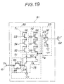
- FIG.19 shows an input buffer circuit 81 which constitutes the second embodiment of the present invention.
- these parts having identical construction to those corresponding parts in FIG.11 will be given identical reference numerals and the description thereof will be omitted.
- the input buffer circuit 81 comprises an inverter 82 and a level shift circuit constructed identically to the level shift circuit 23.
- the inverter 82 comprises the depletion type FETs 53 - 58, another depletion type FET 83, the enhancement type FETs 59 and 60 and a capacitor 84.
- the FETs 53 - 58 and the FETs 59 and 60 are connected similarly to the circuit 51 of FIG.11. Further, a same source voltage is used.
- the circuit 81 has a generally similar construction to the circuit 51 and operates similarly.
- the circuit 81 differs from the circuit 51 in that it has the depletion type FET 83 connected in series between the input terminal 61 and the gate of the FET 59.
- the FET 83 has a drain connected to the input terminal 61 and a source connected to the gate of the FET 59. Further, the FET has a gate connected to its source.
- the capacitor 84 is connected across the source and drain of the FET 83.
- the FET 83 and the capacitor 84 forms a circuit part 91 and the input buffer circuit 81 has a construction such that the circuit part 91 is added to the buffer circuit 51 of FIG.11.
- the FET 83 may be the HEMT device or GaAs MESFET device.
- the current supplied to the gate of the FET 59 is limited by the depletion type FET 83 connected to operate in the saturated region.
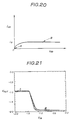
- the FET 83 acts as a constant current source and the current at the gate of the FET 59 does not exceed a level I0 corresponding to an operational point B shown in FIG.20 even when there is a large voltage applied across the source and drain through the input terminal 61.
- the FET 83 connected limits the current to the gate of the FET 59 and the unwanted rise of the low level state is successfully eliminated.
- FIG.21 shows the transfer characteristic of the input buffer circuit 81 having the FET 83 connected in series to the gate of the FET 59. As can be clearly seen from FIG.21, the level of the point B is definitely lower than that of the point B′ in FIG.17.
- FIG.22 shows such a response of the circuit 81 to a series of input signals having a rectangular waveform for a case in which the threshold voltage V TD is changed from - 0.3 volts to - 0.8 volts with an interval of 0.1 volts while fixing the threshold voltage V TE at 0.25 volts. It can be seen from the drawing that there appears a delay in response particularly when the threshold level of the depletion type FETs is changed.
- FIG.23 shows the transient response of the input buffer circuit 81 which is further provided with the capacitor 84.
- the response of the circuit is significantly improved.
- the capacitor 84 may be a diode applied with a reversed bias voltage.
- the operation of the circuit 81 will be described with reference to FIG.19.
- the ECL signal applied to the input terminal 61 has a level lower than the threshold level of the enhancement type FET 59
- the FET 59 is turned off and the voltage appearing at a node V M shown in FIG.19 is substantially zero.
- This voltage is shifted by the level shift circuit 23 and supplied to the output terminal 62 as an output signal of the input buffer circuit 81.
- the level shift circuit 23 By setting the level shift circuit 23 such that a voltage of about one volt is obtained as the output voltage in this state, compatibility with the DCFL device is achieved.
- the FET 59 When the input voltage is increased, the FET 59 is turned on and the voltage V s appears at the drain of the FET 59. In this state, the voltage appearing across the gate and source of the enhancement type FET 60 is represented as V in - V s and thus the FET 60 does not turn on yet. Thus, the voltage at the node V M is substantially zero and the output voltage of about one volt is obtained from the level shift circuit 23. The operation so far corresponds to a point A shown in FIG.20.
- both the FET 59 and the FET 60 are turned on and the node V M assumes a voltage level which is higher than the low level used in the DCFL device by an amount equal to the voltage across the FETs 59 and 60.
- This voltage at the node V M is then shifted by the level shift circuit 23 and is converted to the low level of the DCFL device. This operation is represented by the point B in FIG.21.
- the voltage applied to the FET 83 becomes zero and the transfer characteristic becomes identical to the case in which the FET 83 is not provided.
- voltage is applied across the gate and source of the FET 59 and current flows through the FET 59.
- the FET 83 is provided, the current flowing in to the gate of the FET 59 is limited as already described and the voltage is divided by the FET 83 and FET 59.
- the input buffer circuit of the present embodiment provides a transfer characteristic which is stabilized against variation of the FETs constituting the circuit and an improved and stable transient characteristic. Further, the low level state in the transfer characteristic is lowered and the operational margin of the circuit is extended. Furthermore, the load of circuits supplying the input signal to the buffer circuit is also reduced.
Description
- The present invention generally relates to buffer circuits, and more particularly to an input buffer circuit for converting a logic level of an input signal having an ECL (emitter-coupled-logic) level to a signal having a logic level suitable for use in a compound semiconductor integrated circuit.
- There are various semiconductor devices such as bipolar ECL devices, n-MOS (metal-oxide-semiconductor) devices, GaAs MESFET (gallium arsenide metal-semiconductor field effect transistor) devices, HEMT (high electron mobility transistor) devices and the like that are used in high speed logic integrated circuits. Among others, silicon-based bipolar ECL devices are used most commonly.
- Generally, the logic level (voltage level) used in the silicon-based ECL device called ECL level is different from the logic level used in the compound semiconductor devices such as GaAs MESFET or HEMT. Therefore, there is a need to achieve a compatibility between the logic levels when devices of different type are used in a same system.
- For example, when a part of high speed arithmetic unit using ECL devices is to be replaced by MESFET or HEMT devices, an input/output buffer circuit is needed for achieving compatibility between the ECL device and other devices. Such an input/output buffer circuit is required to have a characteristic which is stable against the variation of the characteristic of the semiconductor devices used therein.
- There are a number of designs for high speed logic gates of GaAs integrated circuits that are developed so as to meet various requirements such as low electrical power, short delay time, large scale of integration, appropriate source voltage level, appropriate logic amplitude, high operational frequency, easy manufacturing process, high yield, and the like. From the view point of large scale integration and low power consumption, integrated circuits of FET are preferred and various devices such as HEMT or GaAs MESFET are studied intensively.
- While there are various designs for the logic circuit based on the FET of GaAs or other compound semiconductor integrated circuits, a DCFL (direct coupled FET logic) device comprising an enhancement type FET and a depleiton type FET acting as a load of the enhancement type FET is particularly preferred from the view point of integration density, simple construction, small size, low power consumption, high operational speed and the like. Thus, the DCFL device is expected to play a major role in the logic gates of the future LSI (large scale integrated circuit) or VLSI (very large scale integrated circuit) devices.
- As already noted, there is a need to provide an input buffer circuit to achieve compatibility of the logic level of the signals when the DCFL device or other devices based on compound semiconductor is used in combination with the ECL device.
- Conventionally three types of input buffer circuits are known for achieving compatibility between the ECL device and the DCFL device.
- Referring to FIGS.1 and 2 at first, the first type of the prior art input buffer circuit uses two depletion type FETs and an inverter circuit in combination for producing a signal to be supplied to the following circuit which may be the DCFL device. As shown in FIG.1, the buffer circuit represented by a circuit 1 comprises a
level shift circuit 2 and aninverter 3. Thelevel shift circuit 2 comprises a pair ofdepleiton type FETs FET 5, a gate and a source of the FET 5 are connected each other, and a drain of theFET 4 is connected to the ground. The source of theFET 5 is further connected to a constant voltage source supplying a source voltage of - 3.6 volts. Theinverter 3, on the other hand, comprises adepletion type FET 6 and an enhancement type FET 7 connected in series, wherein a source of theFET 6 is connected to a drain of the FET 7, a drain of theFET 6 is connected to the ground, and a source of the FET 7 is connected to a constant voltage source supplying a source voltage of - 2 volts. Further, the source of the FET 4 is connected to a gate of the FET 7. Thus, thelevel shift circuit 2 shifts the level of an input signal having the ECL level applied to a gate of theFET 4 and a signal having a level adapted to the following circuit is produced after inversion in theinverter 3. In this circuit 1, one can change the amount of shift by choosing a gate width of theFETs FETs 6 and 7 properly so that the current flowing through these FETs is increased. - This prior art buffer circuit 1, however, has the following problems.
- As the
level shift circuit 2 is constructed by twoFETs FETs FETs FET 4 is connected to the source voltage of - 3.6 volts via theFET 5 having the gate and the source connected and acting as a constant current source, a voltage VSG appearing across the source and gate of theFET 4 is changed. Further, when the threshold voltage of theFET 6 is varied, the operational characteristic of theinverter 3 is also changed. Unfortunately, the variation of the threshold voltage is relatively common in the current compound semiconductor FETs. Such a variation is caused also as a result of the side gate effect which will be described later. - FIG.2 shows such a change of the transfer characteristic of the buffer circuit 1. Referring to FIG.2, the abscissa represents an input voltage Vin applied to the gate of the
FET 4 and the ordinate represents an output voltage Vout obtained from the drain of the FET 7 for a case in which the threshold voltage of the enhancement type FET 7, designated as VTE, is fixed at 0.25 volts and the threshold voltage of thedepletion type FETs - In the buffer circuit of FIG.1 using - 3.6 volts for the source voltage of the
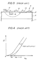
level shift circuit 2, there appears a side gate effect which modifies the threshold voltage of theFET 4 as will be explained. Responsive thereto, the transfer characteristic of the circuit is shifted from the designed or desired characteristic. - Next, the side gate effect will be explained with reference to FIG.3 showing a schematic structure of the
depletion type FET 4. Note that the FET 4 is a HEMT device. Referring to FIG.3, theFET 4 is constructed on a GaAs substrate 11 and comprises a GaAsepitaxial layer 12 having a predetermined layered structure grown epitaxially on the GaAs substrate 11, an AlGaAs (aluminium gallium arsenide)epitaxial layer 12′ further grown epitaxially on thelayer 12, asource electrode 13, agate electrode 14 and adrain electrode 15 each provided on thelayer 12′, anisolation structure 16 formed in thelayer 12, and anelectrode 17 also on thelayer 12′ for application of the voltage of - 3.6 volts. - In such a structure, the electrical field created by the
electrode 17 extends beyond theisolation structure 16 to a region under thegate electrode 14 particularly when the magnitude of the voltage applied to theelectrode 17 is large such as - 3.6 volts, and responsive thereto, the electrical potential in the region under thegate electrode 14 is changed which in turn causes a modification of the threshold level Vth of theFET 4. Such an effect is known as the side gate effect. It is said that such a change of the electrical potential is caused by electrons trapped in the surface state which in turn is developed at a boundary between the GaAs substrate 11 and theepitaxial layer 12′. - The side gate effect can be observed most clearly in a plot of a square root source-drain current versus source-drain voltage shown in FIG.4. In this plot, the current flowing through the
FET 4 with a so-called square root-law extends generally straight with the source-drain voltage VSG and has an intercept at the abscissa indicative of the threshold voltage Vth of the FET. When there appears the side gate effect, the characteristic curve is shifted as shown in the drawing, and together with this, the threshold voltage Vth is changed to Vth + ΔV. As a result, the operational characteristic of the buffer circuit 1 is significantly effected. This side gate effect arises as a result of use of large source voltage (- 3.6 volts) as already noted. When one could increase a distance L between theelectrode 17 and thegate 14, the side gate effect is of course reduced. However, such a measure is contradictory to the requirement to increase the integration density and hence the operational speed of the device. Thus, the side gate effect has been a serious problem in the integrated circuit of compound semiconductor devices such as HEMT. - Accordingly, the applicant of the present invention proposed a buffer circuit shown in FIG.5 in which the use of the source voltage of -3.6 volts is eliminated. Referring to FIG.5, the buffer circuit is represented by a
reference numeral 21 and comprises aninverter 22 for inverting an input signal supplied thereto and a level shift (level conversion)circuit 23 for shifting an output level of theinverter 22. Theinverter 22 comprises depletion type FETs 24 - 26 andenhancement type FETs FET 28 and also a drain connected to a drain of theFET 28. Note thatFETs level shift circuit 23, on the other hand, comprises a series connection of anenhancement type FET 29 and adepletion type FET 30, wherein the FET 30 has a source and a gate connected to each other. Further, the drain of theFET 24 is connected to the ground, a drain of theFET 29 also connected to the ground, a source of theFET 28 connected to a constant voltage source supplying a source voltage of - 2 volt, and the source of theFET 30 connected to the constant voltage source. - When an input voltage having a level higher than the threshold level of of the
FET 27 is applied to a gate of theFET 27, theFET 27 is turned on and a finite voltage is applied to the gate of theFET 28. When the voltage exceeds the threshold voltage of theFET 28, theFET 28 is turned on. Thus, the inversion of theinverter 22 is basically determined by a sum of the threshold voltage of theFETs - Next, elimination of the aforementioned problems pertinent to the circuit of FIG.1 according to this prior art circuit will be described with reference to FIGS.6(A) and (B) as well as FIGS.7(A) and (B).
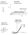
- FIG.6(A) shows a
depletion type FET 31 having a gate and source connected each other. When a FET is connected as such, the FET shows a voltage versus current characteristic shown in FIG.6(B) wherein the ordinate represents a source-drain current ISD and the abscissa represents a source-drain voltage VSD. As can be seen in FIG.6(B), there is an extensive saturated region where the current ISD remains substantially the same with increase of the source-drain voltage VSD. When there is a change in the threshold voltage in theFET 31 connected as shown in FIG.6(A), the current level in the saturated region is changed as shown in FIG.6(B). Thus, there is a substantial change of the current level responsive to the variation of the threshold level. This connection of the FET 31 is similar to the connection of the FET 5 described with reference to FIG.1. - When the FET is connected as shown in the
FET 32 of FIG.7(A), on the other hand, such a change in the current level does not occur even when there is a variation in the threshold voltage of theFET 32. In theFET 32 connected as shown in FIG.7(A), there holds a relation between the drain voltage, gate voltage, source voltage and the threshold voltage as

where VGS stands for a voltage across the gate and drain of theFET 32 and VDS stands for a voltage across the drain and source of the FET. - In the inequality (1), Vth assumes a negative value and VGS and VDS assume an identical voltage level. Thus, the left hand side of the inequality is always larger than the term in the right hand side. This means that the
depletion type FET 32 is operated in the unsaturated region and in such a case there holds a relation


where ISD stands for the source-drain current of theFET 32 and K is a constant. FIG.7(B) shows the characteristic defined by Eq.(2) graphically. It can be seen that the variation of the current ISD caused by the variation of the threshold voltage of theFET 32 is generally very small. - FIG.8 shows a result of simulation undertaken for the
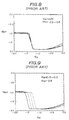
buffer circuit 21. Note that FIG.8 shows the transfer characteristic. In the simulation, it was assumed that a threshold voltage VTE for theFETs buffer circuit 21 is stable against change in the threshold voltage of the depletion FET. Further, the circuit is less sensitive to the side gate effect as the use of the source voltage of - 3.6 volts which has been the cause of the side gate effect in the circuit of FIG.1 is now eliminated by changing the source voltage to - 2 volts. - This
circuit 21, so far successful in eliminating the aforementioned problems, turned out to be unsatisfactory because of the following two problems. -
- As the
FET 27 and theFET 28, both of the enhancement type, are connected to form the Darlington's pair, the effect of the threshold voltage of the enhancement type FET on the threshold characteristic of theinverter 22 and hence thebuffer circuit 21 is doubled. FIG.9 shows the transfer characteristic for the case of thecircuit 21 wherein the threshold voltage VTD of the FETs 24 - 26 and 30 are fixed at - 0.5 volts while the threshold voltage VTE of theFETs buffer circuit 21 changes significantly with the variation of the threshold voltage. - In the
circuit 21, the voltage level appearing at a node A of FIG.5 is indefinite and thecircuit 21 tends to exhibit unstability in the operation. This leads to a poor transient characteristic. - Further, there is another
buffer circuit 33 shown in FIG.10. Referring to FIG.10, thecircuit 33 comprises alevel shift part 34, anotherlevel shift part 35,differential part 36 and areference part 37, in which thelevel shift parts level shift circuit 2 used in the buffer circuit of FIG.1. Thus, thelevel shift part 34 comprises a pair ofdepletion type FETs level shift part 35 comprises a pair ofdepletion type FETs 40 and 41. It should be noted that an input signal to thebuffer circuit 33 is applied to a gate of theFET 38 and a reference voltage produced by thereference part 37 is applied to a gate of theFET 40. Thedifferential part 36 comprises a pair ofdepletion type FETs enhancement type FETs 44 and 45 respectively connected to theFETs depletion type FET 46 having a source and gate connected to each other, wherein the FET 44 and theFET 45 have respective sources connected in common to a drain of theFET 46. The FET 44 receives a signal subjected to level shifting from thelevel shift part 34 and theFET 45 receives a reference yoltage also subjected to level shifting from thereference part 37 via thelevel shift part 35. This reference voltage supplied to theFET 45 is used as the logic threshold in thedifferential part 36. - The
reference part 37 comprises adepletion type FETs FETs level shift parts differential part 36. Thereference part 37 on the other hand receives a source voltage of - 2 volts. Thus, this circuit has a problem in that the variation of the threshold voltage of the FETs causes a significant change in the transfer characteristic similarly to the case of thelevel shift circuit 2 in the buffer circuit of FIG.1. Further, there is another problem in that the reference voltage produced by thereference part 37 is changed responsive to the variation in the threshold voltage of theFETs differential circuit 36. Further, thecircuit 33 suffers from the side gate effect as a result of the use of the source voltage which is set to - 3.6 volts. According to the experiment, thebuffer circuit 33 is more sensitive to the side gate effect than the buffer circuit 1. - EP-A-0 313 810 concerning state of the art according to article 54(3) EPC discloses a source-follower emitter-coupled-logic receiver circuit for interfacing between small emitter-coupled-logic circuit voltage levels and larger field effect transistor circuits voltage level. The circuit comprises an input terminal to which an input signal is applied, a first voltage source, namely the positive supply voltage, a second voltage source, namely ground, first resistance means formed by a first transistor; the source of which is coupled to the positive supply voltage, a first enhancement type FET provided between the drain of the first transistor and ground and the gate of which is connected to the input terminal. Further, a second resistance means formed by a second transistor and a second enhancement type FET is provided, wherein the gate of the second enhancement type FET is connected to the input terminal and the source is connected to the drain of the first enhancement FET. The second transistor is provided between the positive supply voltage and the drain of the second enhancement type FET. The gate of the second transistor is connected to a predetermined voltage. As it will be obvious from the above, this circuit works as a differential amplifier with a current source controlled by the input signal.
- A further prior art document according to article 54(3) is EP-A-0 292 713. Therein, a low voltage swing CMOS receiver or buffer circuit is disclosed. The circuit comprises a first series circuit having first and second P channel transistors (second and first enhancement FETs), and a first N channel transistor (second resistance means) and a second series circuit having second and third N channel transistors (first resistance means) with the third N channel transistor connected as a diode. The first series circuit with an output terminal is connected between a voltage supply terminal and a point of reference potential, such as ground, and the second series circuit is connected from the common point between the first and second P channel and ground. An input terminal is connected to the control electrodes of the first and second P channel transistors and of the first N channel transistor, as well as to the control electrode of the third N channel transistor.
- EP-A-0 154 337 discloses a transistor circuit with hyteresis operation for converting a logical level of an input signal. The circuit includes a level change detector circuit and a threshold selector circuit. The level change detector circuit is formed with a P channel MOS transistor (second resistance means) and an first N channel MOS transistor (second enhancement FET). The source of the P channel transistor is connected to a positive power supply terminal. The gate of this transistor receives an input signal, and the drain thereof provides an output signal which is anti-phasic to the input signal. The drain and the gate of the N channel transistor are connected to the drain and gate of the P channel transistor, respectively. The threshold selector circuit is formed with second and third N channel MOS transistors (first enhancement FET, first resistance means). The drain of second transistor is connected to the source of first N channel transistor, and the gate of second transistor receives the input signal. The source of second transistor is connected to a circuit-ground. The drain of third transistor is connected to the power supply terminal. The gate of third transistor receives the output signal, and the source thereof is connected to the drain of second transistor.
- Accordingly, it is a general object of the present invention to provide a novel and useful input buffer circuit wherein the afore-mentioned problems are eliminated.
- Another and more specific object of the present invention is to provide an input buffer circuit wherein the side gate effect causing variation in the threshold voltage of field effect transistors is successfully eliminated.
- Another object of the present invention is to provide an input buffer circuit wherein the effect of variation in the threshold voltage of field effect transistors on the transfer characteristic of the input buffer circuit is minimized.
- Another object of the present invention is to provide an input buffer circuit having an excellent transient characteristic.
- Another object of the present invention is to provide an input buffer circuit having a stable transient characteristic.
- Another object of the present invention is to provide an input buffer circuit having a large operational margin.
- Another object of the present invention is to provide an input buffer circuit which reduces the load of a driving circuit in a preceding stage for driving the input buffer circuit.
- Another object of the present invention is to provide a buffer circuit comprising an inversion circuit and a level shift circuit, wherein said inversion circuit comprises a first voltage source for supplying a first predetermined voltage, a second voltage source for supplying a second predetermined voltage which is lower than said first predetermined voltage, a first load resistance having a first end connected to the first voltage source, a first enhancement type field effect transistor having a source connected to a second end of the first load resistance and a drain connected to said second voltage source, said first enhancement type field effect transistor having a gate connected to an input terminal of the buffer circuit, a second load resistance having a first end connected to the first voltage source, a second enhancement type field effect transistor having a drain connected to a second end of the second load resistance, said second enhancement type field effect transistor having a source connected to the drain of said first enhancement type field effect transistor and a gate connected to the input terminal of the buffer circuit, and wherein said level shift circuit is connected to the drain of the second enhancement type field effect transistor. According to the present invention, transfer characteristic of the buffer circuit does not change substantially even when there is a variation of the threshold voltage in the field effect transistors as the voltage drop caused across the source and drain of the first enhancement type field effect transistor compensates the variation of the threshold voltage either in the first and second enhancement type field effect transistors. Further, the buffer circuit of the present invention successfully eliminates the side gate effect by using the source voltage having a small magnitude. Further, the buffer circuit has an excellent transient characteristic because of the elimination of Darlington's connection for the first and second enhancement type field effect transistors. Further, by providing a third depletion type field effect transistor having its gate connected to its source such that a drain thereof is connected to an input terminal of the buffer circuit and the source thereof is connected to the gate of the first enhancement type field effect transistor, excessive input current to the first enhancement type field effect transistor is suppressed and the low level state appearing in the transfer characteristic is shifted lower. Accordingly, the load viewed from succeeding circuits is reduced and the operational margin of the buffer circuit is increased. Further, by providing a capacitor across the drain and source of the third depletion type field effect transistor, an excellent transient characteristic can be achieved.
- Other objects and further features of the present invention will become apparent from the following detailed description when read in conjunction with attached drawings.
-
- FIG.1 is a circuit diagram showing a prior art input buffer circuit;
- FIG.2 is a diagram showing a transfer characteristic of the circuit of FIG.1;
- FIG.3 is a diagram for explaining the side gate effect taking place in the circuit of FIG.1;
- FIG.4 is another diagram showing the side gate effect;
- FIG.5 is a circuit diagram showing another prior art input buffer circuit;
- FIGS.6(A) and (B) are diagrams showing a known connection of a depletion type field effect transistor with its source and gate connected and a voltage versus current characteristic of the transistor thus connected;
- FIGS.7(A) and (B) are diagrams showing a known connection of a depletion type field effect transistor with its drain and gate connected and a voltage versus current characteristic of the transistor thus connected;
- FIG.8 is a transfer characteristic of the circuit of FIG.5 in which threshold voltage of the depletion type field effect transistor is varied;
- FIG.9 is a transfer characteristic of the circuit of FIG.5 for a case in which threshold voltage of the enhancement type field effect transistor is varied;
- FIG.10 is a circuit diagram showing another prior art input buffer circuit;
- FIG.11 is a circuit diagram showing a first embodiment of the input buffer circuit of the present invention;
- FIG.12 is a voltage versus current characteristic of the circuit of FIG.11;
- FIG.13 is the voltage versus current characteristic of the circuit of FIG.11 under a different condition;
- FIG.14 is a simplified circuit diagram of the circuit of FIG.11;
- FIG.15 is a voltage versus current characteristic of an enhancement type field effect transistor used in the circuit of FIG.11;
- FlG.16 is a voltage versus current characteristic of another enhancement type field effect transistor used in the circuit of FIG.11;
- FIG.17 is a diagram showing a transfer characteristic of the input buffer circuit of FIG.11 for a case in which threshold voltage of depletion type field effect transistor in the circuit is varied;
- FIG.18 is a diagram showing a transfer characteristic of the input buffer circuit for a case in which threshold voltage of enhancement type field effect transistor is varied;
- FIG.19 is a circuit diagram showing a second embodiment of the input buffer circuit of the present invention;
- FIG.20 is a diagram showing a voltage versus current characteristic of a depletion type field effect transistor used in the circuit of FIG.19;
- FlG.21 is a diagram showing a transfer characteristic of the circuit of FIG.19;
- FIG.22 is a diagram shown a transient characteristic of the circuit of FIG.19; and
- FIG.23 is a diagram showing another transient characteristic of the circuit of FIG.19.
-
- Next, a first embodiment of the present invention will be described. Referring to FIG.11, the input buffer circuit represented as a
circuit 51 comprises aninverter 52 and a level shift circuit identically constructed to thelevel shift circuit 23 already described with reference to FIG.5. Thus, the level shift circuit will be designated ascircuit 23 and the description thereof will not be repeated. - The inverter comprises depletion type field effect transistors 53 - 58 and a pair of enhancement type
field effect transistors FETs FET 53 is connected to the ground while a source of the thetransistor 55 is connected to a drain of theenhancement type FET 59. ThisFET 59 in turn has a source connected to a voltage source supplying a source voltage of - 2 volts. Thus, the FETs 53 - 55 and theFET 59 are connected in series between the ground and the voltage source. TheFET 59 has a gate connected to aninput terminal 61 of thebuffer circuit 51 and receives an input logic signal having the ECL level from theinput terminal 61. - Similarly, the FETs 56 - 58 are connected in series wherein the drain of the
FET 56 is connected to the ground and a source of the FET 58 is connected to a drain of theenhancement type FET 60. TheFET 60 has a source connected to the drain of theFET 59 and a gate connected to theinput terminal 61 commonly with the gate of theFET 59. Theinverter 52 thus constructed supplies an output signal from the drain of theFET 60 to thelevel shift circuit 23 for level shifting, and a signal thus subjected to level shifting is supplied to the following stage (not shown) through anoutput terminal 62. - In the
buffer circuit 51, a part of thecircuit 51 including the FETs 53 - 55 designated by areference numeral 71 and a part of the circuit including the FETs 56 - 58 designated by areference numeral 72 respectively act as load to theFETs inverter 52 including theFETs reference numeral 73 is an essential part of the present invention and has a connection designed such that the variation of the threshold voltage in theFETs inverter 52 as will be described later. When the depletion type FETs used in thecircuits input buffer circuit 51 has another feature in that the side gate effect is minimized by setting the source voltage to - 2 volts. - Next, each of the circuit part will be described in detail.
- As already noted, the FETs 53 - 55 in the
circuit part 71 or the FETs 56 - 58 in thecircuit part 72 has a connection in which the gate and drain are connected each other in each of the transistors. As a result of the connection, the FETs are operated in the linear region and the change of the operational characteristic of each of the FETs is minimized similarly to the FETs 24 - 26 shown in FIG.5. The operational principle of the FETs having such a connection is already described with reference to FIG.5 as well as FIGS.7(A) and (B) and will not be repeated. - FIG.13 shows a voltage versus current characteristic of the FETs 53 - 58 wherein the ordinate represents a source-drain current ISD and the abscissa represents a source-drain voltage VSD. As is already described with reference to FIG.7(A), the transistors 53 - 58 connected as such operate in the linear region and the characteristic curve simulated for the actual FETs is stable against the variation of the threshold voltage. FIG.12 on the other hand shows, for the purpose of comparison, a hypothetical case in which the FETs 53 - 58 are connected as shown in FIG.6(A). As is already noted therein, the FETs thus connected operate in the saturated region and a characteristic similar to FIG.6(B) is obtained. Note that the variation of the source-drain current for this hypothetical case is several times larger than that for the case of FIG.13 which corresponds to the connection of FIG.11. Thus, it is clear that by connecting the FETs 53 - 58 as shown in FIG.11, one can significantly reduce the variation of the source-drain current passing through these FETs even there is a variation in the threshold voltage.
- As already noted, the
circuit part 73 is designed to minimize the change of transfer characteristic responsive to the variation of theenhancement type FETs - First, the operational principle of the
circuit part 73 will be described with reference to FIG.14 which shows theinverter 52 in a simplified form. Thus, thecircuit part 71 and thecircuit part 72 acting as the load to theFETs - FIG.15 shows the voltage versus current characteristic of the
enhancement type FET 59 and FIG.16 shows the voltage versus current characteristic of theenhancement type FET 60 following theFET 59. In the analysis described below, it is assumed that the characteristic curve of theFET 59 is crossed with a load line in the unsaturated region while the characteristic curve of theFET 60 is crossed with the load line in the saturated region. - Designating the voltage appearing at a node connecting the drain of the
FET 59 to the source of theFET 60 as Vs, the currents I₁, I₁+I₂ and I₂ are respectively represented by the following equations:


where Vin stands for an input voltage, Vout stands for an output voltage of theinverter 52, VT stands for the threshold voltage of theFETs - Note that the current I₁+I₂ given by Eq.(4) is determined by the characteristic of the
FET 59 as the currents I₁ and I₂ both flows through theFET 59. There are two possible operational characteristics for theFET 59, one in the saturated region and the other in the unsaturated region. Eq.(4) is for the operation in the unsaturated region. The current I₂ on the other hand flows explicitly through theFET 60 and therefore is determined by the operational characteristic of theFET 60. It is assumed that theFET 60 operates in the saturated region as can be seen from Eq.(6). - Next, a case is considered in which the threshold voltage of the
enhancement type FETs loads FETs


- In Eq.(8), the term (Vin - VT) is rewritten from an original expression which has a form


FET 60 is operated in the unsaturated region. - The foregoing description can be simplified as follows. When the threshold voltage of the
FETs transistor 59 is reduced which results in the increase of the source-drain current flowing through theFET 59. Responsive thereto, the drain voltage of theFET 59 is decreased. This decrease of the drain voltage in turn results in the descrease of the source voltage of theFET 60 and the threshold characteristic of the inverter to turn theFET 60 on becomes substantailly identical to the case where there is no increase in the threshold voltage of theFET 60. In an opposite case where the threshold voltage of theFETs FET 59 is increased which results in the decrease of the drain-source current flowing through theFET 59. Associated therewith, the drain voltage of theFET 59 as well as the source voltage of theFET 60 is increased and the threshold characteristic of the inverter viewed form its input side does not change virtually. - FIGS.17 and 18 show result of simulation undertaken for the
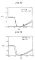
input buffer circuit 51. Referring to FIG.17 showing the transfer characteristic of thebuffer circuit 51 for a case in which the threshold voltage VTD of the FETs 53 - 58 and as well as theFET 30 is changed from - 0.3 volts to - 0.8 volts with an interval of 0.1 volt while fixing the threshold voltage VTE of theFETs - FIG.18, on the other hand, shows the transfer characteristic of the buffer circuit for a case in which the threshold voltage VTE of the
enhancement type FETs FET 30 at - 0.5 volts. From FIG.18, it can be seen that the transfer characteristic shifts to the right by about 0.05 volts responsive to a variation of the threshold voltage VTE amounting 0.05 volts. From the comparison of FIG.9 and FIG.18, it is very clear that theinput buffer circuit 51 has the transfer characteristic which changes substantially less responsive to the same variation of the threshold voltage of theenhancement type FETs buffer circuit 21 having the transfer characteristic of FIG.9, the threshold voltage change of ΔV causes the shift of the characteristic curve which amounts as much as 2ΔV. In the case of thebuffer circuit 51 of FIG.11, on the contrary, a same change of the threshold voltage causes the shift amounting only ΔV. Generally, change of the threshold voltage by ΔV in a circuit comprising a pair of FETs connected in series causes a change of output voltage of 2ΔV. In thebuffer circuit 51 of FIG.11, this commonly accepted relation does not hold and the amount of shift of the transfer characteristic responsive to the change of the threshold voltage in the enhancement type FETs is reduced to a half as is represented in Eqs.(3) - (10) and as is supported by FIG.18. - Further, the
input buffer circuit 51 uses the source voltage set to - 2 volts and the variation of the threshold voltage caused by the side gate effect is suppressed. Further, the change of the transfer characteristic due to the variation of the threshold voltage of the depletion type FETs used in thecircuit parts input buffer circuit 51 is stable against the variation of the threshold voltage of both the enhancement type and depletion type FETs. Furthermore, there is an advantage in that the logic threshold level can be set to the desired level relatively easily as the logic level is set by the enhancement type FET. - The
input buffer circuit 51 described heretofore is preferred from the reasons set forth before. Thiscircuit 51, however, is turned out to have a problem in that the low level in the transfer characteristic is raised when a high level ECL signal having a level of - 0.8 volts is applied to theinput terminal 61. When such a high level ECL signal is applied, a voltage of 1.2 volt appears across the gate and source of theFET 59 and a large current flows through the Schottky gate of theFET 59. In the description hereinafter, a second embodiment of the input buffer circuit of the present invention for eliminating this problem will be described. - FIG.19 shows an
input buffer circuit 81 which constitutes the second embodiment of the present invention. In FIG.19, these parts having identical construction to those corresponding parts in FIG.11 will be given identical reference numerals and the description thereof will be omitted. - Referring to FIG.19, the
input buffer circuit 81 comprises aninverter 82 and a level shift circuit constructed identically to thelevel shift circuit 23. Thus, the level shift circuit will be designated as thecircuit 23 and the description thereof will not be repeated. Theinverter 82 comprises the depletion type FETs 53 - 58, anotherdepletion type FET 83, theenhancement type FETs capacitor 84. The FETs 53 - 58 and theFETs circuit 51 of FIG.11. Further, a same source voltage is used. Thus, thecircuit 81 has a generally similar construction to thecircuit 51 and operates similarly. - The
circuit 81, however, differs from thecircuit 51 in that it has thedepletion type FET 83 connected in series between theinput terminal 61 and the gate of theFET 59. Thus, theFET 83 has a drain connected to theinput terminal 61 and a source connected to the gate of theFET 59. Further, the FET has a gate connected to its source. Furthermore, thecapacitor 84 is connected across the source and drain of theFET 83. TheFET 83 and thecapacitor 84 forms acircuit part 91 and theinput buffer circuit 81 has a construction such that thecircuit part 91 is added to thebuffer circuit 51 of FIG.11. Similarly to other FETs used in the buffer circuit, theFET 83 may be the HEMT device or GaAs MESFET device. - Before describing the operation of the
circuit 81 including thecircuit part 91, a description will be given on the problem of thecircuit 51 which lacks thecircuit part 91 to illuminate the feature of the circuit of the present embodiment. - When a high level ECL signal having the level of - 0.8 volts is applied to the
input terminal 61 of thebuffer circuit 51, there appears a voltage of 1.2 volts across the gate and source of theFET 59. Thereby, the forward voltage or clamp voltage of the Schottky gate is exceeded and a large current flows into theFET 59 through its gate. When such a large current is flowed through theFET 59 having a resistance designated as Rs, the voltage level at the drain of theFET 59 is raised and there appears a tendency that the low level state in the transfer characteristic rises as illustrated by a point B′ in FIG. 17. Further, such a large current increases the load of external driving circuits (not shown) driving the input buffer circuit. Thus, it is necessary to limit the current flowing into theFET 59 from theinput terminal 61. When the low level state in the region at the right hand side of the point B′ of FIG.17 is suppressed, the difference between the high level and the low level is increased and the operational margin of the buffer circuit is increased. - In the present embodiment, the current supplied to the gate of the
FET 59 is limited by thedepletion type FET 83 connected to operate in the saturated region. As shown in the voltage versus current characteristic in FIG.20, theFET 83 acts as a constant current source and the current at the gate of theFET 59 does not exceed a level I₀ corresponding to an operational point B shown in FIG.20 even when there is a large voltage applied across the source and drain through theinput terminal 61. Thus, theFET 83 connected limits the current to the gate of theFET 59 and the unwanted rise of the low level state is successfully eliminated. - FIG.21 shows the transfer characteristic of the
input buffer circuit 81 having theFET 83 connected in series to the gate of theFET 59. As can be clearly seen from FIG.21, the level of the point B is definitely lower than that of the point B′ in FIG.17. - This buffer circuit, though provided with the
FET 83, still has a problem in that there appears a delay in the response of the buffer circuit as the current supplied to the gate of these FETs is limited by theFET 83 and the time needed to charge up the capacitance at the gate of theFETs circuit 81 to a series of input signals having a rectangular waveform for a case in which the threshold voltage VTD is changed from - 0.3 volts to - 0.8 volts with an interval of 0.1 volts while fixing the threshold voltage VTE at 0.25 volts. It can be seen from the drawing that there appears a delay in response particularly when the threshold level of the depletion type FETs is changed. - In order to improve such a transient characteristic of the
buffer circuit 81, thecapacitance 84 is provided in parallel to theFET 83 so that the high frequency current flows freely through thecapacitor 84 and the charge up of theFETs input buffer circuit 81 which is further provided with thecapacitor 84. As can be seen from the drawing, the response of the circuit is significantly improved. Although there remains some delay in the response of FIG.23, such a delay can be completely eliminated by optimizing thecapacitor 84. Of course, any device that provide capacitance can be used for thecapacitor 84. For example, thecapacitor 84 may be a diode applied with a reversed bias voltage. - Hereinafter, the operation of the
circuit 81 will be described with reference to FIG.19. When the ECL signal applied to theinput terminal 61 has a level lower than the threshold level of theenhancement type FET 59, theFET 59 is turned off and the voltage appearing at a node VM shown in FIG.19 is substantially zero. This voltage is shifted by thelevel shift circuit 23 and supplied to theoutput terminal 62 as an output signal of theinput buffer circuit 81. By setting thelevel shift circuit 23 such that a voltage of about one volt is obtained as the output voltage in this state, compatibility with the DCFL device is achieved. - When the input voltage is increased, the
FET 59 is turned on and the voltage Vs appears at the drain of theFET 59. In this state, the voltage appearing across the gate and source of theenhancement type FET 60 is represented as Vin - Vs and thus theFET 60 does not turn on yet. Thus, the voltage at the node VM is substantially zero and the output voltage of about one volt is obtained from thelevel shift circuit 23. The operation so far corresponds to a point A shown in FIG.20. - With a still higher voltage applied to the
input terminal 61, both theFET 59 and theFET 60 are turned on and the node VM assumes a voltage level which is higher than the low level used in the DCFL device by an amount equal to the voltage across theFETs level shift circuit 23 and is converted to the low level of the DCFL device. This operation is represented by the point B in FIG.21. - In the operational point A, the voltage applied to the
FET 83 becomes zero and the transfer characteristic becomes identical to the case in which theFET 83 is not provided. When in the operational point B, however, voltage is applied across the gate and source of theFET 59 and current flows through theFET 59. As theFET 83 is provided, the current flowing in to the gate of theFET 59 is limited as already described and the voltage is divided by theFET 83 andFET 59. - As described heretofore, the input buffer circuit of the present embodiment provides a transfer characteristic which is stabilized against variation of the FETs constituting the circuit and an improved and stable transient characteristic. Further, the low level state in the transfer characteristic is lowered and the operational margin of the circuit is extended. Furthermore, the load of circuits supplying the input signal to the buffer circuit is also reduced.
Claims (6)
- An input buffer circuit for converting a logic level of an input logic signal comprising an inversion circuit (52, 82) supplied with the input logic signal for inverting the logic level thereof, said inversion circuit (52, 82) comprising an input terminal (61) to which said input signal is applied, a first voltage source (ground) for supplying a first predetermined voltage, a second voltage source (-2V) for supplying a second predetermined voltage having a level lower than that of said first predetermined voltage; first resistance means (71) having a first end connected to the first voltage source, a first enhancement type field effect transistor (59) having a drain connected to a second end of the first resistance means, a source connected to said second voltage source and a gate connected to said input terminal, second resistance means (72) having a first end connected to the first voltage source, and a second enhancement type field effect transistor (60) having a drain connected to a second end of the second resistance means, a source connected to the drain of said first enhancement type field effect transistor and a gate connected to the gate of the first enhancement type field effect transistor, said first and second resistance means (71, 72) comprising a serial connection of depletion type field effect transistors (53 - 54, 56 - 58) wherein each of the depletion type field effect transistors has a drain connected to a gate of the same field effect transistor.
- An input buffer circuit as claimed in claim 1 characterized in that each of said first and second resistance means (71, 72) comprises three Schottky gate field effect transistors (53 - 55, 56 - 58).
- An input buffer circuit as claimed in claim 1 characterized in that the level of said second predetermined voltage is lower than the level of said first predetermined voltage by about 2 volts.
- An input buffer circuit as claimed in claim 1 further characterized by current limiting means (91) provided between the input terminal (61) and the gate of the first enhancement type field effect transistor (59) for limiting a current passing therethrough at a predetermined current level.
- An input buffer circuit as claimed in claim 4 characterized in that said current limiting means (91) comprises a depletion type field effect transistor (83) having a drain connected to the input terminal (61), a source connected to the gate of the first enhancement type field effect transistor and a gate connected to the source of the same depletion type field effect transistor, and a capacitor (84) connected across the drain and source of the depletion type field effect transistor.
- An input buffer circuit as claimed in claim 1 characterized in that said input buffer circuit further comprises a level shift circuit (23) connected to receive an output signal of the inverter for shifting a level thereof, said level shift circuit comprises a third enhancement type field effect transistor (29) and a depletion type field effect transistor (30) connected in series, wherein said third enhancement type field effect transistor has a drain connected to the first voltage source, a gate connected to the drain of the second enhancement type field effect transistor (60) and a source connected to a drain of the depletion type field effect transistor, and said depletion type field effect transistor has a source and a gate connected in common to the second voltage source.
Applications Claiming Priority (2)
| Application Number | Priority Date | Filing Date | Title |
|---|---|---|---|
| JP63216732A JPH0263319A (en) | 1988-08-30 | 1988-08-30 | Input buffer |
| JP216732/88 | 1988-08-30 |
Publications (3)
| Publication Number | Publication Date |
|---|---|
| EP0356986A2 EP0356986A2 (en) | 1990-03-07 |
| EP0356986A3 EP0356986A3 (en) | 1990-09-19 |
| EP0356986B1 true EP0356986B1 (en) | 1994-04-13 |
Family
ID=16693062
Family Applications (1)
| Application Number | Title | Priority Date | Filing Date |
|---|---|---|---|
| EP89115900A Expired - Lifetime EP0356986B1 (en) | 1988-08-30 | 1989-08-29 | Buffer circuit for logic level conversion |
Country Status (5)
| Country | Link |
|---|---|
| US (1) | US5051626A (en) |
| EP (1) | EP0356986B1 (en) |
| JP (1) | JPH0263319A (en) |
| KR (1) | KR920005359B1 (en) |
| DE (1) | DE68914548D1 (en) |
Families Citing this family (10)
| Publication number | Priority date | Publication date | Assignee | Title |
|---|---|---|---|---|
| DE69119643T2 (en) * | 1990-03-15 | 1996-09-26 | Fujitsu Ltd | Buffer circuit for logical level conversion |
| JPH0595267A (en) * | 1991-10-02 | 1993-04-16 | Sumitomo Electric Ind Ltd | Semiconductor logic device |
| JP3365804B2 (en) * | 1993-01-12 | 2003-01-14 | 株式会社日立製作所 | Communication line drive circuit, interface LSI, and communication terminal device |
| US5420527A (en) * | 1994-04-06 | 1995-05-30 | Itt Corporation | Temperature and supply insensitive TTL or CMOS to 0/-5 V translator |
| JPH08204536A (en) * | 1995-01-20 | 1996-08-09 | Fujitsu Ltd | Interface circuit and level conversion circuit |
| US6147540A (en) * | 1998-08-31 | 2000-11-14 | Motorola Inc. | High voltage input buffer made by a low voltage process and having a self-adjusting trigger point |
| KR20030007299A (en) * | 2002-12-04 | 2003-01-23 | (주) 바이탈인터내셔날 | A bag having integrated light-emitting device |
| US8154320B1 (en) * | 2009-03-24 | 2012-04-10 | Lockheed Martin Corporation | Voltage level shifter |
| CN111786642A (en) * | 2020-07-10 | 2020-10-16 | 无锡英迪芯微电子科技股份有限公司 | Push-pull structure port output circuit with port voltage protection function |
| CN114070297A (en) * | 2020-08-05 | 2022-02-18 | 圣邦微电子(北京)股份有限公司 | Level flip circuit with micro power consumption and method for reducing transient current in circuit |
Citations (3)
| Publication number | Priority date | Publication date | Assignee | Title |
|---|---|---|---|---|
| EP0154337A2 (en) * | 1984-03-06 | 1985-09-11 | Kabushiki Kaisha Toshiba | Transistor circuit for semiconductor device with hysteresis operation and manufacturing method therefor |
| EP0292713A2 (en) * | 1987-05-26 | 1988-11-30 | International Business Machines Corporation | Low voltage swing CMOS receiver circuit |
| EP0313810A2 (en) * | 1987-10-30 | 1989-05-03 | International Business Machines Corporation | Source-follower emitter-coupled-logic receiver circuit |
Family Cites Families (3)
| Publication number | Priority date | Publication date | Assignee | Title |
|---|---|---|---|---|
| JPS5550743A (en) * | 1978-10-11 | 1980-04-12 | Fujitsu Ltd | Level shift circuit |
| US4791322A (en) * | 1987-05-19 | 1988-12-13 | Gazelle Microcircuits, Inc. | TTL compatible input buffer |
| US4767951A (en) * | 1987-06-30 | 1988-08-30 | Hewlett-Packard Company | ECL to NMOS converter |
-
1988
- 1988-08-30 JP JP63216732A patent/JPH0263319A/en active Pending
-
1989
- 1989-08-29 KR KR1019890012350A patent/KR920005359B1/en not_active IP Right Cessation
- 1989-08-29 DE DE68914548T patent/DE68914548D1/en not_active Expired - Lifetime
- 1989-08-29 EP EP89115900A patent/EP0356986B1/en not_active Expired - Lifetime
-
1990
- 1990-11-09 US US07/610,461 patent/US5051626A/en not_active Expired - Fee Related
Patent Citations (3)
| Publication number | Priority date | Publication date | Assignee | Title |
|---|---|---|---|---|
| EP0154337A2 (en) * | 1984-03-06 | 1985-09-11 | Kabushiki Kaisha Toshiba | Transistor circuit for semiconductor device with hysteresis operation and manufacturing method therefor |
| EP0292713A2 (en) * | 1987-05-26 | 1988-11-30 | International Business Machines Corporation | Low voltage swing CMOS receiver circuit |
| EP0313810A2 (en) * | 1987-10-30 | 1989-05-03 | International Business Machines Corporation | Source-follower emitter-coupled-logic receiver circuit |
Also Published As
| Publication number | Publication date |
|---|---|
| JPH0263319A (en) | 1990-03-02 |
| DE68914548D1 (en) | 1994-05-19 |
| EP0356986A3 (en) | 1990-09-19 |
| US5051626A (en) | 1991-09-24 |
| KR920005359B1 (en) | 1992-07-02 |
| EP0356986A2 (en) | 1990-03-07 |
| KR900004111A (en) | 1990-03-27 |
Similar Documents
| Publication | Publication Date | Title |
|---|---|---|
| KR940006619B1 (en) | Buffer circuit | |
| EP0110701B1 (en) | Input buffer circuit | |
| US5021691A (en) | Level conversion circuit having capability of supplying output signal with controlled logical level | |
| US5136182A (en) | Controlled voltage or current source, and logic gate with same | |
| EP0075915B1 (en) | Logic circuit operable by a single power voltage | |
| JPH03500114A (en) | New family of anti-noise logic gates and memory cells | |
| IE960781A1 (en) | Circuits with dynamically biased active loads | |
| US5543746A (en) | Programmable CMOS current source having positive temperature coefficient | |
| EP0356986B1 (en) | Buffer circuit for logic level conversion | |
| US4701643A (en) | FET gate current limiter circuits | |
| KR900009192B1 (en) | Differential circuit | |
| US4724342A (en) | Push-pull DCFL driver circuit | |
| US4016434A (en) | Load gate compensator circuit | |
| EP0226678B1 (en) | Logic circuit | |
| US5646551A (en) | Mixed mode output buffer circuit for CMOSIC | |
| US4883985A (en) | Mesfet latch circuit | |
| US4713559A (en) | Multiple input and multiple output or/and circuit | |
| KR920004906B1 (en) | Fet logic circuit | |
| KR900000068B1 (en) | Semiconductor device | |
| US6023157A (en) | Constant-current circuit for logic circuit in integrated semiconductor | |
| EP0314476A2 (en) | Feedback threshold compensation | |
| EP0356108A2 (en) | Source follower field-effect logic gate (SFFL) suitable for III-V technologies | |
| US6727743B2 (en) | Semiconductor integrated circuit for holding an output signal of an output terminal in a non-operating state | |
| US5087836A (en) | Electronic circuit including a parallel combination of an E-FET and a D-FET | |
| US5696453A (en) | GaAs logic circuit with temperature compensation circuitry |
Legal Events
| Date | Code | Title | Description |
|---|---|---|---|
| PUAI | Public reference made under article 153(3) epc to a published international application that has entered the european phase |
Free format text: ORIGINAL CODE: 0009012 |
|
| AK | Designated contracting states |
Kind code of ref document: A2 Designated state(s): DE FR GB |
|
| PUAL | Search report despatched |
Free format text: ORIGINAL CODE: 0009013 |
|
| AK | Designated contracting states |
Kind code of ref document: A3 Designated state(s): DE FR GB |
|
| 17P | Request for examination filed |
Effective date: 19901115 |
|
| 17Q | First examination report despatched |
Effective date: 19920728 |
|
| GRAA | (expected) grant |
Free format text: ORIGINAL CODE: 0009210 |
|
| AK | Designated contracting states |
Kind code of ref document: B1 Designated state(s): DE FR GB |
|
| PG25 | Lapsed in a contracting state [announced via postgrant information from national office to epo] |
Ref country code: DE Effective date: 19940413 |
|
| REF | Corresponds to: |
Ref document number: 68914548 Country of ref document: DE Date of ref document: 19940519 |
|
| ET | Fr: translation filed | ||
| PG25 | Lapsed in a contracting state [announced via postgrant information from national office to epo] |
Ref country code: GB Effective date: 19940829 |
|
| PLBE | No opposition filed within time limit |
Free format text: ORIGINAL CODE: 0009261 |
|
| STAA | Information on the status of an ep patent application or granted ep patent |
Free format text: STATUS: NO OPPOSITION FILED WITHIN TIME LIMIT |
|
| 26N | No opposition filed | ||
| GBPC | Gb: european patent ceased through non-payment of renewal fee |
Effective date: 19940829 |
|
| PGFP | Annual fee paid to national office [announced via postgrant information from national office to epo] |
Ref country code: FR Payment date: 19950809 Year of fee payment: 7 |
|
| PG25 | Lapsed in a contracting state [announced via postgrant information from national office to epo] |
Ref country code: FR Effective date: 19970430 |
|
| REG | Reference to a national code |
Ref country code: FR Ref legal event code: ST |