EP0348632B1 - Behandlung von Grundplatten für Leiterplatten - Google Patents
Behandlung von Grundplatten für Leiterplatten Download PDFInfo
- Publication number
- EP0348632B1 EP0348632B1 EP89107717A EP89107717A EP0348632B1 EP 0348632 B1 EP0348632 B1 EP 0348632B1 EP 89107717 A EP89107717 A EP 89107717A EP 89107717 A EP89107717 A EP 89107717A EP 0348632 B1 EP0348632 B1 EP 0348632B1
- Authority
- EP
- European Patent Office
- Prior art keywords
- cores
- planes
- core
- prepreg
- conductive planes
- Prior art date
- Legal status (The legal status is an assumption and is not a legal conclusion. Google has not performed a legal analysis and makes no representation as to the accuracy of the status listed.)
- Expired - Lifetime
Links
- 238000000034 method Methods 0.000 claims description 25
- 230000002093 peripheral effect Effects 0.000 claims description 10
- 239000003989 dielectric material Substances 0.000 claims description 8
- 239000000853 adhesive Substances 0.000 claims description 7
- 230000001070 adhesive effect Effects 0.000 claims description 7
- 238000007789 sealing Methods 0.000 claims description 4
- 239000011152 fibreglass Substances 0.000 claims description 3
- 238000003475 lamination Methods 0.000 claims description 3
- 238000003801 milling Methods 0.000 claims description 3
- RYGMFSIKBFXOCR-UHFFFAOYSA-N Copper Chemical compound [Cu] RYGMFSIKBFXOCR-UHFFFAOYSA-N 0.000 description 11
- 239000004593 Epoxy Substances 0.000 description 11
- 239000000463 material Substances 0.000 description 11
- 239000000203 mixture Substances 0.000 description 11
- 239000004744 fabric Substances 0.000 description 9
- 239000011521 glass Substances 0.000 description 8
- IISBACLAFKSPIT-UHFFFAOYSA-N bisphenol A Chemical compound C=1C=C(O)C=CC=1C(C)(C)C1=CC=C(O)C=C1 IISBACLAFKSPIT-UHFFFAOYSA-N 0.000 description 6
- 239000011889 copper foil Substances 0.000 description 6
- ISWSIDIOOBJBQZ-UHFFFAOYSA-N phenol group Chemical group C1(=CC=CC=C1)O ISWSIDIOOBJBQZ-UHFFFAOYSA-N 0.000 description 6
- 229920005989 resin Polymers 0.000 description 6
- 239000011347 resin Substances 0.000 description 6
- 229910052802 copper Inorganic materials 0.000 description 5
- 239000010949 copper Substances 0.000 description 5
- 239000002184 metal Substances 0.000 description 5
- 229910052751 metal Inorganic materials 0.000 description 5
- 239000012260 resinous material Substances 0.000 description 5
- 239000003795 chemical substances by application Substances 0.000 description 4
- 238000010030 laminating Methods 0.000 description 4
- BRLQWZUYTZBJKN-UHFFFAOYSA-N Epichlorohydrin Chemical compound ClCC1CO1 BRLQWZUYTZBJKN-UHFFFAOYSA-N 0.000 description 3
- WSFSSNUMVMOOMR-UHFFFAOYSA-N Formaldehyde Chemical compound O=C WSFSSNUMVMOOMR-UHFFFAOYSA-N 0.000 description 3
- 230000009977 dual effect Effects 0.000 description 3
- 239000003822 epoxy resin Substances 0.000 description 3
- LNEPOXFFQSENCJ-UHFFFAOYSA-N haloperidol Chemical compound C1CC(O)(C=2C=CC(Cl)=CC=2)CCN1CCCC(=O)C1=CC=C(F)C=C1 LNEPOXFFQSENCJ-UHFFFAOYSA-N 0.000 description 3
- 229920000647 polyepoxide Polymers 0.000 description 3
- 239000000758 substrate Substances 0.000 description 3
- 239000004952 Polyamide Substances 0.000 description 2
- 239000002131 composite material Substances 0.000 description 2
- 239000012467 final product Substances 0.000 description 2
- 229920003986 novolac Polymers 0.000 description 2
- 229920002120 photoresistant polymer Polymers 0.000 description 2
- 229920002647 polyamide Polymers 0.000 description 2
- 229920000642 polymer Polymers 0.000 description 2
- GHMLBKRAJCXXBS-UHFFFAOYSA-N resorcinol Chemical compound OC1=CC=CC(O)=C1 GHMLBKRAJCXXBS-UHFFFAOYSA-N 0.000 description 2
- 239000000565 sealant Substances 0.000 description 2
- 229920001169 thermoplastic Polymers 0.000 description 2
- 229920001187 thermosetting polymer Polymers 0.000 description 2
- 239000004416 thermosoftening plastic Substances 0.000 description 2
- XLYOFNOQVPJJNP-UHFFFAOYSA-N water Substances O XLYOFNOQVPJJNP-UHFFFAOYSA-N 0.000 description 2
- QTWJRLJHJPIABL-UHFFFAOYSA-N 2-methylphenol;3-methylphenol;4-methylphenol Chemical compound CC1=CC=C(O)C=C1.CC1=CC=CC(O)=C1.CC1=CC=CC=C1O QTWJRLJHJPIABL-UHFFFAOYSA-N 0.000 description 1
- 229920000459 Nitrile rubber Polymers 0.000 description 1
- 239000004743 Polypropylene Substances 0.000 description 1
- 239000002253 acid Substances 0.000 description 1
- 150000007513 acids Chemical class 0.000 description 1
- 229920000122 acrylonitrile butadiene styrene Polymers 0.000 description 1
- 125000002723 alicyclic group Chemical group 0.000 description 1
- 150000008064 anhydrides Chemical class 0.000 description 1
- LMMDJMWIHPEQSJ-UHFFFAOYSA-N bis[(3-methyl-7-oxabicyclo[4.1.0]heptan-4-yl)methyl] hexanedioate Chemical compound C1C2OC2CC(C)C1COC(=O)CCCCC(=O)OCC1CC2OC2CC1C LMMDJMWIHPEQSJ-UHFFFAOYSA-N 0.000 description 1
- 239000011248 coating agent Substances 0.000 description 1
- 238000000576 coating method Methods 0.000 description 1
- 239000004020 conductor Substances 0.000 description 1
- 229920001577 copolymer Polymers 0.000 description 1
- 229930003836 cresol Natural products 0.000 description 1
- 238000006735 epoxidation reaction Methods 0.000 description 1
- 125000003700 epoxy group Chemical group 0.000 description 1
- 239000011888 foil Substances 0.000 description 1
- 125000002485 formyl group Chemical class [H]C(*)=O 0.000 description 1
- 239000011968 lewis acid catalyst Substances 0.000 description 1
- 238000004519 manufacturing process Methods 0.000 description 1
- 229920001568 phenolic resin Polymers 0.000 description 1
- IGALFTFNPPBUDN-UHFFFAOYSA-N phenyl-[2,3,4,5-tetrakis(oxiran-2-ylmethyl)phenyl]methanediamine Chemical compound C=1C(CC2OC2)=C(CC2OC2)C(CC2OC2)=C(CC2OC2)C=1C(N)(N)C1=CC=CC=C1 IGALFTFNPPBUDN-UHFFFAOYSA-N 0.000 description 1
- 239000004033 plastic Substances 0.000 description 1
- 229920003023 plastic Polymers 0.000 description 1
- 229920002492 poly(sulfone) Polymers 0.000 description 1
- 229920000768 polyamine Polymers 0.000 description 1
- 229920000515 polycarbonate Polymers 0.000 description 1
- 239000004417 polycarbonate Substances 0.000 description 1
- 229920000098 polyolefin Polymers 0.000 description 1
- -1 polypropylene Polymers 0.000 description 1
- 229920001155 polypropylene Polymers 0.000 description 1
- 239000005077 polysulfide Substances 0.000 description 1
- 229920001021 polysulfide Polymers 0.000 description 1
- 150000008117 polysulfides Polymers 0.000 description 1
- 229920002620 polyvinyl fluoride Polymers 0.000 description 1
- 238000003825 pressing Methods 0.000 description 1
- 150000003141 primary amines Chemical class 0.000 description 1
- 239000012744 reinforcing agent Substances 0.000 description 1
- 230000003014 reinforcing effect Effects 0.000 description 1
- 239000003566 sealing material Substances 0.000 description 1
- 150000003335 secondary amines Chemical class 0.000 description 1
- 238000000926 separation method Methods 0.000 description 1
- 239000007787 solid Substances 0.000 description 1
- 150000003512 tertiary amines Chemical class 0.000 description 1
Images
Classifications
-
- H—ELECTRICITY
- H05—ELECTRIC TECHNIQUES NOT OTHERWISE PROVIDED FOR
- H05K—PRINTED CIRCUITS; CASINGS OR CONSTRUCTIONAL DETAILS OF ELECTRIC APPARATUS; MANUFACTURE OF ASSEMBLAGES OF ELECTRICAL COMPONENTS
- H05K3/00—Apparatus or processes for manufacturing printed circuits
- H05K3/02—Apparatus or processes for manufacturing printed circuits in which the conductive material is applied to the surface of the insulating support and is thereafter removed from such areas of the surface which are not intended for current conducting or shielding
- H05K3/06—Apparatus or processes for manufacturing printed circuits in which the conductive material is applied to the surface of the insulating support and is thereafter removed from such areas of the surface which are not intended for current conducting or shielding the conductive material being removed chemically or electrolytically, e.g. by photo-etch process
-
- H—ELECTRICITY
- H05—ELECTRIC TECHNIQUES NOT OTHERWISE PROVIDED FOR
- H05K—PRINTED CIRCUITS; CASINGS OR CONSTRUCTIONAL DETAILS OF ELECTRIC APPARATUS; MANUFACTURE OF ASSEMBLAGES OF ELECTRICAL COMPONENTS
- H05K3/00—Apparatus or processes for manufacturing printed circuits
- H05K3/0097—Processing two or more printed circuits simultaneously, e.g. made from a common substrate, or temporarily stacked circuit boards
-
- H—ELECTRICITY
- H05—ELECTRIC TECHNIQUES NOT OTHERWISE PROVIDED FOR
- H05K—PRINTED CIRCUITS; CASINGS OR CONSTRUCTIONAL DETAILS OF ELECTRIC APPARATUS; MANUFACTURE OF ASSEMBLAGES OF ELECTRICAL COMPONENTS
- H05K2203/00—Indexing scheme relating to apparatus or processes for manufacturing printed circuits covered by H05K3/00
- H05K2203/11—Treatments characterised by their effect, e.g. heating, cooling, roughening
- H05K2203/1147—Sealing or impregnating, e.g. of pores
-
- H—ELECTRICITY
- H05—ELECTRIC TECHNIQUES NOT OTHERWISE PROVIDED FOR
- H05K—PRINTED CIRCUITS; CASINGS OR CONSTRUCTIONAL DETAILS OF ELECTRIC APPARATUS; MANUFACTURE OF ASSEMBLAGES OF ELECTRICAL COMPONENTS
- H05K2203/00—Indexing scheme relating to apparatus or processes for manufacturing printed circuits covered by H05K3/00
- H05K2203/15—Position of the PCB during processing
- H05K2203/1536—Temporarily stacked PCBs
-
- H—ELECTRICITY
- H05—ELECTRIC TECHNIQUES NOT OTHERWISE PROVIDED FOR
- H05K—PRINTED CIRCUITS; CASINGS OR CONSTRUCTIONAL DETAILS OF ELECTRIC APPARATUS; MANUFACTURE OF ASSEMBLAGES OF ELECTRICAL COMPONENTS
- H05K3/00—Apparatus or processes for manufacturing printed circuits
- H05K3/46—Manufacturing multilayer circuits
- H05K3/4611—Manufacturing multilayer circuits by laminating two or more circuit boards
-
- Y—GENERAL TAGGING OF NEW TECHNOLOGICAL DEVELOPMENTS; GENERAL TAGGING OF CROSS-SECTIONAL TECHNOLOGIES SPANNING OVER SEVERAL SECTIONS OF THE IPC; TECHNICAL SUBJECTS COVERED BY FORMER USPC CROSS-REFERENCE ART COLLECTIONS [XRACs] AND DIGESTS
- Y10—TECHNICAL SUBJECTS COVERED BY FORMER USPC
- Y10T—TECHNICAL SUBJECTS COVERED BY FORMER US CLASSIFICATION
- Y10T29/00—Metal working
- Y10T29/49—Method of mechanical manufacture
- Y10T29/49002—Electrical device making
- Y10T29/49117—Conductor or circuit manufacturing
- Y10T29/49124—On flat or curved insulated base, e.g., printed circuit, etc.
- Y10T29/49155—Manufacturing circuit on or in base
- Y10T29/49158—Manufacturing circuit on or in base with molding of insulated base
-
- Y—GENERAL TAGGING OF NEW TECHNOLOGICAL DEVELOPMENTS; GENERAL TAGGING OF CROSS-SECTIONAL TECHNOLOGIES SPANNING OVER SEVERAL SECTIONS OF THE IPC; TECHNICAL SUBJECTS COVERED BY FORMER USPC CROSS-REFERENCE ART COLLECTIONS [XRACs] AND DIGESTS
- Y10—TECHNICAL SUBJECTS COVERED BY FORMER USPC
- Y10T—TECHNICAL SUBJECTS COVERED BY FORMER US CLASSIFICATION
- Y10T29/00—Metal working
- Y10T29/49—Method of mechanical manufacture
- Y10T29/4981—Utilizing transitory attached element or associated separate material
- Y10T29/49812—Temporary protective coating, impregnation, or cast layer
Definitions
- the present invention is concerned with a method for processing cores for circuit boards or cards.
- the present invention is concerned with simultaneously processing two cores which involves temporarily bonding them together around the peripheral face planes for processing and then separating them when simultaneous processing is completed.
- the method of the present invention is especially advantageous for producing relatively thin cores for circuit boards or cards.
- the method of the present invention permits the handling of relatively thin cores on the high volume equipment that is commercially employed.
- the thickness of the core for circuit boards and cards for various high volume processing has been in the order of about 300 ⁇ m or greater.
- the cores contain a signal pattern on one side and a blank uncircuitized metallic layer on the other side which can later be made into the external composite surface.
- the metal such as the copper on the side which is to function as the blank uncircuitized layer during the photoprocessing
- a photosensitive material which will remain as such during the photoprocessing, and then be removed in its entirety.
- the method of the present invention overcomes the above-discussed problems with respect to the prior art.
- the method of the present invention allows for the handling of relatively thin cores on the high volume equipment used in prior processes that have required cores of much greater thickness, such as about 300 ⁇ m or more.
- the method of the present invention as claimed includes providing two cores, each being a dielectric material having conductive planes on both major surfaces thereof.
- the two cores are temporarily bonded or fixed together by sealing the peripheral face planes thereof with a seal providing two internal adjacent conductive planes and two external conductive planes.
- the two external conductive planes are simultaneously processed to thereby form signal patterns thereon.
- the seal from the peripheral face planes is then removed and the cores are separated from each other, thereby simultaneously providing the two cores, each having one signal conductive plane and one uncircuitized conductive plane.
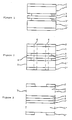
- Figures 1-3 are schematic illustrations exemplifying the method of the present invention.
- the present invention is concerned with producing cores for circuit boards or cards whereby two cores are simultaneously processed.
- the method of the present invention includes providing two cores, each being a dielectric material having conductive planes on both major surfaces thereof.
- the dielectric materials employed include thermoplastic and thermosetting resins.
- thermosetting resinous materials include epoxy, phenolic-based materials, and polyamides. Such materials are usually molded of the resinous material, along with a reinforcing agent such as being a glass-filled epoxy or phenolic-based material.
- phenolic-type materials examples include copolymers of phenol, resorcinol, and cresol.
- thermoplastic polymeric materials examples include polyolefins such as polypropylene, polysulfones, polycarbonates, nitrile rubbers, and ABS polymers.
- the preferred polymeric materials employed in accordance with the present invention are epoxy resinous materials.
- Typical epoxy resins include the bisphenol A type resins obtained from bisphenol A and epichlorohydrin; brominated bisphenol A type resins from tetrabrominated bisphenol A and epichlorohydrin; resinous materials obtained by the epoxidation of novolak resins produced from a phenolic material such as phenol and an aldehyde such as formaldehyde with epichlorohydrin; epoxidized non-linear novolaks having at least about six terminal epoxy groups such as EPI-REZ SU8; polyfunctional epoxy resins such as tetraglycidyldiaminodiphenyl methane and alicyclic epoxy resins such as bis(3,4-epoxy-6-methylcyclohexyl methyl) adipate.
- the epoxy resinous compositions also can contain accelerating agents and curing agents as well-known in the art.
- suitable curing agents include polyamines, primary, secondary, and tertiary amines, polyamides, polysulfides, dicyanamide, urea-phenol-formaldehyde, and acids or anhydrides thereof.
- suitable curing agents include Lewis acid catalysts such as BF 3 and complexes thereof.
- the preferred epoxy compositions are those disclosed in U.S. Patent 3,523,037 to Chellis.
- prepreg substrates which contain a resin and a reinforcing fabric such as fiberglass.
- Such compositions containing fabric are usually prepared by impregnating the fabric with, for example, an epoxy polymer composition.
- the amount of epoxy composition is usually about 30% to about 70% by weight and preferably about 50% to about 65% by weight of the total solids content of the epoxy composition in the fiberglass.
- a particular glass fabric employed has a single ply thickness of about 40 ⁇ m and is a woven glass, a typical one being 106 style woven glass fabric.
- Other typical glass fabrics range, for instance, from style 104 (30 ⁇ m single ply thickness) to style 141 (280 ⁇ m single ply thickness).
- the composition is cured to the B-stage and cut to the desired shape, such as a sheet.
- the single ply thickness is usually about 35,5 ⁇ m for 104 style glass to about 200 ⁇ m. However, thicker sheets can be employed if desired.
- the single ply thickness is about 46 ⁇ m thick.
- a typical multi-ply thickness of a core is about 130 ⁇ m.
- the curing to the B-stage is usually achieved by using temperatures of about 80°C to about 110°C for about 3-10 minutes.
- the now-impregnated fabric or prepreg can be divided into sheets of desired size, typical of which is about 60 x 70 cm which is somewhat larger than the desired final product which is about 50 x 60 cm.
- the number of individual sheets of prepreg to provide any given core can vary greatly, such as from 1 to about 20 or more, depending upon the desired final product, among other factors.
- about 2 or 3 sheets of the prepreg are interleaved between sheets of electrolytic copper foil placed between two polished metal plates. This assembly of prepregs and metal plates and copper foil is then placed between platens of a laminating press. The platens are cored for steam or super-heated water so that they can be heated to elevated temperatures.
- the above assembly is subjected to pressures which may vary from about 0.35 N/mm 2 to about 14 N/mm 2 , depending upon the resin content, flow of the prepreg and laminate temperatures.
- the pressures are about 2.0 N/mm 2 to about 3.5 N/mm 2 .
- the laminate temperature is preferably about 150°C to about 200°C, typically about 175°C.
- the time of the pressing operation is variable depending upon the particular materials employed and the pressure applied. About 1 hour is adequate for the above conditions.
- the laminate is cooled down to room temperature in about 1 hour by introducing cool water into the platens of the laminating press.
- a typical copper foil employed on the surface that is to provide the signal patterns is about 30 g per m 2 and is about 36 ⁇ m thick.
- a typical copper foil employed on the surface for the subsequent uncircuitized plane is 15 g per m 2 and is about 18 ⁇ m thick.
- other foils can be used on either surfaces if desired, such as 28.35 g (1 ounce) on the surfaces to provide the subsequent uncircuitized planes.
- one of the copper foils will be sized so that it is smaller than the copper foil on the opposite side of the dielectric substrate.
- the two cores have one of their major surfaces abutting the major surface of the other core such that the internal adjacent conductive planes are shorter than the external conductive planes (see Figure 1).
- the copper on the inside need only be about 0.6 cm from the edges of the dielectric. However, it must be larger than the final dimensions of the core which, for a typical core, will be about 52 cm x 63 cm. In a typical arrangement, the copper on the internal planes is about 58 cm x 69 cm for a dielectric of about 60 cm x 70 cm.
- a dual-sided adhesive sheet could be placed between the internal planes at lamination. These sheets could then be readily removed at the time of separation of the two cores, such as by employing a simple, properly sized pneumatic tool having double piano-like wires to separate the adhesive sheet from the internal metal such as copper planes.
- a preferred material for this purpose is a laminated prepreg of the same type as used for the prepreg of the core.
- a typical laminate has about four (4) plies of the prepreg. It is prelaminated to the dimensions of the cores during processing (e.g. - 60 x 70 cm). Such is prepared by laminating about 4 plies of prepreg interleaved between sheets of a smooth plastic such as Tedlar (a trade designation of Du Pont) placed between two polished metal plates.
- the two cores are then temporarily fixed together by sealing the peripheral face planes thereof.
- the face planes can be sealed by employing, for example, an epoxy composition such as the same epoxy composition as used to form the prepregs is the preferred procedure.
- the two individual cores can be individually prelaminated or, in the case of the presence of the intermediate sheet, the two cores can be produced by simultaneous lamination in the same laminating press with the intermediate sheet located between the plies for the individual cores.
- the intermediate sheet separates the plies for one core from the plies for the other core.
- the two external conductive planes are then simultaneously processed to thereby form signal patterns on both of the cores.
- the core-set can then be profiled to the final core dimensions such as employing a conventional milling machine.
- the milling operation will, in turn, also remove the sealing material at the peripheral face planes of the cores, thereby making it possible to separate the cores from each other and thereby obtain two separate cores, each having one signal plane and one uncircuitized plane.
- the internal planes were protected during the processing from the developing compositions and thereby did not require coating with any photoresist as required by prior art processes.
- the dual core set is illustrated by two dielectric materials (1,1′) having an external conductive plane (2,2′, respectively) and an internal conductive plane (3,3′, respectively) which preferably is shorter than the external conductive plane.
- an adhesive sheet (4) Intermediate between the two conductive materials and internal adjacent conductive planes is an adhesive sheet (4).
- Figure 2 illustrates the temporarily bonding together by sealing the peripheral face planes with a sealant such as an epoxy composition (5).
- tooling holes (6) can be provided to position the arrangement for the subsequent processing. However, these are not necessary.
- Figure 3 illustrates the profiling of the final core dimension as illustrated by dotted line (7) which, likewise, removes the sealant (5) from the peripheral face planes so that the two cores can be separated from each other. Likewise, the tooling holes are removed during the profiling procedure.
Landscapes
- Engineering & Computer Science (AREA)
- Manufacturing & Machinery (AREA)
- Microelectronics & Electronic Packaging (AREA)
- Production Of Multi-Layered Print Wiring Board (AREA)
- Magnetic Heads (AREA)
Claims (10)
- Verfahren zur Bearbeitung von Grundplatten für Leiterplatten oder -karten, folgendes umfassend:a) Bereitstellen von zwei Grundplatten, von denen jede aus einem dielektrischen Material (1, 1′) mit Leiterebenen (2, 3; 2′, 3′) auf beiden Hauptflächen derselben besteht;b) vorübergehendes Befestigen beider Grundplatten durch Abdichten der peripheren Flächenebenen mit einer Dichtung (5), wodurch zwei interne aneinandergrenzende Leiterebenen (3, 3′) und zwei externe Leiterebenen (2, 2′) entstehen;c) gleichzeitiges Bearbeiten der beiden externen Leiterebenen (2, 2′) zur Bildung von Signalmustern undd) Entfernen der Dichtung (5) von den peripheren Flächenebenen und Trennen der Grundplatten voneinander, wodurch gleichzeitig zwei Grundplatten entstehen, die jeweils eine Signalleiterebene (2, 2′) und eine Schaltkreisleiterebene (3, 3′) aufweisen.
- Verfahren nach Anspruch 1, bei dem die internen aneinandergrenzenden Leiterebenen (3, 3′) kleiner als die externen Leiterebenen (2, 2′), aber größer als die gewünschten Abmessungen der endgültigen Grundplatte sind.
- Verfahren nach Anspruch 1, bei dem das Entfernen der Dichtung (5) von den peripheren Flächenebenen durch Profilieren der Grundplatten auf die gewünschten endgültigen Grundplattenabmessungen erfolgt.
- Verfahren nach Anspruch 3, bei dem das Profilieren durch Fräsen erfolgt.
- Verfahren nach einem der Ansprüche 1 bis 4, bei dem eine Klebfolie (4) zwischen die internen Leiterebenen (3, 3′) gelegt wird.
- Verfahren nach Anspruch 5, bei dem die Klebfolie ein dielektrisches Prepreg (Prepreg = vorimprägniertes Glasgewebe) ist.
- Verfahren nach einem der Ansprüche 1 bis 6, bei dem das dielektrische Material (1, 1′) 2 bis 3 Prepregfolien umfaßt, von denen jede ca. 46 µm dick ist.
- Verfahren nach Anspruch 7, bei dem das Prepreg ein Expoxidfaserglasprepreg ist.
- Verfahren nach einem der Ansprüche 1 bis 8, bei dem jede Grundplatte ein Mehrfachlaminat und einzeln vorlaminiert ist.
- Verfahren nach Anspruch 5, bei dem jede Grundplatte ein Mehrfachlaminat ist, und die beiden Grundplatten durch gleichzeitiges Laminieren mit der die Schichten einer Grundplatte von den Schichten der anderen trennenden Klebfolie erzeugt werden.
Applications Claiming Priority (2)
| Application Number | Priority Date | Filing Date | Title |
|---|---|---|---|
| US213944 | 1988-06-29 | ||
| US07/213,944 US4918812A (en) | 1988-06-29 | 1988-06-29 | Processing of cores for circuit boards or cards |
Publications (3)
| Publication Number | Publication Date |
|---|---|
| EP0348632A2 EP0348632A2 (de) | 1990-01-03 |
| EP0348632A3 EP0348632A3 (de) | 1991-03-27 |
| EP0348632B1 true EP0348632B1 (de) | 1992-10-14 |
Family
ID=22797139
Family Applications (1)
| Application Number | Title | Priority Date | Filing Date |
|---|---|---|---|
| EP89107717A Expired - Lifetime EP0348632B1 (de) | 1988-06-29 | 1989-04-28 | Behandlung von Grundplatten für Leiterplatten |
Country Status (4)
| Country | Link |
|---|---|
| US (1) | US4918812A (de) |
| EP (1) | EP0348632B1 (de) |
| JP (1) | JPH0233998A (de) |
| DE (1) | DE68903196D1 (de) |
Families Citing this family (10)
| Publication number | Priority date | Publication date | Assignee | Title |
|---|---|---|---|---|
| JPH04154188A (ja) * | 1990-10-18 | 1992-05-27 | Cmk Corp | 片面プリント配線板の製造法 |
| US5505321A (en) * | 1994-12-05 | 1996-04-09 | Teledyne Industries, Inc. | Fabrication multilayer combined rigid/flex printed circuit board |
| EP0732039B1 (de) * | 1993-12-02 | 2001-10-17 | Teledyne Industries, Inc. | Herstellung einer kombinierten starren/flexiblen mehrschichtigen leiterplatte |
| US5877940A (en) * | 1993-12-02 | 1999-03-02 | Teledyne Industries Inc. | Fabrication multilayer combined rigid/flex printed circuit board |
| US5723205A (en) * | 1994-03-08 | 1998-03-03 | Teledyne Industries, Inc. | Fabrication multilayer combined rigid/flex printer circuit board |
| US6145372A (en) * | 1997-04-30 | 2000-11-14 | Texas Instruments Incorporated | Apparatus and method for detecting impurities in wet chemicals |
| EP1063873A3 (de) * | 1999-06-22 | 2003-04-23 | Dr.-Ing. Jürgen Schulz-Harder | Verfahren zum Herstellen von Substraten mit strukturierten Metallisierungen sowie Halte-und Fixierelement zur Verwendung bei dem Verfahren |
| CH691277A5 (de) * | 2000-02-29 | 2001-06-15 | Ascom Ag | Verfahren zur Herstellung von Leiterplatten sowie Leiterplatte. |
| DE10154316A1 (de) * | 2001-11-07 | 2003-05-15 | Juergen Schulz-Harder | Verfahren zur selektiven Oberflächenbehandlung von plattenförmigen Werkstücken |
| JP2006049660A (ja) * | 2004-08-06 | 2006-02-16 | Cmk Corp | プリント配線板の製造方法 |
Family Cites Families (13)
| Publication number | Priority date | Publication date | Assignee | Title |
|---|---|---|---|---|
| NL93768C (de) * | 1957-06-07 | 1960-03-15 | Philips Nv | |
| US3207127A (en) * | 1962-05-31 | 1965-09-21 | Xerox Corp | Apparatus for forming coatings on printed circuit boards |
| FR1566544A (de) * | 1968-03-14 | 1969-05-09 | ||
| JPS5434142B2 (de) * | 1973-09-29 | 1979-10-25 | ||
| JPS555873B2 (de) * | 1974-02-28 | 1980-02-12 | ||
| JPS5259854A (en) * | 1975-11-13 | 1977-05-17 | Matsushita Electric Works Ltd | Method of producing multiilayer printed circuit board |
| US4191800A (en) * | 1976-05-27 | 1980-03-04 | Bell Telephone Laboratories, Incorporated | Devices employing flexible substrates and method for making same |
| JPS5434142A (en) * | 1977-08-23 | 1979-03-13 | Riken Keikinzoku Kogyo Kk | Exhaust duct |
| US4201616A (en) * | 1978-06-23 | 1980-05-06 | International Business Machines Corporation | Dimensionally stable laminated printed circuit cores or boards and method of fabricating same |
| US4606787A (en) * | 1982-03-04 | 1986-08-19 | Etd Technology, Inc. | Method and apparatus for manufacturing multi layer printed circuit boards |
| US4649497A (en) * | 1983-06-03 | 1987-03-10 | John Fluke Mfg. Co., Inc. | Computer-produced circuit board |
| JPS61224497A (ja) * | 1985-03-29 | 1986-10-06 | 東芝ケミカル株式会社 | 多層板の製造方法 |
| JPS6256141A (ja) * | 1985-09-05 | 1987-03-11 | 松下電工株式会社 | 多層プリント配線板 |
-
1988
- 1988-06-29 US US07/213,944 patent/US4918812A/en not_active Expired - Fee Related
-
1989
- 1989-04-28 EP EP89107717A patent/EP0348632B1/de not_active Expired - Lifetime
- 1989-04-28 DE DE8989107717T patent/DE68903196D1/de not_active Expired - Lifetime
- 1989-05-29 JP JP1132920A patent/JPH0233998A/ja active Pending
Also Published As
| Publication number | Publication date |
|---|---|
| DE68903196D1 (de) | 1992-11-19 |
| JPH0233998A (ja) | 1990-02-05 |
| EP0348632A3 (de) | 1991-03-27 |
| US4918812A (en) | 1990-04-24 |
| EP0348632A2 (de) | 1990-01-03 |
Similar Documents
| Publication | Publication Date | Title |
|---|---|---|
| US4659425A (en) | Continuous process for the manufacture of printed circuit boards | |
| US4180608A (en) | Process for making multi-layer printed circuit boards, and the article resulting therefrom | |
| EP0348632B1 (de) | Behandlung von Grundplatten für Leiterplatten | |
| CN111465221B (zh) | 基于射频滤波器的封装基板的制作方法 | |
| JPH02129994A (ja) | 導電性回路部材及びその製造方法 | |
| EP0309684A1 (de) | Verfahren zur Verbesserung des Haftvermögens von Polymeren auf elektrolytischen Kupferoberflächen | |
| JPS62239593A (ja) | 汚染物質の除去方法 | |
| EP0655183B1 (de) | Herstellungsverfahren einer vielschicht-leiterplatte | |
| JPS62214939A (ja) | 積層板の製法 | |
| CN115519850B (zh) | 覆铜板制造方法 | |
| JPH02223436A (ja) | 誘電体による充填方法 | |
| WO1991018491A1 (en) | Process for the production of a multilayer printed circuit board | |
| JPH05138807A (ja) | 銅張積層板の製造法 | |
| US6609294B1 (en) | Method of bulk fabricating printed wiring board laminates | |
| JP3402392B2 (ja) | 多層印刷配線板 | |
| JP4759896B2 (ja) | プリント配線板製造用材料の製造方法 | |
| JPH036093A (ja) | 多層プリント配線板用プリプレグシート | |
| JPH05121872A (ja) | 曲面回路板の製造方法 | |
| JPS63233810A (ja) | 積層板の製造方法 | |
| JPH0748460A (ja) | 積層板 | |
| JP3241504B2 (ja) | リジッドフレックスプリント配線板及びその製造方法 | |
| JPH03285391A (ja) | 多層配線基板の製造方法 | |
| JPH06177539A (ja) | 多層プリント配線板製造方法 | |
| JPH06334278A (ja) | リジッドフレックスプリント配線板 | |
| JPS6046098A (ja) | 多層板の製造方法 |
Legal Events
| Date | Code | Title | Description |
|---|---|---|---|
| PUAI | Public reference made under article 153(3) epc to a published international application that has entered the european phase |
Free format text: ORIGINAL CODE: 0009012 |
|
| AK | Designated contracting states |
Kind code of ref document: A2 Designated state(s): DE FR GB |
|
| 17P | Request for examination filed |
Effective date: 19900419 |
|
| PUAL | Search report despatched |
Free format text: ORIGINAL CODE: 0009013 |
|
| AK | Designated contracting states |
Kind code of ref document: A3 Designated state(s): DE FR GB |
|
| 17Q | First examination report despatched |
Effective date: 19911118 |
|
| GRAA | (expected) grant |
Free format text: ORIGINAL CODE: 0009210 |
|
| AK | Designated contracting states |
Kind code of ref document: B1 Designated state(s): DE FR GB |
|
| PG25 | Lapsed in a contracting state [announced via postgrant information from national office to epo] |
Ref country code: FR Effective date: 19921014 Ref country code: DE Effective date: 19921014 |
|
| REF | Corresponds to: |
Ref document number: 68903196 Country of ref document: DE Date of ref document: 19921119 |
|
| EN | Fr: translation not filed | ||
| PG25 | Lapsed in a contracting state [announced via postgrant information from national office to epo] |
Ref country code: GB Effective date: 19930428 |
|
| PLBE | No opposition filed within time limit |
Free format text: ORIGINAL CODE: 0009261 |
|
| STAA | Information on the status of an ep patent application or granted ep patent |
Free format text: STATUS: NO OPPOSITION FILED WITHIN TIME LIMIT |
|
| 26N | No opposition filed | ||
| GBPC | Gb: european patent ceased through non-payment of renewal fee |
Effective date: 19930428 |