EP0347894B1 - Verfahren zum Betreiben eines IC-Kartenlesers/-schreibers - Google Patents
Verfahren zum Betreiben eines IC-Kartenlesers/-schreibers Download PDFInfo
- Publication number
- EP0347894B1 EP0347894B1 EP89111333A EP89111333A EP0347894B1 EP 0347894 B1 EP0347894 B1 EP 0347894B1 EP 89111333 A EP89111333 A EP 89111333A EP 89111333 A EP89111333 A EP 89111333A EP 0347894 B1 EP0347894 B1 EP 0347894B1
- Authority
- EP
- European Patent Office
- Prior art keywords
- card
- frequency
- data
- signal
- clock pulses
- Prior art date
- Legal status (The legal status is an assumption and is not a legal conclusion. Google has not performed a legal analysis and makes no representation as to the accuracy of the status listed.)
- Expired - Lifetime
Links
Images


Classifications
-
- G—PHYSICS
- G06—COMPUTING OR CALCULATING; COUNTING
- G06K—GRAPHICAL DATA READING; PRESENTATION OF DATA; RECORD CARRIERS; HANDLING RECORD CARRIERS
- G06K7/00—Methods or arrangements for sensing record carriers, e.g. for reading patterns
- G06K7/0008—General problems related to the reading of electronic memory record carriers, independent of its reading method, e.g. power transfer
Definitions
- the present invention relates to a method for operating an IC (Integrated Circuit) card reader/writer apparatus and, more particularly, to a method for operating an IC card reader/writer apparatus for use with a business transactions processing apparatus which is operable with an IC card for executing various kinds of business transactions.
- IC Integrated Circuit
- a card transactions processing apparatus capable of processing various kinds of business transactions data by using an IC card is attracting much attention and has been put to practical use.
- a card transactions processing apparatus may be implemented by a keyboard, a display, a printer, an IC card reader/writer, and a pin pad.
- the processing apparatus having the above construction When the processing apparatus having the above construction is loaded with an IC card, the IC card reader/writer reads data which are stored in the IC card. As one manipulates the keyboard to enter a transaction command and a key, a particular operation procedure or guidance is indicated on the display. When the operator sequentially enters data on the keyboard according to the guidance appearing on the display, the data are transmitted to central equipment to be processed thereby. The result of processing returned from the central equipment may be printed out by the printer of the processing apparatus, as needed.
- an IC card has a particular operating clock frequency which is selected before it is issued.
- the predominant frequency mode selected for IC cards is, for example, 4.9152 megahertz mode in Japan and 3. 579545 megahertz mode in U. S. A and France.
- a prior art IC card reader/writer therefore, has a clock generator implemented by an oscillator exclusively producing clock pulses having a frequency of 4. 9152 megahertz or an oscillator exclusively producing clock pulses whose frequency is 3.579545 megahertz.
- the single-frequency clock generator scheme stated above is undesirable from the standpoint of applicable range. Specifically, when an IC card reader/writer whose clock generator oscillates at a certain fixed clock frequency is loaded with an IC card which is operable in a different frequency mode, the reader/writer cannot read data out of the IC card at all so that the processing apparatus is practically useless.
- EP-A-0 237 883 there is described an IC card system comprising an IC card terminal and an IC card which is inserted into the terminal, the terminal including a power-supply circuit for supplying data-writing power to a memory provided in the IC card, and a timer circuit for measuring a period of time corresponding to the maximum time during which one unit of data can be written into the memory.
- the supply of power to the IC card is renewed every time the IC card sends a request for a unit of data, within the period of time set in the time-measuring circuit.
- the supply of power is stopped when the IC card makes no request for a unit of data within the above-mentioned period of time.
- a method of operating an IC card reader/writer apparatus according to the preamble of claim 1 is also disclosed in EP-A-0 237 883.
- the reader/writer therefore, is capable of operating with two different kinds of IC cards each having a different frequency mode.
- the IC card transactions processing apparatus is usable with IC cards the operating clock frequencies of which are different from each other.
- an IC card transactions processing apparatus is shown and generally designated by the reference numeral 1.
- the processing apparatus 1 is generally made up of a keyboard 2, a display 3, a printer 4, an IC card reader/writer 5, and a pin pad 6.
- the keyboard 2 is located on the top of a front portion of the apparatus 1 and has a plurality of keys arranged thereon.
- the display 3 serves to indicate an operation procedure or guidance and data entered thereon.
- the printer 4 is constituted by a thermal printer or similar printer for printing out data on a slip, for example.
- the IC card reader/writer 5 is capable of reading data out of an IC card and writing data in an IC card, as needed.
- the pin pad 6 may be manipulated by the operator to enter a code number and other specific data which are assigned to an individual.
- the processing apparatus 1 having the above construction will be operated as follows. After a power switch (not shown) of the processor 1 has been turned on, an IC card (not shown) is inserted in the IC card reader/writer 5. Then, the reader/writer 5 reads various kinds of transaction command data and other data particular to the customer out of the IC card while feeding such data to a storage (not shown) which is built in the processing apparatus 1. In this condition, the operator manipulates the keybord 2 to enter a desired transaction command and a key of the IC card being loaded. Then, an operation procedure associated with the particular transaction is indicated on the display 3.
- a transmission control section also built in the processing apparatus 1 sends the entered data to a central station or equipment (not shown).
- the central station executes predetermined processing with the received data and, on completing the processing, reports the end of processing to the terminal or processor 1. This causes the printer 4 of the processor 1 to print out the data on a slip, for example.
- the reader/writer 5 has a one-chip CPU (Central Processing Unit) which supervises the operations of the entire reader/writer 5.
- the CPU 20 has a clock input CLK to which a first clock generator 21 is interconnected.
- the clock generator 21 produces clock pulses whose frequency is 14. 7456 megahertz for clocking the CPU 20. These clock pulses are used to cause an IC card 23 to operate also, as described in detail later.
- An MPU (Micro Processing Unit) 22 is interconnected to the CPU 20 by a bus 20a so that, under the control of the CPU 20, it may interchange data with the IC card 23.
- a power supply circuit 24 is brought into connection with power supply terminals Vcc, 0V and Vpp of the IC card 23.
- Zero volt is applied to the power supply terminal 0V to serve as a reference input voltage, while predetermined different voltages for individually implementing a reading and a writing operation are applied to the power supply terminals Vcc and Vpp.
- a frequency setting circuit 25 is interconnected to the MPU 22 by a bus 22a.
- FIG. 3 shows a specific construction of the frequency setting circuit 25.
- the frequency setting circuit 25 is made up of a frequency divider 26 and a selector 27.
- the frequency divider 26 has a signal input terminal connecting to the bus 22a, a control terminal connecting to the MPU 22 via a signal line 28, and an output terminal connecting to the clock input CLK of the IC card 23 via a signal line 29.
- the selector 27 has a terminal A connecting to the clock output of the CPU 20 via a clock signal line 30, and a terminal B connecting to a second clock generator 32 via a clock signal line 31.
- the second clock generator 32 is implemented by an oscillator which produces reference clock pulses Ps having a frequency of 7. 15909 megahertz.
- the selector 27 has a control terminal C connected to the MPU 22 via a signal line 33, and an output terminal connecting to a clock input terminal of the frequency divider 26 via a signal line 34.
- the IC card 23 stores various kinds of data, or characters, in a particular signal format as prescribed by ISO/IDS 7816-3 ANNEX A.
- the data are made up of initializing data TS, format data TO, operating clock frequency data TA1, operating voltage data TB1, data TC1 representative of a delay between data blocks, a protocol mode TD1 for block transmission, a one-block transmission unit TA2, another operating voltage data TB2 (having priority over the voltage data TB1), and data TC2 representative of a waiting time between data.
- the clock frequency data TA1 to the waiting time data TC2 shown in the figure are representative of interface characters.
- the IC card 23 stores other various kinds of data such as data associated with a customer and transaction command data.
- the IC card 23 is inserted in the IC card reader/writer 5 after the power switch of the processing apparatus 1 has been turned on. Then, the MPU 22 loads a register built therein with a frequency division parameter data 1/ x ( x being 2, for example) while feeding the parameter data to the frequency divider 26 in the form of a parallel signal over the bus 22a. Simultaneously, the MPU 22 delivers a frequency parameter set signal to the frequency divider 26 over the signal line 28. Specifically, the frequency parameter set signal is fed to the control terminal of the frequency divider 26 as a signal having a high level or a low level, whereby the frequency division parameter 1/ x is set in the frequency divider 26.
- the MPU 22 feeds to the control terminal C of the selector 27 a switching signal which has a high level or a low level, over the signal line 33.
- the terminal B of the selector 27 is connected to the clock signal line 34.
- the clock pulses Pc are fed to the clock input CLK of the IC card 23.
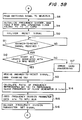
- the frequency divider 26 is initialized by the procedure described so far, as represented by a step S0 in FIG. 5A.
- the step S0 is followed by a step S1 in which the MPU 22 feeds a reset signal Rs to the IC card 23 over the signal line 35 under the control of the CPU 20.
- the IC card 23 returns an answer-to-reset signal to the MPU 22 over the I/O signal line 36 (S2).
- the answer-to-reset signal has a bit length, or start bit length, which is selected in conformity to a standardized transfer rate such as 9800 bits per second.
- the MPU 22 measures the start bit length of the returned answer-to-reset signal to see if the IC card 23 has a frequency mode which it can identify.
- the MPU 22 determines that the IC card 23 has an identifiable frequency mode. Then, on receiving the answer-to-reset signal, the MPU 22 initializes the various units of the IC card processing apparatus 1 on the basis of the initializing data TS while confirming the format of the IC card 23 on the basis of the format data TO (S4). Executing the step S4, the MPU 22 checks the operating clock frequency data TA1 stored in the IC card 23. When the MPU 22 determines that the data TA1 is representative of a frequency of 3.
- step S5 for calculating the ratio of the clock frequency represented by the data TA1 to the frequency of the reference clock pulse Ps (7. 15909 megahertz) being generated by the clock generator 32, i. e. n/m .
- the MPU 22 On determining that the ratio n/m is 1/2, for example, the MPU 22 loads the internal register thereof with frequency parameter data of 1/2 while delivering the frequency parameter data 1/2 to the bus 22a in the form of a parallel signal (S6). At the same time, the MPU 22 executes a step S7 for feeding out a frequency parameter set signal to the signal line 28. As a result the frequency division parameter 1/2 is set in the frequency divider 26.
- the selector 27 has the terminal B connecting to the clock signal line 34, as stated earlier. Hence, the reference clock pulses Ps having a frequency of 7. 15909 megahertz and being generated by the clock generator 32 are fed to the frequency divider 26 over the clock signal line 34.
- the frequency divider 26 divides the input reference clock pulses Ps by the frequency division parameter 1/2, thereby producing clock pulses Pc whose frequency is 3. 579545 megahertz.
- the 3. 579545 megahertz clock pulses are applied to the clock input CLK of the IC card 23, whereby the IC card 23 the operating clock frequency of which is also 3. 579545 megahertz is rendered operative.
- the MPU 22 advances to a step S8 to deliver a high-level or low-level switching signal to the control terminal C of the selector 27 over the signal line 33.
- the selector 27 selects an input appearing on its input terminal A.
- the terminal A is connected by the signal line 30 to the clock output of the CPU 20 on which the clock pulses from the clock generator 21 appear. Consequently, the reference clock pulses Ps having a frequency of 14. 7456 megahertz are routed through the selector 27 and clock signal line 34 to the frequency divider 26.
- the step S8 is followed by a step S9 in which the MPU 22 loads the internal register with a frequency parameter data of 1/ y ( y being 3, for example) while feeding this frequency parameter data 1/ y to thc bus 22a in the form of a parallel signal.
- thc MPU 22 delivers a frequency division parameter set signal to the signal line 28.
- the frequency division parameter data 1/ y is set in the frequency divider 26.
- the frequency divider 26 divides the 14. 7456 megahertz reference clock pulses Ps by the frequency division parameter 1/3, so that clock pulses Ps the frequency of which is 4. 9152 megahertz are fed to the clock input CLK of the IC card 23.
- the frequency divider 26 is initialized by such a sequence of steps.
- the MPU 22 delivers a reset signal Rs to the IC card 23 over the signal line 35 under the control of the CPU 20 (S10).
- the IC card 23 in turn returns an answer-to-reset signal to the MPU 22 over the I/O signal line 36 (S11).
- the MPU 22 measures the start bit length of the answer-to-reset signal to see if the IC card 23 has an identifiable frequency mode (S12). When the start bit length conforms to the transfer rate of 9600 bits per second, the MPU 22 determines that the IC card 23 has a 4. 9152 megahertz mode.
- the MPU 22 On receiving the answer-to-reset signal from the IC card 23, the MPU 22 initializes the various units of the reader/writer 5 on the basis of the initializing data TS while confirming the format of the IC card 23 on the basis of the format data TO (S13).
- the MPU 22 determines that the IC card 23 does not have the 4. 9152 megahertz mode in the step S12, it executes a step S17 assigned to error card processing by deciding that it cannot handle the IC card 23.
- the MPU 22 advances to a step S13 for confirming the operating clock frequency data TA1 of the IC card 23. If the data TA1 is representative of a frequency of 4. 9152 megahertz, the MPU 22 executes a step S14 to calculate the ratio of the clock frequency represented by the data TA1 to the frequency of the reference clock pulses Ps (14. 7456 megahertz) being generated by the clock generator 21, i. e. n/m.
- the MPU 22 On determining that the ratio n/m is 1/3, for example, the MPU 22 loads the internal register thereof with frequency parameter data of 1/3 while delivering the frequency parameter data 1/3 to the bus 22a in the form of a parallel signal (S15). At the same time, the MPU 22 executes a step S16 for feeding out a frequency parameter set signal to the signal line 28 while loading the frequency divider 26 with the frequency division parameter 1/3. Since the reference clock pulses Ps the frequency of which is 14. 7456 megahertz are fed from the clock generator 21 to the frequency divider 26, operating clock pulses Pc having a frequency of 4. 9152 megahertz is applied to the clock input CLK of the IC card 23. Hence, the reader/writer 5 is operable with the IC card 23 which needs clock pulses of 4. 9152 megahertz in the same manner as with the IC card 23 having another frequency mode.
- the reader/writer 5 After the reader/writer 5 has fed operating clock pulses Pc the frequency of which matches the frequency mode of the IC card 23 as stated above, it reads necessary transaction data out of the card 23 to execute ordinary transactions processing.
- the IC card reader/writer has frequency identifying means for identifying an operating clock frequency particular to an IC card by referencing frequency data stored in the card, and a frequency setting circuit for converting, in response to an output of the frequency identifying means, reference clock pulses being generated by a clock generator into clock pulses the frequency of which matches the card.
- the IC card reader/writer therefore, is operable with IC cards having different operating clock frequencies, implementing a wide variety of applications at low cost.
Landscapes
- Engineering & Computer Science (AREA)
- Artificial Intelligence (AREA)
- Computer Vision & Pattern Recognition (AREA)
- Physics & Mathematics (AREA)
- General Physics & Mathematics (AREA)
- Theoretical Computer Science (AREA)
- Credit Cards Or The Like (AREA)
Claims (6)
- Verfahren für den Betrieb einer IC-Karten-Lese-/Schreibvorrichtung (5) mit einer ersten Referenztakterzeugungseinrichtung (32) zum Erzeugen von ersten Referenztaktimpulsen mit einer festgelegten ersten Frequenz zum Zuführen von ersten Taktimpulsen zu einer IC-Karte (23) zum Austauschen von Daten mit der IC-Karte (23), wenn die IC-Karte mit der Vorrichtung verbunden ist, bestehend aus den Schritten:
Zufuhr (S1) eines ersten Rücksetzsignals zusammen mit den ersten Taktimpulsen zu der IC-Karte,
Empfang (S2) des Rücksetz-Antwortsignals (ATR), nachfolgend ATR-Signal genannt, von der IC-Karte (23) als Antwort auf das erste Rücksetzsignal,
Feststellen (S3), ob das ATR-Signal einen identifizierbaren Frequenzwert hat oder nicht,
wenn das ATR-Signal einen identifizierbaren Frequenzwert hat,
Lesen (S4) der Daten des ATR-Signals und
Auswählen (S5-S7) der Betriebsfrequenz, bei welcher die Lese-/Schreibvorrichtung (5) mit der IC-Karte (23) kommuniziert,
gekennzeichnet durch die Schritte:
Vorsehen einer zweiten Referenztakterzeugungseinrichtung (21) zur Erzeugung von zweiten Referenztaktimpulsen mit einer festgelegten zweiten Frequenz zum Zuführen von zweiten Taktimpulsen zu der IC-Karte (23),
wenn das ATR-Signal keinen identifizierbaren Frequenzwert hat,
Initialisierung (S9) der zweiten Referenztakterzeugungseinrichtung (21),
Zufuhr (S10) eines zweiten Rücksetzsignals zusammen mit den zweiten Taktimpulsen zu der IC-Karte (23),
Empfang (S11) des ATR-Signals von der IC-Karte (23) als Antwort auf das zweite Rücksetzsignal,
Feststellen (S12), ob das ATR-Signal einen identifizierbaren Frequenzwert hat oder nicht,
wenn das ATR-Signal einen identifizierbaren Frequenzwert hat,
Lesen (S13) der Daten des ATR-Signals und
Auswählen (S14-S16) der Betriebsfrequenz, bei welcher die Lese-/Schreibvorrichtung (5) mit der IC-Karte (23) kommuniziert,
wenn das ATR-Signal keinen identifizierbaren Frequenzwert hat,
Starten einer Kartenfehlerbearbeitung. - Verfahren nach Anspruch 1, wobei der Schritt des Auswählens der Betriebsfrequenz, bei welcher die Lese-/Schreibvorrichtung (5) mit der IC-Karte (23) kommuniziert, den Schritt der Umwandlung der durch die Referenztakterzeugungseinrichtung (21, 32) erzeugten Referenztaktimpulse in Taktimpulse, die mit der IC-Karte (23) verknüpft sind, beinhaltet.
- Verfahren nach Anspruch 2, das außerdem die Schritte beinhaltet:
Ermittlung der Betriebsfrequenz der Daten des ATR-Signals;
Bereitstellung eines mit dem Ausgang der Referenztakterzeugungseinrichtung (21, 32) verbundenen Frequenzteilers (26);
Auswahl von Frequenzteilungsparameterdaten auf der Basis der festgestellten Betriebsfrequenz für die Frequenzteilung, die durch den Frequenzteiler (26) durchgeführt wird, und
Zufuhr der Frequenzteilungsparameterdaten zu dem Frequenzteiler (26). - Verfahren nach Anspruch 3, das außerdem den Schritt der Bereitstellung eines Wählers (27) zur selektiven Zufuhr von durch die erste Referenztakterzeugungseinrichtung (32) und die zweite Takterzeugungseinrichtung (21) erzeugten Taktimpulsen zu dem Frequenzteiler (26) beinhaltet.
- Verfahren nach einem der Ansprüche 1 bis 4, wobei der Schritt der Ermittlung, ob das ATR-Signal einen identifizierbaren Frequenzwert hat oder nicht, den Schritt des Messens einer Startbitlänge des ATR-Signals von der IC-Karte (23) beinhaltet, um zu sehen, ob die IC-Karte (23) einen identifizierbaren Frequenzwert hat.
- Verfahren nach einem der Ansprüche 1 bis 4, das außerdem die Schritte der Bereitstellung eines Registers und des Ladens dieses Registers mit dem Frequenzteilungsparameter beinhaltet.
Applications Claiming Priority (2)
| Application Number | Priority Date | Filing Date | Title |
|---|---|---|---|
| JP154620/88 | 1988-06-24 | ||
| JP63154620A JPH025192A (ja) | 1988-06-24 | 1988-06-24 | Icカードリーダライタ装置 |
Publications (3)
| Publication Number | Publication Date |
|---|---|
| EP0347894A2 EP0347894A2 (de) | 1989-12-27 |
| EP0347894A3 EP0347894A3 (de) | 1991-07-24 |
| EP0347894B1 true EP0347894B1 (de) | 1995-05-03 |
Family
ID=15588161
Family Applications (1)
| Application Number | Title | Priority Date | Filing Date |
|---|---|---|---|
| EP89111333A Expired - Lifetime EP0347894B1 (de) | 1988-06-24 | 1989-06-22 | Verfahren zum Betreiben eines IC-Kartenlesers/-schreibers |
Country Status (7)
| Country | Link |
|---|---|
| US (1) | US5070233A (de) |
| EP (1) | EP0347894B1 (de) |
| JP (1) | JPH025192A (de) |
| AU (1) | AU607620B2 (de) |
| CA (1) | CA1319195C (de) |
| DE (1) | DE68922439T2 (de) |
| NZ (1) | NZ229581A (de) |
Cited By (1)
| Publication number | Priority date | Publication date | Assignee | Title |
|---|---|---|---|---|
| DE102004062964A1 (de) * | 2004-12-28 | 2006-07-06 | Sigos Systemintegration Gmbh | Testgerät zum Einsatz in einem Testsystem zur Überprüfung von Übertragungsvorgängen innerhalb eines Mobilfunknetzes |
Families Citing this family (32)
| Publication number | Priority date | Publication date | Assignee | Title |
|---|---|---|---|---|
| US5545198A (en) * | 1990-02-26 | 1996-08-13 | Vesture Corporation | Method of heating seat cushion with removable heating pad |
| JP2822624B2 (ja) * | 1990-07-03 | 1998-11-11 | 三菱電機株式会社 | 非接触icカード |
| US5579528A (en) * | 1991-12-31 | 1996-11-26 | Dell Usa, L.P. | Computer system employing docking bay with spring loaded connector pins and file coherency method |
| JPH05273823A (ja) * | 1992-03-26 | 1993-10-22 | Minolta Camera Co Ltd | 複写機 |
| JP3425177B2 (ja) * | 1993-03-24 | 2003-07-07 | 株式会社東芝 | データ伝送システム |
| GB9306805D0 (en) * | 1993-04-01 | 1993-05-26 | Jonhig Ltd | Smart card reader |
| JPH0830749A (ja) * | 1994-07-13 | 1996-02-02 | Mitsubishi Electric Corp | 非接触icカード |
| US5907597A (en) * | 1994-08-05 | 1999-05-25 | Smart Tone Authentication, Inc. | Method and system for the secure communication of data |
| US5583933A (en) * | 1994-08-05 | 1996-12-10 | Mark; Andrew R. | Method and apparatus for the secure communication of data |
| FR2729775B1 (fr) * | 1995-01-23 | 1997-02-21 | France Telecom | Terminal a lecteur de carte et procede de traitement multi-applicatif d'un tel terminal |
| JP3540414B2 (ja) * | 1995-02-20 | 2004-07-07 | 株式会社東芝 | Icカードリーダライタ |
| US5679945A (en) * | 1995-03-31 | 1997-10-21 | Cybermark, L.L.C. | Intelligent card reader having emulation features |
| US5671271A (en) | 1995-05-25 | 1997-09-23 | Henderson; Daniel A. | Dialer programming system and device with integrated printing process |
| DE19523275C1 (de) * | 1995-06-27 | 1996-12-12 | Orga Kartensysteme Gmbh | Verfahren zur Beschleunigung der Kommunikation zwischen einer Chipkarte und einem Datenaustauschgerät |
| US6678753B1 (en) * | 1995-12-20 | 2004-01-13 | Fujitsu Limited | IC card reading/writing apparatus and method for allowing use of multiple vendors |
| JPH09171545A (ja) * | 1995-12-20 | 1997-06-30 | Fujitsu Ltd | Icカード,icカード読み取り/書き込み装置,icカード読み取り/書き込み装置用上位装置及びicカードシステム並びにicカードシステムにおけるマルチベンダ対応方法 |
| US5728998A (en) * | 1996-03-29 | 1998-03-17 | Motorola, Inc. | Secure smart card reader with virtual image display and pull-down options |
| FR2764758B1 (fr) * | 1997-06-12 | 1999-08-06 | Scm Schneider Microsysteme Mic | Procede de mesure automatique de l'unite de temps pour peripheriques de communication dedies aux cartes a puce |
| FR2772535B1 (fr) * | 1997-12-11 | 2000-12-15 | Micropross | Interface de communication avec une carte a puce synchrone et dispositif equipe d'une telle interface |
| DE29804510U1 (de) | 1998-03-13 | 1998-05-28 | Deutschmann, Ingo, 06237 Leuna | Terminal für Chipkarten |
| US6390374B1 (en) * | 1999-01-15 | 2002-05-21 | Todd Carper | System and method for installing/de-installing an application on a smart card |
| US6338435B1 (en) * | 1999-01-15 | 2002-01-15 | Todd Carper | Smart card patch manager |
| US6457137B1 (en) * | 1999-05-28 | 2002-09-24 | 3Com Corporation | Method for configuring clock ratios in a microprocessor |
| WO2001016865A1 (en) * | 1999-08-31 | 2001-03-08 | Cryptec Systems, Inc. | System and method for installing/de-installing an application on a smart card |
| FR2803059B1 (fr) * | 1999-12-22 | 2004-01-02 | Ascom Monetel Sa | Lecteur de cartes a puces synchrones |
| FR2803674B1 (fr) * | 2000-01-12 | 2002-04-19 | Schlumberger Systems & Service | Puce electronique pour objet portatif |
| JP2003044161A (ja) * | 2001-08-01 | 2003-02-14 | Fujitsu Ltd | クロック制御方法及びクロック制御回路並びにicカードリード及び/又はライト装置 |
| GB2390509A (en) * | 2002-07-03 | 2004-01-07 | Marconi Information Systems Lt | Smart label reader interfacing device |
| DE102004009349A1 (de) * | 2004-02-26 | 2005-09-15 | Giesecke & Devrient Gmbh | System mit einem mobilen Datenträger und einem Endgerät |
| EP1997063B1 (de) * | 2006-02-27 | 2010-09-01 | Nxp B.V. | Verhandlung eines angemessenen kommunikationsprotokolls zwischen einem datenträger und einem lesegerät |
| EP1833006B1 (de) | 2006-03-10 | 2014-01-08 | LG Electronics Inc. | Verfahren und Vorrichtung für Protokollauswahl auf ICC |
| IT1404160B1 (it) * | 2010-12-30 | 2013-11-15 | Incard Sa | Metodo e sistema per calcolare una frequenza di clock di un segnale di clock per una carta a circuito integrato |
Family Cites Families (12)
| Publication number | Priority date | Publication date | Assignee | Title |
|---|---|---|---|---|
| US4650981A (en) * | 1984-01-26 | 1987-03-17 | Foletta Wayne S | Credit card with active electronics |
| US4818855A (en) * | 1985-01-11 | 1989-04-04 | Indala Corporation | Identification system |
| JPS61210488A (ja) * | 1985-03-14 | 1986-09-18 | Toppan Moore Co Ltd | Icカ−ド |
| GB8509135D0 (en) * | 1985-04-10 | 1985-05-15 | Gen Electric Co Plc | Transaction system |
| JPH069067B2 (ja) * | 1985-07-16 | 1994-02-02 | カシオ計算機株式会社 | Icカ−ドシステム |
| JP2564480B2 (ja) * | 1985-07-16 | 1996-12-18 | カシオ計算機株式会社 | Icカ−ドシステム |
| JPS62119696A (ja) * | 1985-11-20 | 1987-05-30 | Tokyo Keiki Co Ltd | メモリパツケ−ジユニツト |
| JP2658018B2 (ja) * | 1986-03-12 | 1997-09-30 | カシオ計算機株式会社 | 電源印加制御方式 |
| GB2196450B (en) * | 1986-10-20 | 1991-02-13 | Mars Inc | Data-storing tokens |
| JPS63101986A (ja) * | 1986-10-20 | 1988-05-06 | Fujitsu Kiden Ltd | Icカ−ドリ−ダ/ライタ |
| JPS63239579A (ja) * | 1987-03-27 | 1988-10-05 | Toshiba Corp | 携帯可能電子装置 |
| GB8723735D0 (en) * | 1987-10-09 | 1987-11-11 | De La Rue Co Plc | Processing system |
-
1988
- 1988-06-24 JP JP63154620A patent/JPH025192A/ja active Pending
-
1989
- 1989-06-15 NZ NZ229581A patent/NZ229581A/en unknown
- 1989-06-19 AU AU36582/89A patent/AU607620B2/en not_active Ceased
- 1989-06-19 US US07/367,728 patent/US5070233A/en not_active Expired - Lifetime
- 1989-06-22 DE DE68922439T patent/DE68922439T2/de not_active Expired - Lifetime
- 1989-06-22 EP EP89111333A patent/EP0347894B1/de not_active Expired - Lifetime
- 1989-06-22 CA CA000603605A patent/CA1319195C/en not_active Expired - Lifetime
Cited By (1)
| Publication number | Priority date | Publication date | Assignee | Title |
|---|---|---|---|---|
| DE102004062964A1 (de) * | 2004-12-28 | 2006-07-06 | Sigos Systemintegration Gmbh | Testgerät zum Einsatz in einem Testsystem zur Überprüfung von Übertragungsvorgängen innerhalb eines Mobilfunknetzes |
Also Published As
| Publication number | Publication date |
|---|---|
| CA1319195C (en) | 1993-06-15 |
| DE68922439T2 (de) | 1996-01-25 |
| NZ229581A (en) | 1991-03-26 |
| EP0347894A2 (de) | 1989-12-27 |
| JPH025192A (ja) | 1990-01-10 |
| US5070233A (en) | 1991-12-03 |
| AU3658289A (en) | 1990-05-03 |
| DE68922439D1 (de) | 1995-06-08 |
| AU607620B2 (en) | 1991-03-07 |
| EP0347894A3 (de) | 1991-07-24 |
Similar Documents
| Publication | Publication Date | Title |
|---|---|---|
| EP0347894B1 (de) | Verfahren zum Betreiben eines IC-Kartenlesers/-schreibers | |
| CN100517280C (zh) | 打印材料容器、非易失存储装置、存储系统及其方法 | |
| US5258604A (en) | Bar code scanner | |
| US5243175A (en) | Method and apparatus for determining the validity of data in an integrated circuit card | |
| EP0257648B1 (de) | Tragbarer Datenträger | |
| US5497450A (en) | Universal controller interface for barcode printers | |
| US6125452A (en) | Terminal unit for IC card using plural protocols and control method therefor | |
| EP1615164B1 (de) | IC-Karte mit Selbstdiagnosefunktion | |
| KR910009097B1 (ko) | 휴대가능 전자장치 | |
| EP0617379B1 (de) | Datenübertragungssystem | |
| JP3145405B2 (ja) | ツインコンタクトチップカードとカード読み取り装置との通信方法 | |
| US6597285B2 (en) | Non-contact communication apparatus and control method for non-contact communication apparatus | |
| KR910002558B1 (ko) | 휴대할 수 있는 전자장치 | |
| KR20000028708A (ko) | 프로토콜 제어용 집적 회로 | |
| JP2748253B2 (ja) | Icカード情報処理システム | |
| EP0788060B1 (de) | Tragbares Terminalgerät für eine Chipkarte zur Versorgung einer Energiespannungsquelle zur vorgegebenen Zeit | |
| JPH01213774A (ja) | 携帯可能記憶媒体処理装置 | |
| JPS6159692A (ja) | メモリカ−ドシステム | |
| KR100261064B1 (ko) | 스마트 카드 판독 장치의 전원 제어 시스템 및 그테스트 방법 | |
| JPS61187073A (ja) | カ−ド認証端末群管理システム | |
| JP2606183B2 (ja) | 情報記憶媒体およびその発行機 | |
| JPS6398723A (ja) | Icカ−ド処理装置 | |
| JPH0935013A (ja) | Icカード読み取り装置及びicカード書き込み装置 | |
| KR19980085887A (ko) | 금전 등록기의 프린터를 이용한 데이터 저장 방법 | |
| JPH06103470A (ja) | 商品販売データ処理装置 |
Legal Events
| Date | Code | Title | Description |
|---|---|---|---|
| PUAI | Public reference made under article 153(3) epc to a published international application that has entered the european phase |
Free format text: ORIGINAL CODE: 0009012 |
|
| AK | Designated contracting states |
Kind code of ref document: A2 Designated state(s): DE FR GB |
|
| PUAL | Search report despatched |
Free format text: ORIGINAL CODE: 0009013 |
|
| AK | Designated contracting states |
Kind code of ref document: A3 Designated state(s): DE FR GB |
|
| 17P | Request for examination filed |
Effective date: 19911104 |
|
| 17Q | First examination report despatched |
Effective date: 19930308 |
|
| GRAA | (expected) grant |
Free format text: ORIGINAL CODE: 0009210 |
|
| AK | Designated contracting states |
Kind code of ref document: B1 Designated state(s): DE FR GB |
|
| REF | Corresponds to: |
Ref document number: 68922439 Country of ref document: DE Date of ref document: 19950608 |
|
| ET | Fr: translation filed | ||
| PLBI | Opposition filed |
Free format text: ORIGINAL CODE: 0009260 |
|
| PLBF | Reply of patent proprietor to notice(s) of opposition |
Free format text: ORIGINAL CODE: EPIDOS OBSO |
|
| 26 | Opposition filed |
Opponent name: GIESECKE & DEVRIENT GMBH Effective date: 19960130 |
|
| PLAB | Opposition data, opponent's data or that of the opponent's representative modified |
Free format text: ORIGINAL CODE: 0009299OPPO |
|
| PLBQ | Unpublished change to opponent data |
Free format text: ORIGINAL CODE: EPIDOS OPPO |
|
| R26 | Opposition filed (corrected) |
Opponent name: GIESECKE & DEVRIENT GMBH Effective date: 19960130 |
|
| PLBF | Reply of patent proprietor to notice(s) of opposition |
Free format text: ORIGINAL CODE: EPIDOS OBSO |
|
| PLBF | Reply of patent proprietor to notice(s) of opposition |
Free format text: ORIGINAL CODE: EPIDOS OBSO |
|
| PLBO | Opposition rejected |
Free format text: ORIGINAL CODE: EPIDOS REJO |
|
| APAC | Appeal dossier modified |
Free format text: ORIGINAL CODE: EPIDOS NOAPO |
|
| APAE | Appeal reference modified |
Free format text: ORIGINAL CODE: EPIDOS REFNO |
|
| PGFP | Annual fee paid to national office [announced via postgrant information from national office to epo] |
Ref country code: FR Payment date: 19980609 Year of fee payment: 10 |
|
| PGFP | Annual fee paid to national office [announced via postgrant information from national office to epo] |
Ref country code: GB Payment date: 19980615 Year of fee payment: 10 |
|
| APAC | Appeal dossier modified |
Free format text: ORIGINAL CODE: EPIDOS NOAPO |
|
| PLBN | Opposition rejected |
Free format text: ORIGINAL CODE: 0009273 |
|
| STAA | Information on the status of an ep patent application or granted ep patent |
Free format text: STATUS: OPPOSITION REJECTED |
|
| PG25 | Lapsed in a contracting state [announced via postgrant information from national office to epo] |
Ref country code: GB Free format text: LAPSE BECAUSE OF NON-PAYMENT OF DUE FEES Effective date: 19990622 |
|
| PG25 | Lapsed in a contracting state [announced via postgrant information from national office to epo] |
Ref country code: FR Free format text: THE PATENT HAS BEEN ANNULLED BY A DECISION OF A NATIONAL AUTHORITY Effective date: 19990630 |
|
| 27O | Opposition rejected |
Effective date: 19990421 |
|
| GBPC | Gb: european patent ceased through non-payment of renewal fee |
Effective date: 19990622 |
|
| REG | Reference to a national code |
Ref country code: FR Ref legal event code: ST |
|
| APAH | Appeal reference modified |
Free format text: ORIGINAL CODE: EPIDOSCREFNO |
|
| PGFP | Annual fee paid to national office [announced via postgrant information from national office to epo] |
Ref country code: DE Payment date: 20080626 Year of fee payment: 20 |