EP0347550A2 - Verfahren zur Herstellung von isolierten vertikalen und superverstärkenden Bipolar-Transistoren - Google Patents
Verfahren zur Herstellung von isolierten vertikalen und superverstärkenden Bipolar-Transistoren Download PDFInfo
- Publication number
- EP0347550A2 EP0347550A2 EP89107210A EP89107210A EP0347550A2 EP 0347550 A2 EP0347550 A2 EP 0347550A2 EP 89107210 A EP89107210 A EP 89107210A EP 89107210 A EP89107210 A EP 89107210A EP 0347550 A2 EP0347550 A2 EP 0347550A2
- Authority
- EP
- European Patent Office
- Prior art keywords
- region
- transistor
- forming
- conductivity type
- deep
- Prior art date
- Legal status (The legal status is an assumption and is not a legal conclusion. Google has not performed a legal analysis and makes no representation as to the accuracy of the status listed.)
- Withdrawn
Links
Images
Classifications
-
- H—ELECTRICITY
- H10—SEMICONDUCTOR DEVICES; ELECTRIC SOLID-STATE DEVICES NOT OTHERWISE PROVIDED FOR
- H10D—INORGANIC ELECTRIC SEMICONDUCTOR DEVICES
- H10D84/00—Integrated devices formed in or on semiconductor substrates that comprise only semiconducting layers, e.g. on Si wafers or on GaAs-on-Si wafers
- H10D84/01—Manufacture or treatment
- H10D84/0112—Integrating together multiple components covered by H10D8/00, H10D10/00 or H10D18/00, e.g. integrating multiple BJTs
- H10D84/0119—Integrating together multiple components covered by H10D8/00, H10D10/00 or H10D18/00, e.g. integrating multiple BJTs the components including complementary BJTs
- H10D84/0121—Integrating together multiple components covered by H10D8/00, H10D10/00 or H10D18/00, e.g. integrating multiple BJTs the components including complementary BJTs the complementary BJTs being vertical BJTs
-
- H—ELECTRICITY
- H10—SEMICONDUCTOR DEVICES; ELECTRIC SOLID-STATE DEVICES NOT OTHERWISE PROVIDED FOR
- H10D—INORGANIC ELECTRIC SEMICONDUCTOR DEVICES
- H10D84/00—Integrated devices formed in or on semiconductor substrates that comprise only semiconducting layers, e.g. on Si wafers or on GaAs-on-Si wafers
- H10D84/01—Manufacture or treatment
- H10D84/0107—Integrating at least one component covered by H10D12/00 or H10D30/00 with at least one component covered by H10D8/00, H10D10/00 or H10D18/00, e.g. integrating IGFETs with BJTs
-
- H—ELECTRICITY
- H10—SEMICONDUCTOR DEVICES; ELECTRIC SOLID-STATE DEVICES NOT OTHERWISE PROVIDED FOR
- H10D—INORGANIC ELECTRIC SEMICONDUCTOR DEVICES
- H10D84/00—Integrated devices formed in or on semiconductor substrates that comprise only semiconducting layers, e.g. on Si wafers or on GaAs-on-Si wafers
- H10D84/01—Manufacture or treatment
- H10D84/02—Manufacture or treatment characterised by using material-based technologies
- H10D84/03—Manufacture or treatment characterised by using material-based technologies using Group IV technology, e.g. silicon technology or silicon-carbide [SiC] technology
- H10D84/038—Manufacture or treatment characterised by using material-based technologies using Group IV technology, e.g. silicon technology or silicon-carbide [SiC] technology using silicon technology, e.g. SiGe
-
- H—ELECTRICITY
- H10—SEMICONDUCTOR DEVICES; ELECTRIC SOLID-STATE DEVICES NOT OTHERWISE PROVIDED FOR
- H10D—INORGANIC ELECTRIC SEMICONDUCTOR DEVICES
- H10D84/00—Integrated devices formed in or on semiconductor substrates that comprise only semiconducting layers, e.g. on Si wafers or on GaAs-on-Si wafers
- H10D84/60—Integrated devices formed in or on semiconductor substrates that comprise only semiconducting layers, e.g. on Si wafers or on GaAs-on-Si wafers characterised by the integration of at least one component covered by groups H10D10/00 or H10D18/00, e.g. integration of BJTs
- H10D84/67—Complementary BJTs
- H10D84/673—Vertical complementary BJTs
-
- H—ELECTRICITY
- H10—SEMICONDUCTOR DEVICES; ELECTRIC SOLID-STATE DEVICES NOT OTHERWISE PROVIDED FOR
- H10W—GENERIC PACKAGES, INTERCONNECTIONS, CONNECTORS OR OTHER CONSTRUCTIONAL DETAILS OF DEVICES COVERED BY CLASS H10
- H10W10/00—Isolation regions in semiconductor bodies between components of integrated devices
- H10W10/01—Manufacture or treatment
- H10W10/031—Manufacture or treatment of isolation regions comprising PN junctions
Definitions
- This invention relates in general to the fabrication of different integrated circuit devices using a single semiconductor substrate, and more particularly to a process for fabricating vertical transistors of different conductivity types and the integrated circuit produced thereby.
- VPNP high-frequency isolated vertical PNP
- This isolated VPNP transistor is capable of 45-volt operation and exhibits a maximum operating frequency around 150 megahertz.
- the current gain and breakdown voltages on the isolated VPNP transistor are comparable to those achieved on the standard double diffused NPN transistor.
- the isolated VPNP is not limited to the emitter-follower configuration taken by the normal vertical substrate PNP transistor.
- nitride/poly capacitor Another desirable integrated circuit component is the metal/nitride/poly capacitor.
- the use of nitride in the place of oxide provides a doubling of the capacitance and allows for a dielectric breakdown in excess of 100 volts, and the fabrication of these capacitors on field oxide reduces parasitic junction capacitance and tank leakage currents.
- One aspect of the present invention comprises a process for fabricating a first vertical transistor of a first conductivity type and a second vertical transistor of a second conductivity type using the same semiconductor substrate.
- a second transistor collector region of the second conductivity type is formed at a face of a semiconductor substrate of the first conductivity type.
- a first transistor buried region of the second conductivity type is formed at this face, as spaced from the second transistor collector region.
- a first transistor collector region of the first conductivity type is then formed at the substrate face and within the buried region.
- a thick layer of field oxide is formed over this additional junction isolation region.
- a polysilicon layer is deposited, patterned and etched on top of the field oxide layer, and is preferably doped simultaneously with the formation of the first transistor base contact.
- the second transistor can be a super beta NPN transistor by inserting a further doping and diffusion step in the process to create a super beta base region of the first conductivity type.
- the incorporation of the fabrication steps of these devices into a single process flow has the advantage of greatly reducing the number of mask levels required for the separate fabrication of each.
- An integrated circuit containing these three devices gives integrated circuit designers much more leeway and flexibility than the more conventional devices that they supplement.
- the combination of the VPNP transistor, the super beta vertical NPN transistor and the metal/nitride/polysilicon capacitor in a single integrated circuit provides unique high performance circuit design opportunities.
- the current gain on both a super beta NPN transistor and a conventional NPN vertical transistor can be advantageously set simultaneously by a single emitter diffusion.
- the double (up and down) diffused isolation preferably used in the construction of the devices of the invention allows for a tighter design layout and can save up to 25% layout area on spacing relative to single diffusion isolation.
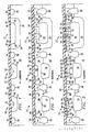
- an (n+) buried collector region 16 is masked in oxide layer 12 to limits 17 in a super-beta NPN transistor area indicated generally at 19.
- the sheet resistance of the buried collector regions 14 and 16 should be approximately 15 Ohms/square, and a preferred dopant is antimony.
- substrate 10 is subjected to a thermal diffusion step to give the respective approximate conductivity type boundaries 18 and 20 of the buried collector regions 14 and 16 as shown.
- oxide portions such as portions 22, will grow back wherever the outer surface 23 of the silicon substrate 10 has been exposed by the previous oxide removal step.
- oxide layer 12 is removed to limits 25 and an (n-) buried region 24 is implanted and thermally diffused within a vertical PNP transistor area indicated generally at 27.
- the dopant concentration used to implant buried region 24 is much less than that of collector regions 14 and 16, as using the same dopant level would overwhelm the vertical PNP collector region subsequently formed and described immediately below.
- oxide is removed within limits 34 such that the (p) type dopant implanted into region 28 will also be implanted into a plurality of deep junction isolation regions 36. Regions 36 are provided to isolate the devices from each other such that parasitic transistor devices will not be formed.
- oxide layer 40 is removed from an area within limits 54 to mask a super beta implantation step that is done with a (p) type dopant such as boron. A thermal diffusion drive-in step is then performed such that a super beta base region 56 results.
- Super beta base region 56 should have a sheet resistance of approximately 5000 Ohms/square.
- oxide layer 40 is removed within limits 56 and an (n) type dopant is implanted therein. Subsequently, oxide layer 40 is removed within limits 58 to permit the implantation of an (n) type dopant such as antimony.
- a thermal diffusion drive-in step is conducted on epitaxial layer 38 such that the (n) type dopant implanted between limits 56 and between limits 58 diffuses to create threshold adjust regions 60 and VPNP base region 62.
- Threshold adjust regions 60 are desirable to prevent parasitic PMOS transistors between (p) diffusions, such as diffused regions 46 and 48. Threshold adjust regions 60 control the junction breakdown voltage such that it can exceed the standard 45-volt operating voltage.
- oxide layer 40 is removed within limits 64 in NPN transistor area 15, super beta transistor area 19 and VPNP transistor area 27. Then, a (p) type dopant is deposited and thermally diffused to create a (p+) NPN transistor base region 66, an annular or otherwise endless (p+) super beta contact region 68, a VPNP transistor (p+) emitter region 70 and an annular or endless (p+) contact region 71 inside VPNP collector contact region 48.
- high sheet resistance resistors may be patterned by removal of certain portions of oxide layer 40 (not shown) with a subsequent oxidation and implantation to create the resistors (not shown) in layer 38.
- oxide is removed from oxide layer 40 down to the surface of the epitaxial layer 38 within limits 72 in all three device areas 15, 19 and 27 for masking the deposition of an (n) type dopant.
- the dopant thus deposited is subsequently thermally diffused to create a conventional vertical NPN emitter region 74, a super beta emitter region 76, a vertical PNP base contact region 78, collector contact regions 79 for the conventional NPN transistor and the super beta NPN transistor, and a buried region contact 81 for ohmic contact to buried region 24.
- base contact region 78 is annular or otherwise endless.
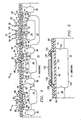
- FIGURE 4 The final steps of the preferred process are shown in FIGURE 4.
- the photoresist is stripped and a middle-level oxide layer 80 is deposited over the surface of oxide layer 40.
- Middle-level oxide layer 80 is then densified in a thermal step.
- a plurality of contact orifices 82-96 are next patterned and are etched into middle-level oxide layer 80.
- the middle-level oxide layer 80 is then reflowed into the contact orifices 82-96 to produce sloping sidewalls thereof.
- a respective orifice 98 in field oxide layer 40 is opened below each contact orifice 82-96 to expose the surface 42 of the epitaxial layer 38 therebeneath.
- Metal leads 101-118 are then deposited, patterned and etched according to conventional methodology.
- a passivating nitride layer (not shown) is preferably added thereafter to passivate the exposed surface of the completed integrated circuit.
- an orifice (not shown) is opened into oxide layer 40 and a (p) type dopant is deposited on the surface 42 of layer 38 at the same time that the (p) type deposition is performed for shallow junction isolation regions 46 and deep collector region 48 (FIGURE 2).
- a thermal diffusion step is performed that up-diffuses dopant from region 120 and down-diffuses the dopant deposited on the surface 42 of epitaxial layer 38. This combined up-diffusion and down-diffusion creates a continuous junction isolation region 122 that extends from epitaxial surface 42 into semiconductor substrate 10.
- Electrode 124 is rendered conductive by a heavy deposition of the (n) type dopant used to create emitter regions 74 and 76 and VPNP base contact region 78.
- the diffusion step by which the emitter dopant is diffused into regions 74, 76 and 78 will at the same time cause an oxide layer 126 to grow from the exposed surface of polysilicon electrode 124.
- Middle level oxide layer 80 is deposited, densified, a contact opened therein, and reflowed at the same time that these steps are performed on the middle level oxide layer 80 as shown in FIGURE 4. Finally, an outer metal electrode 132 is deposited, patterned and etched at the same time that metal contacts 101-118 are formed.
- a unified process for the fabrication of a super beta vertical NPN transistor, a vertical PNP transistor and a metal/nitride/polysilicon capacitor in a single integrated circuit has been shown and described.
- the unified process eliminates many masking steps and permits increased flexibility in circuit design.
Landscapes
- Bipolar Integrated Circuits (AREA)
- Bipolar Transistors (AREA)
- Element Separation (AREA)
Applications Claiming Priority (2)
| Application Number | Priority Date | Filing Date | Title |
|---|---|---|---|
| US20944988A | 1988-06-21 | 1988-06-21 | |
| US209449 | 1988-06-21 |
Publications (2)
| Publication Number | Publication Date |
|---|---|
| EP0347550A2 true EP0347550A2 (de) | 1989-12-27 |
| EP0347550A3 EP0347550A3 (de) | 1991-08-28 |
Family
ID=22778792
Family Applications (1)
| Application Number | Title | Priority Date | Filing Date |
|---|---|---|---|
| EP19890107210 Withdrawn EP0347550A3 (de) | 1988-06-21 | 1989-04-21 | Verfahren zur Herstellung von isolierten vertikalen und superverstärkenden Bipolar-Transistoren |
Country Status (3)
| Country | Link |
|---|---|
| EP (1) | EP0347550A3 (de) |
| JP (1) | JPH0250475A (de) |
| KR (1) | KR900001035A (de) |
Cited By (4)
| Publication number | Priority date | Publication date | Assignee | Title |
|---|---|---|---|---|
| EP0493854A1 (de) * | 1990-12-31 | 1992-07-08 | STMicroelectronics S.r.l. | Integrierte Struktur eines bipolaren Leistungstransistors und eines Wiederspannungsbipolartransistors in Emittorschaltungs- oder Halbbrückenanordnung und dies bezügliche Herstellungsverfahren |
| USRE35642E (en) * | 1987-12-22 | 1997-10-28 | Sgs-Thomson Microelectronics, S.R.L. | Integrated high-voltage bipolar power transistor and low voltage MOS power transistor structure in the emitter switching configuration and relative manufacturing process |
| USRE36311E (en) * | 1987-12-22 | 1999-09-21 | Sgs-Thomson Microelectronics, S.R.L. | Integrated high-voltage bipolar power transistor and low voltage MOS power transistor structure in the emitter switching configuration and relative manufacturing process |
| US10032868B2 (en) | 2016-09-09 | 2018-07-24 | Texas Instruments Incorporated | High performance super-beta NPN (SBNPN) |
Family Cites Families (9)
| Publication number | Priority date | Publication date | Assignee | Title |
|---|---|---|---|---|
| US3930909A (en) * | 1966-10-21 | 1976-01-06 | U.S. Philips Corporation | Method of manufacturing a semiconductor device utilizing simultaneous outdiffusion during epitaxial growth |
| FR1539042A (fr) * | 1967-06-30 | 1968-09-13 | Radiotechnique Coprim Rtc | Procédé de fabrication de transistors dans un circuit intégré |
| US3864817A (en) * | 1972-06-26 | 1975-02-11 | Sprague Electric Co | Method of making capacitor and resistor for monolithic integrated circuits |
| CA1038968A (en) * | 1974-09-19 | 1978-09-19 | Western Electric Company, Incorporated | Manufacture of complementary vertical transistors |
| JPS5365675A (en) * | 1976-11-24 | 1978-06-12 | Nec Corp | Semiconductor device |
| JPS59152658A (ja) * | 1983-02-21 | 1984-08-31 | Toko Inc | 半導体装置とその製造方法 |
| JPS62216356A (ja) * | 1986-03-18 | 1987-09-22 | Sanyo Electric Co Ltd | 半導体集積回路の製造方法 |
| JPS632380A (ja) * | 1986-06-20 | 1988-01-07 | Sanyo Electric Co Ltd | 半導体集積回路 |
| US4919970A (en) * | 1986-09-15 | 1990-04-24 | International Business Machines Corporation | Solder deposition control |
-
1989
- 1989-04-21 EP EP19890107210 patent/EP0347550A3/de not_active Withdrawn
- 1989-06-20 KR KR1019890008465A patent/KR900001035A/ko not_active Withdrawn
- 1989-06-21 JP JP1156947A patent/JPH0250475A/ja active Pending
Cited By (6)
| Publication number | Priority date | Publication date | Assignee | Title |
|---|---|---|---|---|
| USRE35642E (en) * | 1987-12-22 | 1997-10-28 | Sgs-Thomson Microelectronics, S.R.L. | Integrated high-voltage bipolar power transistor and low voltage MOS power transistor structure in the emitter switching configuration and relative manufacturing process |
| USRE36311E (en) * | 1987-12-22 | 1999-09-21 | Sgs-Thomson Microelectronics, S.R.L. | Integrated high-voltage bipolar power transistor and low voltage MOS power transistor structure in the emitter switching configuration and relative manufacturing process |
| EP0493854A1 (de) * | 1990-12-31 | 1992-07-08 | STMicroelectronics S.r.l. | Integrierte Struktur eines bipolaren Leistungstransistors und eines Wiederspannungsbipolartransistors in Emittorschaltungs- oder Halbbrückenanordnung und dies bezügliche Herstellungsverfahren |
| US5376821A (en) * | 1990-12-31 | 1994-12-27 | Sgs-Thomson Microelectronics, S.R.L. | Integrated emitter switching configuration using bipolar transistors |
| US5500551A (en) * | 1990-12-31 | 1996-03-19 | Sgs-Thomson Microelectronics, S.R.L. | Integrated emitter switching configuration using bipolar transistors |
| US10032868B2 (en) | 2016-09-09 | 2018-07-24 | Texas Instruments Incorporated | High performance super-beta NPN (SBNPN) |
Also Published As
| Publication number | Publication date |
|---|---|
| EP0347550A3 (de) | 1991-08-28 |
| KR900001035A (ko) | 1990-01-31 |
| JPH0250475A (ja) | 1990-02-20 |
Similar Documents
| Publication | Publication Date | Title |
|---|---|---|
| US4939099A (en) | Process for fabricating isolated vertical bipolar and JFET transistors | |
| US5574305A (en) | Walled-emitter transistor | |
| US4910160A (en) | High voltage complementary NPN/PNP process | |
| US6365447B1 (en) | High-voltage complementary bipolar and BiCMOS technology using double expitaxial growth | |
| US6573146B2 (en) | Methods of manufacturing complementary bipolar transistors | |
| EP0729177A2 (de) | Bipolarer Transistor | |
| US4510676A (en) | Method of fabricating a lateral PNP transistor | |
| US6033947A (en) | Driving circuit for electronic semiconductor devices including at least a power transistor | |
| US4966858A (en) | Method of fabricating a lateral semiconductor structure including field plates for self-alignment | |
| US4735912A (en) | Process of fabricating a semiconductor IC device | |
| DE68906095T2 (de) | Vertikaler Bipolartransistor. | |
| US5070382A (en) | Semiconductor structure for high power integrated circuits | |
| EP0627767B1 (de) | Verfahren zur Herstellung von JFET-Transistoren und Kondensatoren | |
| EP0347550A2 (de) | Verfahren zur Herstellung von isolierten vertikalen und superverstärkenden Bipolar-Transistoren | |
| US4721682A (en) | Isolation and substrate connection for a bipolar integrated circuit | |
| US5482874A (en) | Inversion implant isolation process | |
| US6114746A (en) | Vertical PNP transistor and relative fabrication method | |
| US4197147A (en) | Method of manufacturing an integrated circuit including an analog circuit and an I2 L circuit utilizing staged diffusion techniques | |
| EP0792514B1 (de) | Herstellungsverfahren eines integrierten schaltkreises mit komplementären isolierten bipolartransistoren | |
| US4144106A (en) | Manufacture of an I2 device utilizing staged selective diffusion thru a polycrystalline mask | |
| JPH06216142A (ja) | 改良形バイポーラトランジスタ | |
| JP2000150527A (ja) | ベ―スバラスト抵抗を使用するlpnp | |
| US5693543A (en) | Method of manufacturing a semiconductor IIL device with dielectric and diffusion isolation | |
| KR940005447B1 (ko) | 반도체장치 | |
| KR100200058B1 (ko) | 반전 주입물을 분리시키는 방법 |
Legal Events
| Date | Code | Title | Description |
|---|---|---|---|
| PUAI | Public reference made under article 153(3) epc to a published international application that has entered the european phase |
Free format text: ORIGINAL CODE: 0009012 |
|
| AK | Designated contracting states |
Kind code of ref document: A2 Designated state(s): DE FR GB IT NL |
|
| PUAL | Search report despatched |
Free format text: ORIGINAL CODE: 0009013 |
|
| AK | Designated contracting states |
Kind code of ref document: A3 Designated state(s): DE FR GB IT NL |
|
| STAA | Information on the status of an ep patent application or granted ep patent |
Free format text: STATUS: THE APPLICATION IS DEEMED TO BE WITHDRAWN |
|
| 18D | Application deemed to be withdrawn |
Effective date: 19920302 |