EP0346737A2 - Champ élastique pour tiges - Google Patents
Champ élastique pour tiges Download PDFInfo
- Publication number
- EP0346737A2 EP0346737A2 EP89110222A EP89110222A EP0346737A2 EP 0346737 A2 EP0346737 A2 EP 0346737A2 EP 89110222 A EP89110222 A EP 89110222A EP 89110222 A EP89110222 A EP 89110222A EP 0346737 A2 EP0346737 A2 EP 0346737A2
- Authority
- EP
- European Patent Office
- Prior art keywords
- grid
- contact
- directions
- expansion
- needle carrier
- Prior art date
- Legal status (The legal status is an assumption and is not a legal conclusion. Google has not performed a legal analysis and makes no representation as to the accuracy of the status listed.)
- Withdrawn
Links
Images
Classifications
-
- G—PHYSICS
- G01—MEASURING; TESTING
- G01R—MEASURING ELECTRIC VARIABLES; MEASURING MAGNETIC VARIABLES
- G01R1/00—Details of instruments or arrangements of the types included in groups G01R5/00 - G01R13/00 and G01R31/00
- G01R1/02—General constructional details
- G01R1/06—Measuring leads; Measuring probes
- G01R1/067—Measuring probes
- G01R1/073—Multiple probes
Definitions
- the invention relates to a test device according to the preamble of claims 1 and 2.
- strip adapters In contrast to complete adapters, strip adapters (contact needle carriers) are understood to be adapters, the length of which is considerably greater than the width.
- the contact needle carrier (adapter) consists, for example, of several epoxy glass plates, which are common in printed circuit board technology. These plates are plastic-impregnated glass mats (filling) that are pressed together.
- Springy test contacts can be used universally in automatic test machines and test adapters for bare and populated printed circuit boards and for wiring fields using soldering or crimping technology.
- the test contact is, for example, a steel pin with a precious metal surface, which is placed on a spring and housed with it in a spring housing. With these test contacts, the test objects (printed circuit boards) are tested for continuity and insulation. To scan the contact points, the contact needle carrier is lowered. The contact needles reach contact points, which are, for example, the eyes of a printed circuit board.
- the inner layer cores of the printed circuit boards must be structured with different reserves, since the mechanical stresses in the semi-finished product must be taken into account.
- the lead depends on the semi-finished product manufacturer (various base materials) and in one direction greater than 1 and in the other direction less than 1 in relation to a finished multilayer with nominal size 1. In this state, the cores must be checked electrically. Thereby he there is the necessity that an adaptation of the contact grid of the needle field to the actual solder grid of the test object (circuit board core) is necessary.
- the invention has for its object to achieve an adaptation in the expansion of the contact grid to the actual solder grid of the test specimen (printed circuit board), so that two differently compensated needle fields are not necessary.
- the advantage of the invention is that only a compensated needle field for scanning a core is required for both directions.
- the solution according to the invention saves material (adapter) and set-up time that would be necessary to change the needle fields.
- strip adapters it can be assumed that the length is much greater than the width.
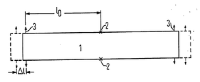
- the invention is explained with reference to the figure, which shows a strip adapter schematically in the front view.
- the needle carrier 1 is fixed in the middle 2.
- the arrows 3 each symbolize the left and right marginal needle as an example of a five-row needle field. Expands when exposed to heat the needle carrier to the shape indicated by dashed lines.
- the needles are electrically connected to the test machines (not shown).
- the underside contacts a test specimen (PCB core), which is also not shown.
- ⁇ l denotes the distance between a test needle at room temperature and a test needle at a higher temperature. This ⁇ l results at a ⁇ t, where t applies to temperature.
- the expansion ⁇ l of the contact grid due to the supply of heat is determined by a control circuit, which consists of the input variables, the desired length of the needle field, as a setpoint, the control deviation that a length sensor provides, and a disturbance variable and determines the output variable in the form of the heating power by the ⁇ t to achieve.
- ⁇ l l0 ⁇ ⁇ t
- the coefficient of expansion ⁇ of the insulation material can be both positive and negative.
- the total extent (left and right) has the amount of 2 ⁇ l (see figure).
Landscapes
- Physics & Mathematics (AREA)
- General Physics & Mathematics (AREA)
- Tests Of Electronic Circuits (AREA)
- Testing Of Short-Circuits, Discontinuities, Leakage, Or Incorrect Line Connections (AREA)
- Measuring Temperature Or Quantity Of Heat (AREA)
Applications Claiming Priority (2)
| Application Number | Priority Date | Filing Date | Title |
|---|---|---|---|
| DE3820071 | 1988-06-13 | ||
| DE3820071 | 1988-06-13 |
Publications (2)
| Publication Number | Publication Date |
|---|---|
| EP0346737A2 true EP0346737A2 (fr) | 1989-12-20 |
| EP0346737A3 EP0346737A3 (fr) | 1991-04-03 |
Family
ID=6356438
Family Applications (1)
| Application Number | Title | Priority Date | Filing Date |
|---|---|---|---|
| EP19890110222 Withdrawn EP0346737A3 (fr) | 1988-06-13 | 1989-06-06 | Champ élastique pour tiges |
Country Status (1)
| Country | Link |
|---|---|
| EP (1) | EP0346737A3 (fr) |
Family Cites Families (3)
| Publication number | Priority date | Publication date | Assignee | Title |
|---|---|---|---|---|
| DE1254224B (de) * | 1963-05-01 | 1967-11-16 | Gen Electric | Vorrichtung zur Kompensation der durch Temperaturdifferenzen bedingten Verschiebung zwischen relativ zueinander beweglichen Teilen an einer Werkzeugmaschine |
| DE1903088A1 (de) * | 1969-01-22 | 1971-01-21 | Siemens Ag | Kontaktvorrichtung |
| FR2465231A1 (fr) * | 1979-09-06 | 1981-03-20 | Thomson Csf | Tete de mesure de microcircuits, et appareil de mesure comportant une telle tete |
-
1989
- 1989-06-06 EP EP19890110222 patent/EP0346737A3/fr not_active Withdrawn
Also Published As
| Publication number | Publication date |
|---|---|
| EP0346737A3 (fr) | 1991-04-03 |
Similar Documents
| Publication | Publication Date | Title |
|---|---|---|
| DE69528421T2 (de) | Träger und Verfahren zur Herstellung einseitig mit Harz versiegelter Halbleiteranordnungen mittels des genannten Trägers | |
| DE2617190C2 (de) | Prüfeinrichtung | |
| DE4231185C2 (de) | Prüfelektrodeneinheit für gedruckte Leiterplatten sowie Prüfgerät mit einer solchen Prüfelektrodeneinheit | |
| DE69422259T2 (de) | Verbindungseinrichtung | |
| DE69109137T2 (de) | Oberflächenmontage-Verfahren und Vorrichtung. | |
| EP0263244A1 (fr) | Dispositif de test électronique pour circuits imprimés à pointes de contact disposées en trame extrêmement fine (1/20 à 1/10 de pouce) | |
| DE4203605A1 (de) | Elektrischer verbinder | |
| DE3149641C2 (fr) | ||
| DE69402049T2 (de) | Leiterplatte mit elektrischem Adaptorstift und dessen Herstellungsverfahren. | |
| EP0012319A1 (fr) | Procédé et gabarit pour la fixation de composants ayant des pattes de connexion plates sur des substrats conducteurs | |
| DE2529442C3 (de) | Verfahren und Vorrichtung zum maschinellen Einsetzen von leitenden Stiften in vorgefertigte Bohrungen einer Schaltungsplatte | |
| EP0142119B1 (fr) | Dispositif pour adapter le pas d'une grille de contact d'un appareil de contrôle de circuits imprimés | |
| DE69015854T2 (de) | Anordnung von Halbleiterbauelementen und Verfahren und Vorrichtung zur Montage von Halbleiterbauelementen. | |
| DE69201412T2 (de) | Sockel. | |
| DE2920226C2 (de) | Adapter zum Anschluß von eine Vielzahl von rasterartig verteilten Anschlußpunkten aufweisenden Prüflingen | |
| DE2640613C2 (de) | Verfahren und Vorrichtung zum Kontaktieren von Schaltungsbausteinen in eine Schichtschaltung | |
| DE10392500T5 (de) | Lottragende Artikel und Verfahren zum Zurückhalten einer Lotmasse darauf | |
| DE69102917T2 (de) | Testgerät für integrierte Schaltkreise. | |
| DE69422258T2 (de) | Verbindungseinrichtung | |
| DE10317355A1 (de) | Elektrisch leitfähige Struktur und Verfahren zum Implementieren von Schaltungsänderungen auf gedruckten Schaltungsplatinen | |
| DE3440109C2 (fr) | ||
| DE102004028067A1 (de) | Verfahren zum Anbringen einer Steckverbindung auf einem Substrat und Steckverbindung aufgebracht nach dem Verfahren | |
| DE3884736T2 (de) | Stromversorgungsleiterplatte und verfahren zu ihrer herstellung. | |
| EP1129511B1 (fr) | Composant electrique pour carte de circuits et procede pour implanter automatiquement des composants de ce type sur des cartes de circuits | |
| EP0346737A2 (fr) | Champ élastique pour tiges |
Legal Events
| Date | Code | Title | Description |
|---|---|---|---|
| PUAI | Public reference made under article 153(3) epc to a published international application that has entered the european phase |
Free format text: ORIGINAL CODE: 0009012 |
|
| AK | Designated contracting states |
Kind code of ref document: A2 Designated state(s): AT BE CH DE ES FR GB GR IT LI LU NL SE |
|
| PUAL | Search report despatched |
Free format text: ORIGINAL CODE: 0009013 |
|
| AK | Designated contracting states |
Kind code of ref document: A3 Designated state(s): AT BE CH DE ES FR GB GR IT LI LU NL SE |
|
| STAA | Information on the status of an ep patent application or granted ep patent |
Free format text: STATUS: THE APPLICATION IS DEEMED TO BE WITHDRAWN |
|
| 18D | Application deemed to be withdrawn |
Effective date: 19911004 |