EP0344752B1 - Halbleiterspeichereinrichtung mit Hochgeschwindigkeits-Lesevorrichtung - Google Patents
Halbleiterspeichereinrichtung mit Hochgeschwindigkeits-Lesevorrichtung Download PDFInfo
- Publication number
- EP0344752B1 EP0344752B1 EP89109850A EP89109850A EP0344752B1 EP 0344752 B1 EP0344752 B1 EP 0344752B1 EP 89109850 A EP89109850 A EP 89109850A EP 89109850 A EP89109850 A EP 89109850A EP 0344752 B1 EP0344752 B1 EP 0344752B1
- Authority
- EP
- European Patent Office
- Prior art keywords
- nodes
- voltage level
- pair
- data
- difference
- Prior art date
- Legal status (The legal status is an assumption and is not a legal conclusion. Google has not performed a legal analysis and makes no representation as to the accuracy of the status listed.)
- Expired - Lifetime
Links
- 239000004065 semiconductor Substances 0.000 title claims description 36
- 230000000903 blocking effect Effects 0.000 claims description 22
- 239000000758 substrate Substances 0.000 claims description 7
- 238000007599 discharging Methods 0.000 claims 2
- 230000001902 propagating effect Effects 0.000 claims 2
- 230000000694 effects Effects 0.000 claims 1
- 230000005669 field effect Effects 0.000 description 40
- 230000000295 complement effect Effects 0.000 description 14
- 238000010586 diagram Methods 0.000 description 10
- 230000003071 parasitic effect Effects 0.000 description 10
- 230000003068 static effect Effects 0.000 description 9
- 230000003321 amplification Effects 0.000 description 5
- 230000003247 decreasing effect Effects 0.000 description 5
- 238000003199 nucleic acid amplification method Methods 0.000 description 5
- 230000004913 activation Effects 0.000 description 2
- 230000006399 behavior Effects 0.000 description 2
- 230000006870 function Effects 0.000 description 2
- 238000009825 accumulation Methods 0.000 description 1
- 230000003213 activating effect Effects 0.000 description 1
- 230000008859 change Effects 0.000 description 1
- 230000008878 coupling Effects 0.000 description 1
- 238000010168 coupling process Methods 0.000 description 1
- 238000005859 coupling reaction Methods 0.000 description 1
- 238000013500 data storage Methods 0.000 description 1
- 230000007423 decrease Effects 0.000 description 1
- 230000002035 prolonged effect Effects 0.000 description 1
- 230000009467 reduction Effects 0.000 description 1
Images




Classifications
-
- G—PHYSICS
- G11—INFORMATION STORAGE
- G11C—STATIC STORES
- G11C11/00—Digital stores characterised by the use of particular electric or magnetic storage elements; Storage elements therefor
- G11C11/21—Digital stores characterised by the use of particular electric or magnetic storage elements; Storage elements therefor using electric elements
- G11C11/34—Digital stores characterised by the use of particular electric or magnetic storage elements; Storage elements therefor using electric elements using semiconductor devices
- G11C11/40—Digital stores characterised by the use of particular electric or magnetic storage elements; Storage elements therefor using electric elements using semiconductor devices using transistors
- G11C11/41—Digital stores characterised by the use of particular electric or magnetic storage elements; Storage elements therefor using electric elements using semiconductor devices using transistors forming static cells with positive feedback, i.e. cells not needing refreshing or charge regeneration, e.g. bistable multivibrator or Schmitt trigger
- G11C11/413—Auxiliary circuits, e.g. for addressing, decoding, driving, writing, sensing, timing or power reduction
- G11C11/417—Auxiliary circuits, e.g. for addressing, decoding, driving, writing, sensing, timing or power reduction for memory cells of the field-effect type
- G11C11/419—Read-write [R-W] circuits
-
- G—PHYSICS
- G11—INFORMATION STORAGE
- G11C—STATIC STORES
- G11C7/00—Arrangements for writing information into, or reading information out from, a digital store
- G11C7/06—Sense amplifiers; Associated circuits, e.g. timing or triggering circuits
- G11C7/065—Differential amplifiers of latching type
-
- G—PHYSICS
- G11—INFORMATION STORAGE
- G11C—STATIC STORES
- G11C7/00—Arrangements for writing information into, or reading information out from, a digital store
- G11C7/10—Input/output [I/O] data interface arrangements, e.g. I/O data control circuits, I/O data buffers
- G11C7/1006—Data managing, e.g. manipulating data before writing or reading out, data bus switches or control circuits therefor
Definitions
- This invention relates to a semiconductor memory device and, more particularly, to a sense amplifier circuit incorporated in the semiconductor memory device.
- FIG. 1 A typical example of the semiconductor memory device is illustrated in Fig. 1 and largely comprises a memory cell array 1 having a plurality of memory cells arranged in rows and columns, a plurality of digit line pairs 2 and 3 provided in association with the plural columns of the memory cells, respectively, a plurality of word lines 4, 5, 6 and 7 coupled to the rows of the memory cells, respectively, a row address decoder-and-buffer circuit 8 selectively activating the word lines 4 to 7, a precharging circuit 9 coupled between a source of positive voltage Vcc and the bit line pairs 2 and 3, a sense amplifier circuit 10 coupled to a data line pair 11, a bit line selector circuit 12 coupled between the bit line pairs 2 and 3 and the data line pair 11 for electrically conducting one of the bit line pairs to the data line pair, a column address decoder-and-buffer circuit 13 for shifting the bit line selector circuit 12, a data output buffer circuit 14-1 coupled to the data line pair 11, and a data input buffer circuit 14-2 also coupled to the data line pair 11.
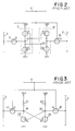
- the memory cells are of the static type, and a typical example of the static memory cell is illustrated in Fig. 2.
- the memory cell shown in Fig. 2 is constituted by a combination of two complementary inverter circuits 15 and 16 each coupled between the source of positive voltage Vcc and the ground and two n-channel type field effect transistors 17 and 18, and the two n-channel type field effect transistors 17 and 18 are simultaneously gated by a word line such as the word line 4.
- the two complementary inverter circuits 15 and 16 form in combination a flip-flop circuit, and a data bit is memorized in the static memory cell in the form of a difference in voltage level between the respective output nodes 19 and 20 of the complementary inverter circuits 15 and 16.
- a bit line pair such as the bit lines pair 2 is electrically conducted to the output nodes 19 and 20 of the complementary inverter circuits 15 and 16.
- the data bit is read out from the static memory cell to the bit line pair 2 in the read-out mode of operation, and a new data bit is written into the static memory cell in the form of the difference in voltage level between the output nodes 19 and 20 in the write-in mode of operation.
- the static memory cell shown in Fig. 2 has the two complementary inverter circuits 15 and 16, i.e., two series combinations of the p-channel type field effect transistors and the n-channel type field effect transistors for memorization of the data bit.
- the two complementary inverter circuits 15 and 16 are replaceable with two series combinations of resistors 21 and 22 and two n-channel type field effect transistors 23 and 24 as shown in Fig. 3.
- the other components are similar to those of the static memory cell shown in Fig. 2, so that they are designated by like reference numerals without detailed description.
- the row address decoder-and-buffer circuit 8 comprises a plurality of NAND gates (only one of which is shown in Fig. 1) and a plurality of NOR gates (one of which is also shown in the figure), and a multi-bit row address signal RA is supplied to the NAND gates through inverter circuits (not shown) selectively accompanying the NAND gates, so that only one NAND gate produces an output signal of the ground voltage level depending upon the bit string of the address signal.
- the NOR gates are simultaneously supplied with the complementary signal of a precharging signal from an inverter circuit 25 coupled at the input node thereof to a precharging line 26.
- the precharging line 26 propagates the precharging signal PC of an active low voltage level.
- the other input nodes of the NOR gates are coupled to the output nodes of the NAND gates, respectively, and, for this reason, one of the NOR gates allows one of the word lines to go up to the positive high voltage level Vcc in the absence of the precharging signal PC.
- the precharging circuit 9 has a plurality of p-channel type field effect transistors coupled between the source of positive voltage level Vcc and the bit lines 2 and 3, and these p-channel type field effect transistors are simultaneously gated by the precharging line 26.
- the bit line selector circuit 12 has a plurality of transfer gates associated with inverters coupled in parallel between the bit lines 2 and 3 and the data line pair 11, and these transfer gates associated with inverters selectively turn on by the function of the column address decoder-and-buffer circuit 13 for relaying only one data bit to the sense amplifier circuit 10.
- the sense amplifier circuit 10 is constituted by two complementary inverter circuits 27 and 28 and an n-channel type field effect transistor 29, and the output nodes 30 and 31 of the complementary inverter circuits 27 and 28 are respectively coupled to the data line pair 11.
- the complementary inverter circuits 27 and 28 are coupled between the source of positive voltage level Vcc and the ground in a parallel manner, and the complementary inverter circuits 27 and 28 are respectively gated by the output nodes 31 and 30, so that a small difference in voltage level on the data line pair 11 is increased by the sense amplifier circuit 10.
- the n-channel type field effect transistor 29 is provided between the two complementary inverter circuits 27 and 28 and the ground and gated by sensing signal line 32 where a sense enable signal SE of the active high voltage level appears.
- the precharging signal PC goes down to the active low voltage level at time t0, and, accordingly, the inverter circuit 25 allows the row address decoder-and-buffer circuit 8 to shift all of the word lines into the inactive low voltage level.
- the precharging circuit 9 provides conduction paths between the source of positive voltage level Vcc and all of the bit line pairs 2 and 3, so that the bit line pairs 2 and 3 as well as the data line pair 11 are fully accumulated with electric charges and, accordingly, go up to the positive high voltage level until time t1.
- the accumulation of the bit line pairs and the data line pair mean that parasitic capacitances Cb and Cd are accumulated with the electric charges.
- the sensing signal line 32 remains in the inactive low voltage level at time t1, and, for this reason, no differential amplification takes place for a data bit on the data line pair 11.
- the row address signal RA and the column address signal CA respectively reach the row address decoder-and-buffer circuit 8 and the column address decoder-and-buffer circuit 13 until time t2, and the precharging signal line 26 is recovered to the inactive high voltage level at time t2.
- the precharging circuit 9 blocks the conduction paths between the source of positive voltage level Vcc and the bit line pairs 2 and 3, and the word line 4 goes up to the positive high voltage level for allowing the data bit in the memory cell M11 to appear on the bit line pair 2.
- bit lines 2 and 2 A small difference in voltage level takes place between the bit lines 2 and is transferred to the data line pair 11, because the bit line selecting circuit 12 selectively shift the transfer gates with the inverter circuits into the on-states for providing the conduction path between the bit line pair 2 and the data line pair 11. If the data bit read out from the memory cell M11 is logic "1" level, the output nodes 19 and 20 have been in the positive high voltage level and in the ground level, respectively.
- the parasitic capacitances Cb and Cd coupled to the output node 20 are discharged from one of the data lines and one of the bit lines through the n-channel type field effect transistors 18 to the ground, and, for this reason, the out put node 31 is decreased in voltage level toward the ground level.
- the sensing signal line 32 goes up to the positive high voltage level at time t3, and, accordingly, the sense amplifier circuit 10 is activated for the differential amplification. Since a small difference in voltage level has already taken place on the data line pair 11, the output node 31 is grounded through the n-channel type field effect transistors 29. Since the output node 31 is thus further grounded, the voltage descend slightly speeds up toward the ground level, and a large difference in voltage level takes place on the data line pair 11 around time t3. The large difference in voltage level is supplied to the data output buffer circuit 14-1 and read out as the data bit stored in the memory cell M11.
- a data bit is supplied to the data input buffer circuit 14-2, and the data input data buffer circuit 14-2 provides a large difference in voltage level representative of the logic level of the data bit on the data line pair 11.
- the bit line selecting circuit 12 relays the large difference in voltage level to one of the bit line pairs, and the large difference in voltage level cause the output nodes of one of the memory cells to remain or change in voltage level for memorization of the data bit.
- the static type semiconductor memory device is increasing in the number of the memory cells, and, accordingly, each of the bit line pairs is shared by a large number of the memory cells. This tendency increases the amount of the parasitic capacitances Cb and Cd driven by the sense amplifier circuit 10. This results in that one of the output nodes of the sense amplifier circuit 10 slowly decreases in voltage level, and, accordingly, a prolonged time period is consumed for the differential amplification. Thus, a problem is encountered in the prior art semiconductor memory device in read-out operation.
- US-A 3879621 discloses sense amplifier circuit in which blocking transistors are provided to isolate data lines from the nodes of the sense amplifier during the sense operation so that the sense amplifier needs not unnecessarily discharge parasitic capacitances.
- a semiconductor memory device is fabricated on a semiconductor substrate 50 and largely comprises a memory cell array 51 arranged in rows and columns, an addressing facility, a sensing facility 52, and a temporary data storage facility.
- the semiconductor memory device is similar in arrangement to that shown in Fig. 1 except for the arrangement of the sensing facility 52 and the connection of a data input buffer circuit 53, so that corresponding circuits are denoted by like reference numerals used in Fig. 1 without any detailed description.
- the memory cell array 51 has a large number of the memory cells, however, Fig. 5 shows four memory cells labeled by M11, M12, M21 and M22.
- the bit line pairs 2 and 3 consist of the bit lines 2a and 2b and the bit lines 3a and 3b, respectively, and the data line pair 11 similarly consists of data lines 11a and 11b.
- the sensing facility comprises a sense amplifier circuit 61, blocking transistors 62 and 63 auxiliary precharging transistors 64 and 65, and the sense amplifier circuit 61 has two series combinations of p-channel field effect transistors 68 and 69 and n-channel field effect transistors 68 and 69 coupled in parallel between the source of positive voltage level Vcc and a common source node 70 and an activation transistor 71 coupled between the common source node 70 and the ground node.
- Input nodes 72 and 73 are provided between the two p-channel type field effect transistors 66 an 67 and the two n-channel type field effect transistors 68 and 69, respectively.
- the blocking transistors 62 and 63 are formed by p-channel type field effect transistors which have a threshold value of about zero.
- the gate electrodes of these p-channel type field effect transistors are coupled to the data line pair on the side of the bit line selecting circuit 12, so that the p-channel type field effect transistors serve as diodes which have the respective cathodes coupled to the bit line selecting circuit 12.
- the auxiliary precharging transistors 64 and 65 are also formed by two p-channel field effect transistors coupled between the source of positive voltage level Vcc and the input-and-output nodes 72 and 73, respectively, and these p-channel type field effect transistors are gated by the precharging signal PC.
- the data input buffer circuit 53 is coupled to the data line pair 11 between the bit line selecting circuit 12 and the blocking transistors 62 and 63.
- the complementary precharging signal of the high voltage level is supplied to the row address decoder-and-buffer circuit 8, and, accordingly, all of the word lines 4 to 7 remains in the inactive low voltage level.
- the sensing signal line 32 is in the inactive low voltage level, the sense amplifier circuit 61 does not start on the differential amplification. While the bit line pairs and so forth are precharged, the row and column address signal specifying the memory cell M11 are respectively supplied to the row address decoder-and-buffer circuit 8 and the column address decoder-and-buffer circuit 13.
- the precharging signal PC is recovered to the inactive high voltage level, and, accordingly, all of the bit line pairs 2 and 3 are blocked from the source of positive voltage level Vcc.
- the row address decoder-and-buffer circuit 8 pulls the word line 4 up to the positive high voltage level Vcc on the basis of the row address signal RA, and the column address decoder-and-buffer circuit 13 causes the bit line selecting circuit 12 to couple the bit line pair 2 to the data line pair 11 depending upon the column address signal CA.
- the memory cell M11 memorizes the data bit of logic "1"
- the bit line 2b and, accordingly, the data line 11b are discharged through the memory cell M11 to the ground, however, no variation takes place on the bit line 2a and the data line 11a.
- the parasitic capacitances Cb and Cd are too large to rapidly discharge through the small component transistors of the memory cell M11, so that only a small difference in voltage level takes place between the bit lines 2a and 2b and, accordingly, between the input-and-output nodes 72 and 73. This gradual decrements in voltage level are seen from the gentle sloops in Fig. 6.
- the blocking transistors 62 and 63 have the threshold voltage of about zero, so that the small difference between the bit lines 2a and 2b are relayed to the input-and-output nodes 72 and 73 without any substantial reduction.
- the sensing signal line 32 goes up to the active high voltage level Vcc, and the sense amplifier circuit 61 is activated to increase the small difference in voltage level between the input-and-output nodes 72 and 73. Then, the input-and-output node 73 is grounded through the n-channel type field effect transistors 69 and 71, and, accordingly, the input-and-output node 73 is slightly decreased in voltage level. This results in that the blocking transistor 63 is reversely biased to isolate the input-and-output node 73 from the data line 11b and, accordingly, from the parasitic capacitances Cb and Cd.
- the load capacitance is drastically decreased by cutting off the electrical conduction between the data line 11b and the input-and-output node 73, and, for this reason, the input-and-output node 73 reaches the ground level on the moment.
- the precharging signal PC goes down to the active low voltage level at time t30, so that the bit line pairs 2 and 3 and the data line pair 11 are precharged up again for the subsequent access.
- FIG. 7 of the drawings another semiconductor memory device embodying the present invention is similar to that shown in Fig. 5 with the exception of a blocking transistors 101 and 102 and a bit line selecting circuit 103 accompanied with an inverting circuit 104.
- component circuits and transistors are denoted by like reference numerals, and no further description is hereinbelow incorporated for the sake of simplicity.
- the data line pair 11 is dualized and dedicated to the data input buffer circuit 53 and the data output buffer circuit 14-1. Therefore, the bit line selecting circuit 103 has two sets of switching transistors coupled to the data input buffer circuit 53 and the data output buffer circuit 14-1, respectively, and one set of the switching transistors are of the p-channel type, but the other set of the switching transistors are of the n-channel type.
- the p-channel type field effect transistors of the bit line selecting circuit 103 are directly coupled to the column address decoder-and-buffer circuit 13, however, the n-channel type field effect transistors of the bit line selecting circuit 103 are coupled to the inverting circuit which in turn is coupled to the column address decoder-and-buffer circuit 13.
- the bit line selecting circuit 103 changes the switching transistors between the reading-out mode of operation and the writing mode of operation for coupling one of the bit line pairs and the data line pair 11.
- the p-channel type field effect transistors are used to couple one of the bit line pairs to the data line pair 11, so that the p-channel type field effect transistors turn off to isolate the data line pair from the bit line pair and, accordingly, from the parasitic capacitance Cb when the source node thereof reaches about 3 volts.
- the data line pair 11 is blocked from the parasitic capacitance Cb, so that the capacitive load applied to the input-and-output node 72 or 73 is reduced, and the sense amplifier circuit 61 discharges the parasitic capacitance applied to the data line 11a or 11b.
- the n-channel type field effect transistors are used to relay an input data bit from the data line pair to the selected bit line pair.
- the inverting circuit 104 is activated by a write enable signal W E and allows one of the n-channel type field effect transistors to turn on with the complementary signal of the decoded column address signal.
- the blocking transistors 101 and 102 are formed by two p-channel type, enhancement-mode field effect transistors, and the gate electrodes of these transistors are coupled to the ground node. These p-channel type field effect transistors are as large in threshold voltage level as the other component p-channel type field effect transistors such as those of the precharging circuit 9.
- the semiconductor substrate 50 where the semiconductor memory device is fabricated is biased to the positive high voltage level Vcc.
- the circuit behavior is similar to that of the semiconductor memory device shown in Fig. 5 until the sensing signal line 32 goes up to the active high voltage level Vcc. at time t21, and, for this reason, description is partially omitted for avoiding the repetition.
- the sensing signal line 32 goes up to the active high voltage level, the sense amplifier circuit 61 is activated for the differential amplification. Then, the input-and-output node 73 is grounded through the n-channel type field effect transistors 69 and 71, and the small difference between the data lines 11a and 11b is slightly increased.
- the blocking transistor 102 turns off when the source node thereof reaches about 3 volts (at time t31).
- the input-and-output node 73 is electrically isolated from the data line 11b and, accordingly, from the parasitic capacitances Cb and Cd. As a result, the input-and-output node 73 rapidly reaches the ground level and different from the input-and-output node 72 by voltage value of about Vcc.
- the time period between times t11 and t31 may be slightly longer than the time period between times t10 and t20 but is surely shorter than the time period between times t3 and t4. Then, the access time is improved by the function of the blocking transistors 101 and 102.
- the blocking transistors 101 and 102 are thus implemented by the p-channel type enhancement-mode field effect transistors with the gate electrodes coupled to the ground, and, for this reason, the blocking transistors 101 and 102 are easily feasible in comparison with the blocking transistors 62 and 63 with the threshold voltage level of about zero.
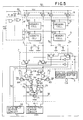
- FIG. 9 of the drawings still another semiconductor memory device is fabricated on the semiconductor substrate 50, and the semiconductor memory device is similar in circuit arrangement to that shown in Fig. 5 with the exception of a row address decoder-and-buffer circuit 201 and the precharging circuit 9.
- the row address decoder-and-buffer circuit 201 has a buffer section formed by inverter circuits 202, and the precharging circuit 9 is activated with a read enable signal RE on the precharging line 26. Then, the word line 4 goes up to the positive high voltage level Vcc at time t12, however, the circuit behavior is similar to that of the semiconductor memory device shown in Fig. 5.
- the waveforms of the essential signals are illustrated in Fig. 10.
Landscapes
- Engineering & Computer Science (AREA)
- Microelectronics & Electronic Packaging (AREA)
- Computer Hardware Design (AREA)
- Static Random-Access Memory (AREA)
- Dram (AREA)
Claims (2)
- Halbleiterspeichervorrichtung mita) einer Anzahl Speicherzellen (M11 bis M22), von denen jede ein Datenbit in Form einer Differenz des Spannungspegel speichert,b) einem Paar Datenleitungen, die ein Datenbit übertragen,c) einer Datenübertragungseinrichtung (2/3/8/12/13), die auf Adressenbits anspricht und zum Auslesen des Datenbits aus einer der Speicherzellen arbeitet und zur Schaffung einer Differenz im Spannungspegel zwischen den Datenleitungen, undd) einer Lese-Verstärkerschaltung (61) mit einem Paar Knoten (72/73), die zur Erhöhung der Differenz im Spannungspegel zwischen ihrem Paar Knoten durch Entladen einer der Knoten arbeitet,gekennzeichnet durch ein Paar Sperrtransistoren (62/63), die zwischen das Paar Datenleitungen und das Paar Knoten der Lese-Verstärkerschaltung geschaltet sind und entsprechende erste Knoten aufweisen, die mit den Datenleitungen verbunden sind, entsprechende zweite Knoten, die jeweils mit den Knoten der Leseverstärkerschaltung verbunden sind und entsprechende Gateelektroden, die entsprechend mit den ersten Knoten verbunden sind, wobei die Sperrtransistoren operativ sind zum Übertragen der Differenz des Spannungspegels zwischen den ersten Knoten an die zweiten Knoten und wobei die Sperreinrichtungen ferner operativ sind zum Isolieren eines der zweiten Knoten von der zugeordneten Datenleitung, wenn der vorgenannte eine der zweiten Knoten entladen wird.
- Auf einem Halbleitersubstrat hergestellte Halbleiterspeichervorrichtung mita) einer Vielzahl Speicherzellen (M11 bis M22), von denen jede ein Datenbit in Form einer Differenz im Spannungspegel speichert,b) einem Paar Datenleitungen (11a und 11b), die ein Datenbit übertragen,c) einer Datenübertragungseinrichtung (2/3/8/12/13), die abhängig ist von Adressenbits und arbeitet zum Auslesen eines Datenbits aus einer der Speicherzellen zur Schaffung einer Differenz im Spannungspegel zwischen den Datenleitungen, undd) einer Leseverstärkerschaltung (61) mit einem Paar Knoten (72/73), die arbeitet zum Erhöhen der Differenz im Spannungspegel zwischen ihrem Paar Knoten durch Entladung eines der Knoten,gekennzeichnet durch ein Paar Sperrtransistoren vom p-Kanal-Anreicherungstyp (101/102), das zwischen dem Paar Datenleitungen und dem Paar Knoten der Leseverstärkerschaltung geschaltet ist und mit entsprechenden ersten Knoten, die mit entsprechenden Datenleitungen verbunden sind, entsprechenden zweiten Knoten, die jeweils mit den Knoten der Leseverstärkerschaltung verbunden sind, und Gateelektroden, die mit einem Masseknoten verbunden sind, wobei das Halbleitersubstrat positiv vorgespannt ist, wobei die Sperrtransistoren operativ sind zum Übertragen der Differenz im Spannungspegel zwischen den ersten Knoten an die zweiten Knoten und wobei die Sperrtransistoren ferner operartiv sind zum Isolieren eines der zweiten Knoten von der zugeordneten einen der Datenleitungen aufgrund des Gate-Rückspannungseffekts, wenn der vorgenannte eine der zweiten Knoten entladen wird.
Applications Claiming Priority (2)
| Application Number | Priority Date | Filing Date | Title |
|---|---|---|---|
| JP135862/88 | 1988-06-01 | ||
| JP13586288 | 1988-06-01 |
Publications (2)
| Publication Number | Publication Date |
|---|---|
| EP0344752A1 EP0344752A1 (de) | 1989-12-06 |
| EP0344752B1 true EP0344752B1 (de) | 1993-03-10 |
Family
ID=15161501
Family Applications (1)
| Application Number | Title | Priority Date | Filing Date |
|---|---|---|---|
| EP89109850A Expired - Lifetime EP0344752B1 (de) | 1988-06-01 | 1989-05-31 | Halbleiterspeichereinrichtung mit Hochgeschwindigkeits-Lesevorrichtung |
Country Status (3)
| Country | Link |
|---|---|
| US (1) | US5058072A (de) |
| EP (1) | EP0344752B1 (de) |
| DE (1) | DE68905240T2 (de) |
Families Citing this family (22)
| Publication number | Priority date | Publication date | Assignee | Title |
|---|---|---|---|---|
| JP2938493B2 (ja) * | 1990-01-29 | 1999-08-23 | 沖電気工業株式会社 | 半導体記憶装置 |
| JPH0460984A (ja) * | 1990-06-25 | 1992-02-26 | Matsushita Electron Corp | 半導体記憶装置 |
| JP2715004B2 (ja) * | 1991-01-07 | 1998-02-16 | 三菱電機株式会社 | 半導体メモリ装置 |
| US5652723A (en) * | 1991-04-18 | 1997-07-29 | Mitsubishi Denki Kabushiki Kaisha | Semiconductor memory device |
| US5325335A (en) * | 1991-05-30 | 1994-06-28 | Integrated Device Technology, Inc. | Memories and amplifiers suitable for low voltage power supplies |
| JP2748744B2 (ja) * | 1991-10-01 | 1998-05-13 | 日本電気株式会社 | 半導体記憶装置 |
| JPH05159575A (ja) * | 1991-12-04 | 1993-06-25 | Oki Electric Ind Co Ltd | ダイナミックランダムアクセスメモリ |
| US5418911A (en) * | 1992-06-09 | 1995-05-23 | Intel Corporation | Data path switch method and apparatus that provides capacitive load isolation |
| JP2658768B2 (ja) * | 1992-10-19 | 1997-09-30 | 日本電気株式会社 | ダイナミックram |
| GB9223226D0 (en) * | 1992-11-05 | 1992-12-16 | Algotronix Ltd | Improved configurable cellular array (cal ii) |
| JP2894115B2 (ja) * | 1992-11-10 | 1999-05-24 | 松下電器産業株式会社 | カラム選択回路 |
| JP3181759B2 (ja) * | 1993-06-10 | 2001-07-03 | 富士通株式会社 | 半導体記憶装置 |
| JPH07147086A (ja) * | 1993-11-02 | 1995-06-06 | Nec Corp | ダイナミック型半導体記憶装置 |
| US5739654A (en) * | 1994-12-19 | 1998-04-14 | International Business Machines Corporation | Precision tool control system for a workpiece positioning apparatus |
| JP3537010B2 (ja) * | 1995-11-28 | 2004-06-14 | シャープ株式会社 | 半導体記憶装置 |
| GB2321734A (en) * | 1997-01-30 | 1998-08-05 | Motorola Inc | Circuit and method of latching a bit line in a non-volatile memory |
| US5999469A (en) * | 1998-03-04 | 1999-12-07 | Lsi Logic Corporation | Sense time reduction using midlevel precharge |
| US6573775B2 (en) | 2001-10-30 | 2003-06-03 | Integrated Device Technology, Inc. | Integrated circuit flip-flops that utilize master and slave latched sense amplifiers |
| US6700425B1 (en) | 2001-10-30 | 2004-03-02 | Integrated Device Technology, Inc. | Multi-phase clock generators that utilize differential signals to achieve reduced setup and hold times |
| US7061793B2 (en) * | 2004-03-19 | 2006-06-13 | International Business Machines Corporation | Apparatus and method for small signal sensing in an SRAM cell utilizing PFET access devices |
| US9836218B2 (en) * | 2014-10-03 | 2017-12-05 | Micron Technology, Inc. | Computing reduction and prefix sum operations in memory |
| US20260073977A1 (en) * | 2024-09-12 | 2026-03-12 | Northrop Grumman Systems Corporation | Energy Efficient Compute-in-Memory SRAM-C Circuit Architecture |
Citations (1)
| Publication number | Priority date | Publication date | Assignee | Title |
|---|---|---|---|---|
| US3879621A (en) * | 1973-04-18 | 1975-04-22 | Ibm | Sense amplifier |
Family Cites Families (11)
| Publication number | Priority date | Publication date | Assignee | Title |
|---|---|---|---|---|
| JPS51113545A (en) * | 1975-03-31 | 1976-10-06 | Hitachi Ltd | Memory |
| US3983543A (en) * | 1975-06-30 | 1976-09-28 | International Business Machines Corporation | Random access memory read/write buffer circuits incorporating complementary field effect transistors |
| US4163907A (en) * | 1977-09-16 | 1979-08-07 | Harris Corporation | Three logic state input buffers |
| JPS5570993A (en) * | 1978-11-24 | 1980-05-28 | Hitachi Ltd | Memory circuit |
| JPS55115729A (en) * | 1979-02-28 | 1980-09-05 | Toshiba Corp | Mos transistor circuit |
| JPS6032912B2 (ja) * | 1979-09-13 | 1985-07-31 | 株式会社東芝 | Cmosセンスアンプ回路 |
| JPS58189898A (ja) * | 1982-04-30 | 1983-11-05 | Toshiba Corp | ダイナミツク記憶装置 |
| JPH0648595B2 (ja) * | 1982-08-20 | 1994-06-22 | 株式会社東芝 | 半導体記憶装置のセンスアンプ |
| JPS5968889A (ja) * | 1982-10-08 | 1984-04-18 | Toshiba Corp | 半導体記憶装置 |
| EP0257912A3 (de) * | 1986-08-29 | 1989-08-23 | Kabushiki Kaisha Toshiba | Statische Halbleiterspeicheranordnung |
| US4800303A (en) * | 1987-05-19 | 1989-01-24 | Gazelle Microcircuits, Inc. | TTL compatible output buffer |
-
1989
- 1989-05-31 EP EP89109850A patent/EP0344752B1/de not_active Expired - Lifetime
- 1989-05-31 DE DE8989109850T patent/DE68905240T2/de not_active Expired - Fee Related
- 1989-06-01 US US07/359,907 patent/US5058072A/en not_active Expired - Lifetime
Patent Citations (1)
| Publication number | Priority date | Publication date | Assignee | Title |
|---|---|---|---|---|
| US3879621A (en) * | 1973-04-18 | 1975-04-22 | Ibm | Sense amplifier |
Also Published As
| Publication number | Publication date |
|---|---|
| DE68905240D1 (de) | 1993-04-15 |
| US5058072A (en) | 1991-10-15 |
| EP0344752A1 (de) | 1989-12-06 |
| DE68905240T2 (de) | 1993-07-15 |
Similar Documents
| Publication | Publication Date | Title |
|---|---|---|
| US5058072A (en) | Semiconductor memory device with high speed sensing facility | |
| KR100576844B1 (ko) | 반도체집적회로장치 | |
| CA1088668A (en) | Stored charge differential sense amplifier | |
| US4195357A (en) | Median spaced dummy cell layout for MOS random access memory | |
| US6212094B1 (en) | Low power SRAM memory cell having a single bit line | |
| JP2939027B2 (ja) | 半導体記憶装置 | |
| JP2573380B2 (ja) | 不揮発性半導体メモリ | |
| US4987560A (en) | Semiconductor memory device | |
| EP0373672B1 (de) | Halbleiterspeicherschaltung mit einer verbesserten Wiederherstellungssteuerschaltung | |
| EP0320556B1 (de) | Referenz-Spannungsgenerator für CMOS-Speicher | |
| US6154404A (en) | Integrated circuit memory devices having sense amplifier driver circuits therein that improve writing efficiency | |
| JPH04184785A (ja) | 半導体記憶装置 | |
| US4131951A (en) | High speed complementary MOS memory | |
| US4447892A (en) | Pre-charge for the bit lines of a random access memory | |
| WO2007051764A1 (en) | System and method for capacitive mis-match bit-line sensing | |
| US4380055A (en) | Static RAM memory cell | |
| US5200710A (en) | Current mirror amplifier circuit and method of driving the same | |
| US4610002A (en) | Dynamic memory circuit with improved noise-prevention circuit arrangement for word lines | |
| US5396469A (en) | SRAM memory requiring reduced voltage swing during write | |
| EP0166642A2 (de) | Blockunterteiltes Halbleiterspeichergerät mit unterteilten Bitzeilen | |
| EP0329182B1 (de) | Dekodierer-Pufferschaltung, die in einer Halbleiterspeichereinrichtung enthalten ist | |
| US5317536A (en) | Dual-port type semiconductor integrated memory circuit | |
| GB2380841A (en) | Content addressable memory device | |
| US5418748A (en) | Bit line load circuit for semiconductor static RAM | |
| US5208774A (en) | Semiconductor memory device with low power consumption output data selector |
Legal Events
| Date | Code | Title | Description |
|---|---|---|---|
| PUAI | Public reference made under article 153(3) epc to a published international application that has entered the european phase |
Free format text: ORIGINAL CODE: 0009012 |
|
| 17P | Request for examination filed |
Effective date: 19890531 |
|
| AK | Designated contracting states |
Kind code of ref document: A1 Designated state(s): DE FR GB |
|
| 17Q | First examination report despatched |
Effective date: 19910816 |
|
| GRAA | (expected) grant |
Free format text: ORIGINAL CODE: 0009210 |
|
| AK | Designated contracting states |
Kind code of ref document: B1 Designated state(s): DE FR GB |
|
| REF | Corresponds to: |
Ref document number: 68905240 Country of ref document: DE Date of ref document: 19930415 |
|
| ET | Fr: translation filed | ||
| PLBE | No opposition filed within time limit |
Free format text: ORIGINAL CODE: 0009261 |
|
| STAA | Information on the status of an ep patent application or granted ep patent |
Free format text: STATUS: NO OPPOSITION FILED WITHIN TIME LIMIT |
|
| 26N | No opposition filed | ||
| REG | Reference to a national code |
Ref country code: GB Ref legal event code: IF02 |
|
| PGFP | Annual fee paid to national office [announced via postgrant information from national office to epo] |
Ref country code: FR Payment date: 20020508 Year of fee payment: 14 |
|
| PGFP | Annual fee paid to national office [announced via postgrant information from national office to epo] |
Ref country code: GB Payment date: 20020529 Year of fee payment: 14 |
|
| PGFP | Annual fee paid to national office [announced via postgrant information from national office to epo] |
Ref country code: DE Payment date: 20020610 Year of fee payment: 14 |
|
| PG25 | Lapsed in a contracting state [announced via postgrant information from national office to epo] |
Ref country code: GB Free format text: LAPSE BECAUSE OF NON-PAYMENT OF DUE FEES Effective date: 20030531 |
|
| PG25 | Lapsed in a contracting state [announced via postgrant information from national office to epo] |
Ref country code: DE Free format text: LAPSE BECAUSE OF NON-PAYMENT OF DUE FEES Effective date: 20031202 |
|
| GBPC | Gb: european patent ceased through non-payment of renewal fee |
Effective date: 20030531 |
|
| PG25 | Lapsed in a contracting state [announced via postgrant information from national office to epo] |
Ref country code: FR Free format text: LAPSE BECAUSE OF NON-PAYMENT OF DUE FEES Effective date: 20040130 |
|
| REG | Reference to a national code |
Ref country code: FR Ref legal event code: ST |