EP0342736B1 - Phasenverriegelte Schleifenschaltung sowie Bitdetektorschaltung mit einer derartigen phasenverriegelten Schleifenschaltung - Google Patents
Phasenverriegelte Schleifenschaltung sowie Bitdetektorschaltung mit einer derartigen phasenverriegelten Schleifenschaltung Download PDFInfo
- Publication number
- EP0342736B1 EP0342736B1 EP89201181A EP89201181A EP0342736B1 EP 0342736 B1 EP0342736 B1 EP 0342736B1 EP 89201181 A EP89201181 A EP 89201181A EP 89201181 A EP89201181 A EP 89201181A EP 0342736 B1 EP0342736 B1 EP 0342736B1
- Authority
- EP
- European Patent Office
- Prior art keywords
- phase
- value
- circuit
- bit
- signal
- Prior art date
- Legal status (The legal status is an assumption and is not a legal conclusion. Google has not performed a legal analysis and makes no representation as to the accuracy of the status listed.)
- Expired - Lifetime
Links
- 238000001514 detection method Methods 0.000 title claims description 52
- 230000008859 change Effects 0.000 claims description 25
- 238000005070 sampling Methods 0.000 claims description 21
- 230000006870 function Effects 0.000 claims description 19
- 230000000737 periodic effect Effects 0.000 claims description 13
- 238000012886 linear function Methods 0.000 claims description 3
- 230000008901 benefit Effects 0.000 description 5
- 230000035945 sensitivity Effects 0.000 description 5
- 230000001419 dependent effect Effects 0.000 description 4
- 230000006978 adaptation Effects 0.000 description 2
- 230000006399 behavior Effects 0.000 description 2
- 230000008054 signal transmission Effects 0.000 description 2
- 230000009471 action Effects 0.000 description 1
- 230000005540 biological transmission Effects 0.000 description 1
- 230000003111 delayed effect Effects 0.000 description 1
- 238000000034 method Methods 0.000 description 1
- 230000010363 phase shift Effects 0.000 description 1
- 230000008569 process Effects 0.000 description 1
- 230000004044 response Effects 0.000 description 1
Images


Classifications
-
- G—PHYSICS
- G11—INFORMATION STORAGE
- G11B—INFORMATION STORAGE BASED ON RELATIVE MOVEMENT BETWEEN RECORD CARRIER AND TRANSDUCER
- G11B20/00—Signal processing not specific to the method of recording or reproducing; Circuits therefor
- G11B20/10—Digital recording or reproducing
-
- H—ELECTRICITY
- H03—ELECTRONIC CIRCUITRY
- H03L—AUTOMATIC CONTROL, STARTING, SYNCHRONISATION OR STABILISATION OF GENERATORS OF ELECTRONIC OSCILLATIONS OR PULSES
- H03L7/00—Automatic control of frequency or phase; Synchronisation
- H03L7/06—Automatic control of frequency or phase; Synchronisation using a reference signal applied to a frequency- or phase-locked loop
- H03L7/08—Details of the phase-locked loop
- H03L7/085—Details of the phase-locked loop concerning mainly the frequency- or phase-detection arrangement including the filtering or amplification of its output signal
-
- H—ELECTRICITY
- H03—ELECTRONIC CIRCUITRY
- H03L—AUTOMATIC CONTROL, STARTING, SYNCHRONISATION OR STABILISATION OF GENERATORS OF ELECTRONIC OSCILLATIONS OR PULSES
- H03L7/00—Automatic control of frequency or phase; Synchronisation
- H03L7/06—Automatic control of frequency or phase; Synchronisation using a reference signal applied to a frequency- or phase-locked loop
- H03L7/08—Details of the phase-locked loop
- H03L7/099—Details of the phase-locked loop concerning mainly the controlled oscillator of the loop
- H03L7/0991—Details of the phase-locked loop concerning mainly the controlled oscillator of the loop the oscillator being a digital oscillator, e.g. composed of a fixed oscillator followed by a variable frequency divider
-
- H—ELECTRICITY
- H04—ELECTRIC COMMUNICATION TECHNIQUE
- H04L—TRANSMISSION OF DIGITAL INFORMATION, e.g. TELEGRAPHIC COMMUNICATION
- H04L7/00—Arrangements for synchronising receiver with transmitter
- H04L7/02—Speed or phase control by the received code signals, the signals containing no special synchronisation information
- H04L7/033—Speed or phase control by the received code signals, the signals containing no special synchronisation information using the transitions of the received signal to control the phase of the synchronising-signal-generating means, e.g. using a phase-locked loop
- H04L7/0334—Processing of samples having at least three levels, e.g. soft decisions
-
- G—PHYSICS
- G11—INFORMATION STORAGE
- G11B—INFORMATION STORAGE BASED ON RELATIVE MOVEMENT BETWEEN RECORD CARRIER AND TRANSDUCER
- G11B20/00—Signal processing not specific to the method of recording or reproducing; Circuits therefor
- G11B20/10—Digital recording or reproducing
- G11B20/14—Digital recording or reproducing using self-clocking codes
- G11B20/1403—Digital recording or reproducing using self-clocking codes characterised by the use of two levels
-
- H—ELECTRICITY
- H03—ELECTRONIC CIRCUITRY
- H03L—AUTOMATIC CONTROL, STARTING, SYNCHRONISATION OR STABILISATION OF GENERATORS OF ELECTRONIC OSCILLATIONS OR PULSES
- H03L2207/00—Indexing scheme relating to automatic control of frequency or phase and to synchronisation
- H03L2207/50—All digital phase-locked loop
Definitions
- the invention relates to a phase-locked-loop circuit for deriving from a sequence of samples of a band-limited data signal the phase of the data signal at the corresponding sampling instants, which circuit comprises signal-generating means for generating in synchronism with the samples a sequence of phase values characterizing a periodic signal which varies as a substantially linear function of time between two constant limit values with a frequency which is proportional to a control value, means for deriving interpolation values from the samples by interpolation, which interpolation values indicate the relative positions with respect to the sampling instants of the instants at which the data signal crosses a detection-level, phase-comparison means for deriving from the phase values and the interpolation values a difference value which is indicative of the difference between the phase represented by the phase value and the actual phase of the data signal, and control means for controlling the signal-generating means depending on the difference value in such a way that the phase indicated by the phase value is maintained substantially equal to the actual phase of the data signal.
- the invention further relates to a bit-detection arrangement for converting the sequence of samples into a binary signal made up of bit cells, which bit-detection arrangement comprises such a phase-locked-loop circuit.
- phase-locked-loop circuit the signal-generating means for generating the sequence of phase values comprise a discrete-time oscillator, comprising a digital summing circuit having a limited summing range, the phase value stored in the summing circuit being adapted by means of the control value.
- the range of the summing circuit corresponds to 360° and the control value is constant and corresponds to 180°.
- the sampling rate is substantially equal to twice the bit rate of the data signal, so that the periodic signal characterized by the phase value has a frequency substantially equal to the bit rate.
- phase of the data signal at the instants of crossing of the detection-level is known (zero)
- the difference between the actual phase and the phase represented by the phase value can be determined after every detection-level crossing.
- the phase value is adapted depending on this difference in such a way that after adaptation the phase represented by the phase value substantially corresponds to the actual phase.
- the periodic signal characterized by the phase values and the data signal are locked in phase, so that at the sampling instants between the detection-level crossings the phase value supplied by the discrete-time oscillator is always representative of the phase of the data signal.
- a bit-detection circuit detects a bit having a logic value dictated by the sign of the last sample.
- the said phase-locked-loop circuit and bit-detection circuit can be constructed entirely by means of digital elements, which has the advantage that these circuits together with the digital circuits for processing the information, for example decoding circuits and error-correction circuits, can be integrated simply on one chip.
- the known circuits have the disadvantage that for a reliable bit detection the bit rate should be substantially equal to half the sampling rate. If the bit rate deviates from this value the phase shift between two successive samples no longer corresponds to 180°, so that the phase as represented by the phase value will deviate increasingly from the actual phase as the time interval between successive detection-level crossing increases, which may lead to erroneous bit detections.
- phase-comparison means are adapted to determine a linear combination of the phase value and the product of the interpolation value and the control value in order to derive the difference value, the control means being constructed to adapt the control value depending on the linear combination thus determined.
- the frequency of the periodic function characterized by the phase value is always maintained equal to the bit rate.
- the sensitivity of the phase-comparison means is independent of the bit rate, so that the control characteristic of the phase-locked-loop is also bit-rate independent, which enables the control characteristic of the phase-locked-loop to be optimised for a large range of bit rates.
- European Patent Application EP 0241974 describes a digital phase-locked-loop circuit in which the frequency of the function characterized by the phase values is also maintained equal to the bit rate.
- the range of the discrete-time oscillator which range is defined by the limit value, is adapted.
- the number of bits required to represent the phase value is bit-rate dependent, which leads to a comparatively complex discrete-time oscillator.
- the frequency correction of the signal characterized by the phase value is inversely proportional to the detected phase difference, which results in a non-linear transfer characteristic of the phase-locked-loop.
- the sensitivity of the employed phase-comparison means is bit-rate dependent, resulting in a bit-rate dependent transfer characteristic of the phase-locked-loop. This has the disadvantage that the transfer characteristic can be optimised for only one bit rate.
- phase-locked-loop circuit significant errors may occur in the detected phase difference, which neccesitates the use of additional correction circuits.
- said European Patent Application 0,241,974 describes another circuit in which the frequency of the periodic signal characterized by the phase value is adjusted depending on the detected phase difference.
- the frequency of said periodic signal is now maintained equal to the difference in frequency between the bit rate and the sampling rate, enabling the circuit to be used only for bit rates between one time the sampling rate and two times the sampling rate.
- the phase-detection sensitivity in this circuit is also bit-rate dependent and, moreover, additional correction circuits are needed to provide a correction for erroneously phase-difference detections.
- control means comprise means for limiting the control value to values situated between a third and a fourth limit value, which limit values respectively correspond to a minimum and maximum permissible frequency of the periodic signal characterized by the phase values.
- the frequency of the signal characterized by the phase value can vary only within a limited frequency range, which reduces the likelihood of a phase lock at an undesired frequency.
- phase-locked-loop circuit perform well. However, if the frequency component in the data signal to which the phase-locked-loop circuit locks drops out temporarily, for example as a result of a fault in the signal-transmission path, the frequency of the discrete-time oscillator is found to drift away very rapidly. This has the drawback that after the fault condition has ceased the phase-locked-loop circuit requires a comparatively long time to come back into lock, which leads to an undesirable loss of information.
- a function which complies with said requirement imposed on the relationship between the corrected phase difference ⁇ F′ and the uncorrected phase difference ⁇ F is a sine function.
- the correction circuit can be realised simply by means of a digital memory in which the relevant relationship is stored as a look-up table.
- bit-detection arrangement is characterized in that the signal-generating means comprise a digital summing circuit for adapting an n-bit sum value by means of the control value in synchronism with the sampling-clock signal, the n - 1 least significant bits representing the phase values, and the bit-detection arrangement comprising means responsive to a change in logic value of the most significant bit of the sum value to generate a clock pulse of a bit-clock signal which is in synchronism with the binary signal.
- This embodiment has the advantage that the bit-clock signal is generated in a very simple and reliable manner.
- bit-detection arrangement comprises means for deriving the logic values of the bit cells from the signs of the samples at the instants at which the clock pulses of the bit clock signal are generated and means for comparing the phase value generated immediately after the detection-level crossing with the difference value and means for inverting the logic value of the associated bit cell depending on the result of the comparison.
- the logic values of the bit cells are detected in a simple manner, in such a way that erroneously detected logic values of the bit cells the detection-level crossings are corrected.
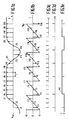
- Fig. 1a shows a sequence of equidistant samples J1,... J20 as a function of time, which samples represent a band-limited data signal Vt.
- a data signal can be obtained, for example, from a read apparatus for reading digital information recorded on a magnetic or optically readable record carrier.
- Such a signal comprises a plurality of binary bit cells which are transmitted in synchronism with a channel clock and which are representative of the information being read.
- the phase of the data signal at the sampling instants must be known.
- a digital phase-locked-loop circuit to be described in detail hereinafter, generates a sequence of phase values F1,..., F20 (see Fig. 1b), which are representative of the phase of the data signal Vt at the sampling instants.
- This sequence of phase values characterizes a periodic signal Vkl which varies as a linear function of time between two limit values - E and + E at a frequency equal to the bit rate of the data signal.
- the limit value + E corresponds to a phase of 180° and the value - E corresponds to the phase of -180°.
- the crossings of the data signal with a detection-level Vref are made to coincide substantially with the crossings of the periodic signal Vkl with the zero level indicated by a line 1.
- the digital information represented by the samples J1, ..., J20 can be recovered simply by detecting the sign of the first sample taken after the step change of the periodic signal Vkl. Depending on the sign of this sample a bit of a first a logic value (0) or of a second logic value (1) is detected (see Fig. 1c).
- a bit clock signal clo (see Fig. 1d) representing the instants at which a bit is detected can be derived from the sampling-clock signal cl (see Fig. 1c) by selecting those pulses of the sampling- clock signal cl which represent the first sampling instant after the step change of the signal Vkl.
- phase lock between the data signal Vt and the function characterized by the phase value can be achieved by determining the phase difference between the data signal Vt and the periodic signal Vk1 at every crossing of the signal Vt with the detection level Vref and subsequently adapting the frequency of the signal Vkl depending on the phase difference thus determined. How this phase difference is determined will be described in detail with reference to Fig. 2.
- a measure of the difference between the position of the crossing 30 the data signal Vt the detection-level Vref and the position of the crossing 31 of the signal Vkl with the line 1 is derived from the values of the samples J and the phase values F.
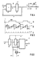
- Fig. 3 shows a bit-detection arrangement in accordance with the invention.
- This bit-detection arrangement comprises a digital phase-locked-loop circuit, comprising an interpolation circuit 2, a phase detector 3, a sequential digital filter 9 and a discrete-time oscillator 10.
- the discrete-time oscillator 10 generates the phase words F in synchronism with these samples.
- Fig. 4 shows an example of the discrete-time oscillator 10, which comprises an n-bit digital adder circuit 40 whose outputs are applied to an n-bit parallel-in parallel-out register 41 controlled by the sampling-clock signal cl. The outputs of the register are fed back to one of the inputs of the adder circuit 40. Moreover, a digital representation of I is applied to the adder circuit 40 via a bus 42. In response to every pulse of the sampling-clock signal this circuit adapts the value represented by the output signal of the register 41 by the value I. The n - 1 least significant bits on the output of the register 41 are applied to the phase detector 3. If the phase detector 3 is constructed to process numerical values of the "two's-complement" numerical system the (n - 1)th bit must be inverted by means of an inverter circuit 45 before it is applied to the phase detector 3.
- n - 1 bits are given as a function of time in Fig. 5b.
- Fig. 5c shows the sampling-clock signal as a function of time.
- Fig. 5a shows the variation in time of the logic value of the most significant bit on the output of the register 41.
- MSB logic value of the most significant bit
- the n - 1 significant bits representing the phase values F are fed out via the bus 43.
- the signal representing the logic value of the most significant bit on the output of the register 41 is fed out via a signal line 44.
- Fig. 6 shows an example of the interpolation circuit 2 for determining the ratio tf/T.
- the interpolation circuit 2 comprises two cascaded parallel-in parallel-out registers 60 and 61, which are controlled by the sampling-clock signal cl.
- the digital representations of the samples J are applied to the parallel inputs of the register 60 via a bus 62 in synchronism with the sampling-clock signal cl, so that always the digital representations of two successive samples J are available on the outputs of the registers 60 and 61.
- the outputs of the registers 60 and 61 are applied to the address inputs of a memory 63, which for every combination of two digital representations of samples of opposite sign stores the corresponding digital representations of tf/T in the formed of a look up table.
- the digital representation of tf/T of the combination applied to the address inputs is output via the parallel outputs of the memory 63 and a bus 64.
- the signal on the output of the register 60 which indicates the sign of the sample value stored is fed out via a signal line 65.
- This signal is also applied to an input of an Exclusive OR gate 66.
- the signal representing the sign of the sample value stored in the register 61 is applied to the other input of said gate 66, so that the output signal of the OR gate 66 always indicates whether a detection-level crossing has occurred between the samples J whose values are stored in the registers 60 and 61.
- the output signal of the Exclusive-OR gate 66 is fed out via a signal line 67.
- the digital representations of tf/T, I and the phase values F are applied to the phase detector via the buses 67, 43 and 42 respectively to derive the digital representation of the phase difference ⁇ F in conformity with the relationship (3).
- the phase detector comprises a multiplier 5 for multiplying the digital representation of tf/T by the digital representation of I.
- the result of this multiplication is added to the digital representation of the phase value F by means of a digital adder circuit 6.
- the result of this adding operation is loaded into a register 8 if the load-control signal of the register 8 applied via the signal line 67 indicates that a detection-level crossing has occurred.
- the output signal of the register 8 is applied to the sequential digital filter 9.
- the signal filtered by means of the filter 9 is representative of the value I applied as control value to the discrete-time oscillator 10 and to the phase detector 2 via the bus 42.
- the open-loop transfer function H1(z) of the digital phase-locked-loop circuit comprising the interpolation circuit 2, the phase detector 3, the filter 9 and the discrete-time oscillator 10 characterizes the control behaviour of the phase-locked-loop.
- the transfer functions of the filter 9 and the discrete-time oscillator 10 and the sensitivity K are all independent of the bit rate of data signal Vt, so that the control characteristic of the phase-locked-loop will not change when the bit rate changes, which has the advantage that the control behaviour can be optimized for a large range of bit rates by a suitable choice of the transfer function of the loop filter.
- the signs of the data signal Vt at the instants at which the signal Vt exhibits a step change represent the logic values of the successive bits represented by the data signal Vt. Indeed, these step changes represent the centres of the bit cells of the data signal Vt.
- the signal values of the signal Vkl and signal values of the data signal are available exclusively at the sampling instants.
- the logic values of the bits can also be derived from signs of the samples immediately following the step changes of the signal Vkl. However, the sign of this sample does not always correspond to the sign of the data signal Vt at the instant of the step change in the signal Vkl.
- the sign of the sample bearing the reference numeral 70 differs from the sign of the data signal at the instant t1 at which the step change has occurred. Indeed, between the step change and the sample 70 the data signal Vt has crossed the detection-level. Such a crossing can be detected by comparing the signal value h1 of the signal Vkl at the instant at which the data signal Vt crosses the reference level with the phase value h2 at the sampling instant immediately after the step change. If the value h2 is larger than or equal to the value h1, the sign of the sample immediately following the step change will be opposite to the sign of the data signal Vt at the instant of the step change.
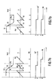
- Fig. 7b shows an example of a circuit for determining the signal Vo indicating the running value of the detected bits.
- the circuit 11a comprises a comparator circuit 80 for comparing the value h1 with the value h2.
- the input of the comparator circuit are coupled to buses 70 and 71.
- the digital representation of ⁇ F corresponding the value h1 is applied via the bus 70.
- the output signals of the register 60 which are representative of the value h2, are applied to the comparator circuit 80 via the bus 71.
- the comparator circuit 80 supplies a logic "1" signal if the value h2 is greater than h1. This signal is applied to one of the inputs of a two-input AND gate 81.
- the other input of the AND gate 81 is connected to the signal line 67, so that the AND gate 81 produces a logic "1" signal on its output after detection of a detection level crossing for which the value h2 is greater than the value h1.
- This signal is applied to an Exclusive OR gate 82.
- the logic signal representing the sign of the sample value stored in the register 60 is applied to the other input of the Exclusive OR-gate 82, the logic signal Vo′ representing the sign of the sample then being transferred to the output of the Exclusive-OR gate 82.
- Fig. 8b shows a circuit 11b for deriving the bit clock signal clo.
- the signal representing the most significant bit of the digital signal on the output of the register 41 is applied to the circuit 11b via the signal line 44.
- the logic value of this signal changes of every step change of the signal Vkl, so that by comparison of the logic values of this signal at two successive sampling instants it is possible to detect whether the signal Vk1 exhibits a step change between these two sampling instants.
- the circuit 11b comprises a flip-flop 83 controlled by the sampling-clock signal cl for delaying the signal applied via the signal line 44 by one sampling interval T.
- the delayed signal on the output of the flip-flop 83 and the signal on the signal line 44 are both applied to an Exclusive OR gate 84.
- the output signal of the gate 84 consequently always indicates whether a step change has occurred in the signal Vkl.
- the output signal of the gate 84 is applied to an input of a two-input AND gate 85.
- the sampling-clock signal cl is applied to the other input of the AND gate 85, so that after every step change of the signal Vkl one pulse of the sampling-clock signal cl is transferred to the output of the AND gate 85.
- the output signal of the AND gate 85 serves as the bit clock signal clo.
- the phase-locked-loop circuit does not lock to an incorrect frequency, for example an upper or lower harmonic of the bit rate.
- the likelihood of incorrect locking can be minimised by limiting the control value I of the discrete-time oscillator 10 to values between a minimum Imin and a maximum Imax.
- the frequency of the discrete-time oscillator 10 is directly proportional to the control value I so that by limiting I the frequency range of the discrete-time oscillator is also limited.
- Fig. 9 shows a circuit for limiting the control value I.
- the circuit can be arranged between the output of the filter 9 and the bus 42.
- the circuit comprises two comparator circuits 90 and 91 for comparing the output signal of the filter 9 with a lower limit Imin and an upper limit Imax respectively.
- the circuit further comprises a three-channel multiplex circuit 92, to which the output signals of the filter 9 and the digital representations of Imax and Imin are applied.
- the multiplex circuit 92 is controlled by the output signals of the comparator circuits 90 and 91, which signals are representative of the results of the comparisons performed by the comparator circuits 90 and 91.
- the multiplex circuit 92 is constructed in such a way that if the output signal of the comparator circuit 90 indicates that the output signal of the filter 9 is larger than Imax the digital representation of Imax is transferred to the output of the multiplex circuit 92. If the output signal of the comparator circuit 91 indicates that the output signal of the filter 9 is smaller than Imin the digital representation of Imin is transferred to the output of the multiplex circuit 92. In the other cases the output signal of the filter is transferred to the output of the multiplex circuit 92.
- the invention is not limited to the embodiment shown herein.
- a subtractor circuit can be used if the sign of the relationship between the phase values F and the control value I is opposite to the sign in the present embodiment.
- an amplifier having a predetermined gain or an attenuator having a predetermined attenuation may be arranged between the output of the discrete-time oscillator 10 and the adder circuit 6, for example, to adapt the loop gain of the phase-locked loop.
- the essential feature is that the signal value ⁇ F is a linear combination of the value F and the product of the control value I and the value tf/T.
- the digital phase-locked-loop circuit described in the foregoing performs satisfactorily provided that the data signal represented by the samples J comprises a frequency component to which the phase-locked-loop can lock.
- the value Ca representing the value of the discrete-time oscillator output at the sampling instant which directly precedes a detection-level crossing, however need not have an average value of zero.
- the discrete-time oscillator will traverse the entire range exactly N times in M samples.
- Fig. 10 gives the three successive values F1, F2 and F3 within one period of the discrete-time oscillator in the case that N is 1 and M is 3. It is evident that in the situation illustrated in Fig. 3 the output of the discrete-time oscillator has a non-zero average. If the frequency component in the data signal drops out the average value of the output signal ⁇ F will therefore also be unequal to zero, so that the frequency of the discrete-time oscillator will drift and the phase-locked-loop will act to restore the average value of the ⁇ F to zero by adaptation of the frequency of the discrete-time oscillator.
- phase detector can have such a phase characteristic that the average phase error is substantially zero.
- Fig. 12 is a graph of relationship (6).
- the correction circuit 100 can be realised very simply, for example by means of a digital memory in which the function f( ⁇ F) is stored in the form of a look-up table and whose address inputs are coupled to the output of the phase detector 3.
Landscapes
- Engineering & Computer Science (AREA)
- Signal Processing (AREA)
- Computer Networks & Wireless Communication (AREA)
- Stabilization Of Oscillater, Synchronisation, Frequency Synthesizers (AREA)
- Measurement Of Current Or Voltage (AREA)
- Signal Processing For Digital Recording And Reproducing (AREA)
- Dc Digital Transmission (AREA)
Claims (10)
n - 1
Σ f(2π k/N + ΔF) = 0
k = 1
und
k - 1
Σ f′(2π k/N + ΔF) = 0
k = 0
worin k und N ganze Zahlen sind, und f′ die Ableitung des Verhältnisses f in bezug auf ΔF ist.
Applications Claiming Priority (2)
| Application Number | Priority Date | Filing Date | Title |
|---|---|---|---|
| NL8801254 | 1988-05-16 | ||
| NL8801254 | 1988-05-16 |
Publications (2)
| Publication Number | Publication Date |
|---|---|
| EP0342736A1 EP0342736A1 (de) | 1989-11-23 |
| EP0342736B1 true EP0342736B1 (de) | 1991-08-21 |
Family
ID=19852301
Family Applications (1)
| Application Number | Title | Priority Date | Filing Date |
|---|---|---|---|
| EP89201181A Expired - Lifetime EP0342736B1 (de) | 1988-05-16 | 1989-05-10 | Phasenverriegelte Schleifenschaltung sowie Bitdetektorschaltung mit einer derartigen phasenverriegelten Schleifenschaltung |
Country Status (5)
| Country | Link |
|---|---|
| US (2) | US4912729A (de) |
| EP (1) | EP0342736B1 (de) |
| JP (1) | JP2608609B2 (de) |
| KR (1) | KR0135978B1 (de) |
| DE (1) | DE68900214D1 (de) |
Families Citing this family (44)
| Publication number | Priority date | Publication date | Assignee | Title |
|---|---|---|---|---|
| DE59009539D1 (de) * | 1990-08-29 | 1995-09-21 | Itt Ind Gmbh Deutsche | Signal-Abtrennvorrichtung. |
| US5351275A (en) * | 1991-07-15 | 1994-09-27 | National Semiconductor Corporation | Digital serial loop filter for high speed control systems |
| DE69204144T2 (de) * | 1991-11-25 | 1996-03-21 | Philips Electronics Nv | Phasenregelschleife mit Frequenzabweichungsdetektor und Decodierschaltung mit einer solchen Phasenregelschleife. |
| JP3255179B2 (ja) * | 1992-02-14 | 2002-02-12 | ソニー株式会社 | データ検出装置 |
| US5379223A (en) * | 1992-06-19 | 1995-01-03 | Alliedsignal Inc. | Inertial measurement and navigation system using digital signal processing techniques |
| US5428648A (en) * | 1992-09-18 | 1995-06-27 | Sony Corporation | Digital PLL circuit having signal edge position measurement |
| US5293369A (en) * | 1992-10-28 | 1994-03-08 | International Business Machines Corporation | Asynchronous sampling digital detector system for magnetic and optical recording channels |
| US5295128A (en) * | 1992-10-28 | 1994-03-15 | International Business Machines Corporation | Clock controller employing a discrete time control loop method for clocking data in an asynchronous channel |
| JP3693301B2 (ja) * | 1993-05-07 | 2005-09-07 | コーニンクレッカ フィリップス エレクトロニクス エヌ ヴィ | 改善されたタイミング手段を有する受信機からなる送信方式 |
| JP3390272B2 (ja) * | 1994-11-10 | 2003-03-24 | 沖電気工業株式会社 | 同期検波回路 |
| WO1997001218A1 (en) * | 1995-06-21 | 1997-01-09 | Philips Electronics N.V. | A digital radio system, a digital radio device, and a quadrature demodulator |
| KR0186138B1 (ko) * | 1995-12-23 | 1999-04-15 | 구자홍 | 디지탈 디스크의 데이타 재생장치 |
| JPH1027435A (ja) * | 1996-07-15 | 1998-01-27 | Sony Corp | 再生装置および方法 |
| WO1999017451A2 (en) | 1997-09-30 | 1999-04-08 | Koninklijke Philips Electronics N.V. | Method and device for detecting bits in a data signal |
| US6330034B1 (en) * | 1997-10-31 | 2001-12-11 | Texas Instruments Incorporated | Color phase-locked loop for video decoder |
| JP2001513306A (ja) * | 1997-12-22 | 2001-08-28 | コーニンクレッカ フィリップス エレクトロニクス エヌ ヴィ | 時間離散pll回路 |
| US7228109B2 (en) * | 2001-01-12 | 2007-06-05 | Silicon Laboratories Inc. | DC offset reduction in radio-frequency apparatus and associated methods |
| US7221921B2 (en) | 1998-05-29 | 2007-05-22 | Silicon Laboratories | Partitioning of radio-frequency apparatus |
| US7024221B2 (en) * | 2001-01-12 | 2006-04-04 | Silicon Laboratories Inc. | Notch filter for DC offset reduction in radio-frequency apparatus and associated methods |
| US7092675B2 (en) * | 1998-05-29 | 2006-08-15 | Silicon Laboratories | Apparatus and methods for generating radio frequencies in communication circuitry using multiple control signals |
| US7035607B2 (en) * | 1998-05-29 | 2006-04-25 | Silicon Laboratories Inc. | Systems and methods for providing an adjustable reference signal to RF circuitry |
| US6970717B2 (en) | 2001-01-12 | 2005-11-29 | Silicon Laboratories Inc. | Digital architecture for radio-frequency apparatus and associated methods |
| US7242912B2 (en) * | 1998-05-29 | 2007-07-10 | Silicon Laboratories Inc. | Partitioning of radio-frequency apparatus |
| US6993314B2 (en) | 1998-05-29 | 2006-01-31 | Silicon Laboratories Inc. | Apparatus for generating multiple radio frequencies in communication circuitry and associated methods |
| US6804497B2 (en) * | 2001-01-12 | 2004-10-12 | Silicon Laboratories, Inc. | Partitioned radio-frequency apparatus and associated methods |
| KR100318842B1 (ko) * | 1998-11-26 | 2002-04-22 | 윤종용 | 디지털위상제어루프에서의주파수검출방법 |
| US6366225B1 (en) * | 2000-02-14 | 2002-04-02 | Stmicroelectronics, Inc. | Circuit and method for determining the phase difference between a sample clock and a sample signal by linear approximation |
| US6903617B2 (en) | 2000-05-25 | 2005-06-07 | Silicon Laboratories Inc. | Method and apparatus for synthesizing high-frequency signals for wireless communications |
| DE10033109C2 (de) * | 2000-07-07 | 2002-06-20 | Infineon Technologies Ag | Taktsignalgenerator |
| US20030232613A1 (en) * | 2001-01-12 | 2003-12-18 | Kerth Donald A. | Quadrature signal generation in radio-frequency apparatus and associated methods |
| US7138858B2 (en) | 2001-01-12 | 2006-11-21 | Silicon Laboratories, Inc. | Apparatus and methods for output buffer circuitry with constant output power in radio-frequency circuitry |
| US7035611B2 (en) * | 2001-01-12 | 2006-04-25 | Silicon Laboratories Inc. | Apparatus and method for front-end circuitry in radio-frequency apparatus |
| US7158574B2 (en) * | 2001-01-12 | 2007-01-02 | Silicon Laboratories Inc. | Digital interface in radio-frequency apparatus and associated methods |
| US7031683B2 (en) * | 2001-01-12 | 2006-04-18 | Silicon Laboratories Inc. | Apparatus and methods for calibrating signal-processing circuitry |
| US7177610B2 (en) * | 2001-01-12 | 2007-02-13 | Silicon Laboratories Inc. | Calibrated low-noise current and voltage references and associated methods |
| US7430239B2 (en) * | 2001-11-30 | 2008-09-30 | Koninklijke Philips Electronics N.V. | Bit-detection arrangement and apparatus for reproducing information |
| EP1486079B1 (de) * | 2002-03-15 | 2015-12-30 | Silicon Laboratories Inc. | Hochfrequenzvorrichtung |
| US7124153B2 (en) | 2002-03-18 | 2006-10-17 | Genesis Microchip Inc. | Frequency converter and methods of use thereof |
| EP1634374B1 (de) | 2003-06-04 | 2006-10-04 | Koninklijke Philips Electronics N.V. | Bitdetektionsanordnung und vorrichtung zur wiedergabe von informationen |
| US7697650B2 (en) * | 2006-03-24 | 2010-04-13 | Zoran Corporation | Method and apparatus for high resolution measurement of signal timing |
| US8381074B1 (en) * | 2010-05-21 | 2013-02-19 | Lsi Corporation | Systems and methods for utilizing a centralized queue based data processing circuit |
| CN102645576B (zh) * | 2012-05-17 | 2014-11-12 | 合肥工业大学 | 一种电感电流过零点的检测装置与检测方法 |
| CN108988825B (zh) * | 2018-07-19 | 2022-08-09 | 湖北工业大学 | 一种可控硅整流双同步锁相触发控制方法 |
| KR102242169B1 (ko) | 2019-01-22 | 2021-04-19 | 상명대학교 산학협력단 | 수요 반응 기반의 전력사용량 관리 방법 |
Family Cites Families (8)
| Publication number | Priority date | Publication date | Assignee | Title |
|---|---|---|---|---|
| US3878473A (en) * | 1974-06-17 | 1975-04-15 | Ibm | Digital phase-locked loop generating signed phase values at zero crossings |
| US4423390A (en) * | 1981-01-09 | 1983-12-27 | Harris Corporation | Side lock avoidance network for PSK demodulator |
| JPS5992410A (ja) * | 1982-11-17 | 1984-05-28 | Sony Corp | デ−タ検出装置 |
| US4563650A (en) * | 1984-01-13 | 1986-01-07 | Westinghouse Electric Corp. | Power line communication receiver with dual threshold signal interrogation capability |
| US4807254A (en) * | 1985-08-09 | 1989-02-21 | Nec Corporation | Carrier wave recovery system |
| NL8600889A (nl) * | 1986-04-09 | 1987-11-02 | Philips Nv | Inrichting voor het terugwinnen van kanaalklokinformatie bij synchrone informatietransmissie en een inrichting voor het terugwinnen van de informatie voorzien van een dergelijke inrichting. |
| US4712223A (en) * | 1986-10-09 | 1987-12-08 | Rockwell International Corporation | Linear all-digital phase locked loop |
| US4749960A (en) * | 1987-04-10 | 1988-06-07 | Unisys Corporation | Long phase-locked carrier recovery loop |
-
1988
- 1988-12-15 US US07/285,131 patent/US4912729A/en not_active Expired - Lifetime
-
1989
- 1989-04-27 US US07/344,184 patent/US5067138A/en not_active Expired - Lifetime
- 1989-05-10 DE DE8989201181T patent/DE68900214D1/de not_active Expired - Lifetime
- 1989-05-10 EP EP89201181A patent/EP0342736B1/de not_active Expired - Lifetime
- 1989-05-13 KR KR1019890006398A patent/KR0135978B1/ko not_active Expired - Fee Related
- 1989-05-16 JP JP1120609A patent/JP2608609B2/ja not_active Expired - Fee Related
Also Published As
| Publication number | Publication date |
|---|---|
| JP2608609B2 (ja) | 1997-05-07 |
| JPH0222923A (ja) | 1990-01-25 |
| KR0135978B1 (ko) | 1998-05-15 |
| DE68900214D1 (de) | 1991-09-26 |
| EP0342736A1 (de) | 1989-11-23 |
| US4912729A (en) | 1990-03-27 |
| KR890017688A (ko) | 1989-12-16 |
| US5067138A (en) | 1991-11-19 |
Similar Documents
| Publication | Publication Date | Title |
|---|---|---|
| EP0342736B1 (de) | Phasenverriegelte Schleifenschaltung sowie Bitdetektorschaltung mit einer derartigen phasenverriegelten Schleifenschaltung | |
| JP3414052B2 (ja) | 位相変調信号復調方式 | |
| US5216554A (en) | Digital phase error estimator | |
| US5841323A (en) | Digital PLL using phase and frequency error calculating circuits | |
| WO2000000975A1 (en) | Pll circuit | |
| US4146841A (en) | Technique for combatting jitter in multiple phase transmission system | |
| US9793903B1 (en) | Device and method for recovering clock and data | |
| EP0277726B1 (de) | Phasenregelschleifen | |
| US6404363B1 (en) | Circuit for recovering digital clock signal and method thereof | |
| EP0241974B1 (de) | Schaltungsvorrichtung zur Regenerierung von Taktsignalen in einem Datenübertragungssystem und eine Datenrückgewinnungsanordnung mit einer solchen Vorrichtung | |
| US5272730A (en) | Digital phase-locked loop filter | |
| EP1111597B1 (de) | Vorrichtung zum Lesen von und/oder zur Aufzeichnung auf optischen Aufzeichnungsmedien | |
| US4472686A (en) | Circuit for reproducing and demodulating modulated digital signals | |
| CA1294334C (en) | Digital data separator | |
| EP0588656A2 (de) | Digitale PLL - Schaltung mit Signalflankenpositionsmessung | |
| JPS62145924A (ja) | デイジタル・フエ−ズロツクル−プ回路 | |
| US4694259A (en) | Data tracking clock recovery system having media speed variation compensation | |
| KR100398879B1 (ko) | 입력신호의 영점교차 특성을 이용한 위상오차 검출장치 | |
| US5969894A (en) | Method for detecting data encoded as state transitions in a read signal | |
| US7359474B2 (en) | Clock recovery circuit and clock-recovering filter circuit | |
| US4910517A (en) | Digital data detector | |
| EP0222132B1 (de) | Trennschaltung für digitale Daten | |
| US4415933A (en) | Carrier wave recovery circuit | |
| JPS60244124A (ja) | デジタル・フエ−ズロツクル−プ装置 | |
| EP0546851B1 (de) | Digitaler Datendetektor |
Legal Events
| Date | Code | Title | Description |
|---|---|---|---|
| PUAI | Public reference made under article 153(3) epc to a published international application that has entered the european phase |
Free format text: ORIGINAL CODE: 0009012 |
|
| AK | Designated contracting states |
Kind code of ref document: A1 Designated state(s): DE FR GB IT NL |
|
| 17P | Request for examination filed |
Effective date: 19900518 |
|
| 17Q | First examination report despatched |
Effective date: 19901008 |
|
| GRAA | (expected) grant |
Free format text: ORIGINAL CODE: 0009210 |
|
| AK | Designated contracting states |
Kind code of ref document: B1 Designated state(s): DE FR GB IT NL |
|
| PG25 | Lapsed in a contracting state [announced via postgrant information from national office to epo] |
Ref country code: NL Effective date: 19910821 |
|
| REF | Corresponds to: |
Ref document number: 68900214 Country of ref document: DE Date of ref document: 19910926 |
|
| ITF | It: translation for a ep patent filed | ||
| ET | Fr: translation filed | ||
| NLV1 | Nl: lapsed or annulled due to failure to fulfill the requirements of art. 29p and 29m of the patents act | ||
| PLBE | No opposition filed within time limit |
Free format text: ORIGINAL CODE: 0009261 |
|
| STAA | Information on the status of an ep patent application or granted ep patent |
Free format text: STATUS: NO OPPOSITION FILED WITHIN TIME LIMIT |
|
| 26N | No opposition filed | ||
| ITPR | It: changes in ownership of a european patent |
Owner name: CAMBIO RAGIONE SOCIALE;PHILIPS ELECTRONICS N.V. |
|
| REG | Reference to a national code |
Ref country code: FR Ref legal event code: CD |
|
| REG | Reference to a national code |
Ref country code: FR Ref legal event code: CD |
|
| REG | Reference to a national code |
Ref country code: GB Ref legal event code: IF02 |
|
| REG | Reference to a national code |
Ref country code: FR Ref legal event code: D6 |
|
| REG | Reference to a national code |
Ref country code: GB Ref legal event code: 746 Effective date: 20021107 |
|
| PGFP | Annual fee paid to national office [announced via postgrant information from national office to epo] |
Ref country code: FR Payment date: 20040527 Year of fee payment: 16 |
|
| PGFP | Annual fee paid to national office [announced via postgrant information from national office to epo] |
Ref country code: GB Payment date: 20040528 Year of fee payment: 16 |
|
| PGFP | Annual fee paid to national office [announced via postgrant information from national office to epo] |
Ref country code: DE Payment date: 20040714 Year of fee payment: 16 |
|
| PG25 | Lapsed in a contracting state [announced via postgrant information from national office to epo] |
Ref country code: IT Free format text: LAPSE BECAUSE OF NON-PAYMENT OF DUE FEES;WARNING: LAPSES OF ITALIAN PATENTS WITH EFFECTIVE DATE BEFORE 2007 MAY HAVE OCCURRED AT ANY TIME BEFORE 2007. THE CORRECT EFFECTIVE DATE MAY BE DIFFERENT FROM THE ONE RECORDED. Effective date: 20050510 Ref country code: GB Free format text: LAPSE BECAUSE OF NON-PAYMENT OF DUE FEES Effective date: 20050510 |
|
| PG25 | Lapsed in a contracting state [announced via postgrant information from national office to epo] |
Ref country code: DE Free format text: LAPSE BECAUSE OF NON-PAYMENT OF DUE FEES Effective date: 20051201 |
|
| GBPC | Gb: european patent ceased through non-payment of renewal fee |
Effective date: 20050510 |
|
| PG25 | Lapsed in a contracting state [announced via postgrant information from national office to epo] |
Ref country code: FR Free format text: LAPSE BECAUSE OF NON-PAYMENT OF DUE FEES Effective date: 20060131 |
|
| REG | Reference to a national code |
Ref country code: FR Ref legal event code: ST Effective date: 20060131 |