EP0341629A2 - Leiterplatte und Verfahren zum Erkennen der Position von oberflächenmontierten Bauteilen - Google Patents
Leiterplatte und Verfahren zum Erkennen der Position von oberflächenmontierten Bauteilen Download PDFInfo
- Publication number
- EP0341629A2 EP0341629A2 EP89108245A EP89108245A EP0341629A2 EP 0341629 A2 EP0341629 A2 EP 0341629A2 EP 89108245 A EP89108245 A EP 89108245A EP 89108245 A EP89108245 A EP 89108245A EP 0341629 A2 EP0341629 A2 EP 0341629A2
- Authority
- EP
- European Patent Office
- Prior art keywords
- patterns
- circuit board
- printed circuit
- position detecting
- lead connecting
- Prior art date
- Legal status (The legal status is an assumption and is not a legal conclusion. Google has not performed a legal analysis and makes no representation as to the accuracy of the status listed.)
- Granted
Links
Images


Classifications
-
- H—ELECTRICITY
- H05—ELECTRIC TECHNIQUES NOT OTHERWISE PROVIDED FOR
- H05K—PRINTED CIRCUITS; CASINGS OR CONSTRUCTIONAL DETAILS OF ELECTRIC APPARATUS; MANUFACTURE OF ASSEMBLAGES OF ELECTRICAL COMPONENTS
- H05K3/00—Apparatus or processes for manufacturing printed circuits
- H05K3/30—Assembling printed circuits with electric components, e.g. with resistors
- H05K3/32—Assembling printed circuits with electric components, e.g. with resistors electrically connecting electric components or wires to printed circuits
- H05K3/34—Assembling printed circuits with electric components, e.g. with resistors electrically connecting electric components or wires to printed circuits by soldering
-
- H—ELECTRICITY
- H05—ELECTRIC TECHNIQUES NOT OTHERWISE PROVIDED FOR
- H05K—PRINTED CIRCUITS; CASINGS OR CONSTRUCTIONAL DETAILS OF ELECTRIC APPARATUS; MANUFACTURE OF ASSEMBLAGES OF ELECTRICAL COMPONENTS
- H05K1/00—Printed circuits
- H05K1/02—Details
- H05K1/11—Printed elements for providing electric connections to or between printed circuits
- H05K1/111—Pads for surface mounting, e.g. lay-out
-
- H—ELECTRICITY
- H05—ELECTRIC TECHNIQUES NOT OTHERWISE PROVIDED FOR
- H05K—PRINTED CIRCUITS; CASINGS OR CONSTRUCTIONAL DETAILS OF ELECTRIC APPARATUS; MANUFACTURE OF ASSEMBLAGES OF ELECTRICAL COMPONENTS
- H05K1/00—Printed circuits
- H05K1/02—Details
- H05K1/0266—Marks, test patterns or identification means
- H05K1/0269—Marks, test patterns or identification means for visual or optical inspection
-
- H—ELECTRICITY
- H05—ELECTRIC TECHNIQUES NOT OTHERWISE PROVIDED FOR
- H05K—PRINTED CIRCUITS; CASINGS OR CONSTRUCTIONAL DETAILS OF ELECTRIC APPARATUS; MANUFACTURE OF ASSEMBLAGES OF ELECTRICAL COMPONENTS
- H05K13/00—Apparatus or processes specially adapted for manufacturing or adjusting assemblages of electric components
- H05K13/04—Mounting of components, e.g. of leadless components
-
- H—ELECTRICITY
- H05—ELECTRIC TECHNIQUES NOT OTHERWISE PROVIDED FOR
- H05K—PRINTED CIRCUITS; CASINGS OR CONSTRUCTIONAL DETAILS OF ELECTRIC APPARATUS; MANUFACTURE OF ASSEMBLAGES OF ELECTRICAL COMPONENTS
- H05K1/00—Printed circuits
- H05K1/02—Details
- H05K1/0266—Marks, test patterns or identification means
- H05K1/0268—Marks, test patterns or identification means for electrical inspection or testing
-
- H—ELECTRICITY
- H05—ELECTRIC TECHNIQUES NOT OTHERWISE PROVIDED FOR
- H05K—PRINTED CIRCUITS; CASINGS OR CONSTRUCTIONAL DETAILS OF ELECTRIC APPARATUS; MANUFACTURE OF ASSEMBLAGES OF ELECTRICAL COMPONENTS
- H05K2201/00—Indexing scheme relating to printed circuits covered by H05K1/00
- H05K2201/09—Shape and layout
- H05K2201/09209—Shape and layout details of conductors
- H05K2201/09654—Shape and layout details of conductors covering at least two types of conductors provided for in H05K2201/09218 - H05K2201/095
- H05K2201/09781—Dummy conductors, i.e. not used for normal transport of current; Dummy electrodes of components
-
- H—ELECTRICITY
- H05—ELECTRIC TECHNIQUES NOT OTHERWISE PROVIDED FOR
- H05K—PRINTED CIRCUITS; CASINGS OR CONSTRUCTIONAL DETAILS OF ELECTRIC APPARATUS; MANUFACTURE OF ASSEMBLAGES OF ELECTRICAL COMPONENTS
- H05K2201/00—Indexing scheme relating to printed circuits covered by H05K1/00
- H05K2201/09—Shape and layout
- H05K2201/09818—Shape or layout details not covered by a single group of H05K2201/09009 - H05K2201/09809
- H05K2201/099—Coating over pads, e.g. solder resist partly over pads
-
- H—ELECTRICITY
- H05—ELECTRIC TECHNIQUES NOT OTHERWISE PROVIDED FOR
- H05K—PRINTED CIRCUITS; CASINGS OR CONSTRUCTIONAL DETAILS OF ELECTRIC APPARATUS; MANUFACTURE OF ASSEMBLAGES OF ELECTRICAL COMPONENTS
- H05K2201/00—Indexing scheme relating to printed circuits covered by H05K1/00
- H05K2201/09—Shape and layout
- H05K2201/09818—Shape or layout details not covered by a single group of H05K2201/09009 - H05K2201/09809
- H05K2201/09909—Special local insulating pattern, e.g. as dam around component
-
- H—ELECTRICITY
- H05—ELECTRIC TECHNIQUES NOT OTHERWISE PROVIDED FOR
- H05K—PRINTED CIRCUITS; CASINGS OR CONSTRUCTIONAL DETAILS OF ELECTRIC APPARATUS; MANUFACTURE OF ASSEMBLAGES OF ELECTRICAL COMPONENTS
- H05K2201/00—Indexing scheme relating to printed circuits covered by H05K1/00
- H05K2201/09—Shape and layout
- H05K2201/09818—Shape or layout details not covered by a single group of H05K2201/09009 - H05K2201/09809
- H05K2201/09918—Optically detected marks used for aligning tool relative to the PCB, e.g. for mounting of components
-
- H—ELECTRICITY
- H05—ELECTRIC TECHNIQUES NOT OTHERWISE PROVIDED FOR
- H05K—PRINTED CIRCUITS; CASINGS OR CONSTRUCTIONAL DETAILS OF ELECTRIC APPARATUS; MANUFACTURE OF ASSEMBLAGES OF ELECTRICAL COMPONENTS
- H05K2201/00—Indexing scheme relating to printed circuits covered by H05K1/00
- H05K2201/10—Details of components or other objects attached to or integrated in a printed circuit board
- H05K2201/10613—Details of electrical connections of non-printed components, e.g. special leads
- H05K2201/10621—Components characterised by their electrical contacts
- H05K2201/10689—Leaded Integrated Circuit [IC] package, e.g. dual-in-line [DIL]
-
- H—ELECTRICITY
- H05—ELECTRIC TECHNIQUES NOT OTHERWISE PROVIDED FOR
- H05K—PRINTED CIRCUITS; CASINGS OR CONSTRUCTIONAL DETAILS OF ELECTRIC APPARATUS; MANUFACTURE OF ASSEMBLAGES OF ELECTRICAL COMPONENTS
- H05K3/00—Apparatus or processes for manufacturing printed circuits
- H05K3/30—Assembling printed circuits with electric components, e.g. with resistors
- H05K3/303—Assembling printed circuits with electric components, e.g. with resistors with surface mounted components
-
- H—ELECTRICITY
- H05—ELECTRIC TECHNIQUES NOT OTHERWISE PROVIDED FOR
- H05K—PRINTED CIRCUITS; CASINGS OR CONSTRUCTIONAL DETAILS OF ELECTRIC APPARATUS; MANUFACTURE OF ASSEMBLAGES OF ELECTRICAL COMPONENTS
- H05K3/00—Apparatus or processes for manufacturing printed circuits
- H05K3/30—Assembling printed circuits with electric components, e.g. with resistors
- H05K3/32—Assembling printed circuits with electric components, e.g. with resistors electrically connecting electric components or wires to printed circuits
- H05K3/34—Assembling printed circuits with electric components, e.g. with resistors electrically connecting electric components or wires to printed circuits by soldering
- H05K3/341—Surface mounted components
- H05K3/3421—Leaded components
-
- H—ELECTRICITY
- H05—ELECTRIC TECHNIQUES NOT OTHERWISE PROVIDED FOR
- H05K—PRINTED CIRCUITS; CASINGS OR CONSTRUCTIONAL DETAILS OF ELECTRIC APPARATUS; MANUFACTURE OF ASSEMBLAGES OF ELECTRICAL COMPONENTS
- H05K3/00—Apparatus or processes for manufacturing printed circuits
- H05K3/30—Assembling printed circuits with electric components, e.g. with resistors
- H05K3/32—Assembling printed circuits with electric components, e.g. with resistors electrically connecting electric components or wires to printed circuits
- H05K3/34—Assembling printed circuits with electric components, e.g. with resistors electrically connecting electric components or wires to printed circuits by soldering
- H05K3/3452—Solder masks
-
- Y—GENERAL TAGGING OF NEW TECHNOLOGICAL DEVELOPMENTS; GENERAL TAGGING OF CROSS-SECTIONAL TECHNOLOGIES SPANNING OVER SEVERAL SECTIONS OF THE IPC; TECHNICAL SUBJECTS COVERED BY FORMER USPC CROSS-REFERENCE ART COLLECTIONS [XRACs] AND DIGESTS
- Y02—TECHNOLOGIES OR APPLICATIONS FOR MITIGATION OR ADAPTATION AGAINST CLIMATE CHANGE
- Y02P—CLIMATE CHANGE MITIGATION TECHNOLOGIES IN THE PRODUCTION OR PROCESSING OF GOODS
- Y02P70/00—Climate change mitigation technologies in the production process for final industrial or consumer products
- Y02P70/50—Manufacturing or production processes characterised by the final manufactured product
Definitions
- the present invention relates to a printed circuit board suitable for mounting so-called surface-mounted parts such as flat pack ICs (will be termed simply FICs hereinafter), and a method of recognizing the position of a surface-mounted part on the printed circuit board.
- FICs flat pack ICs
- FICs leads have a width of about 300 ⁇ m and a lead spacing of about 350 ⁇ m.
- the number of leads is more than one hundred in some cases, and it is not easy to position, through the visual maneuver, an FIC on a printed circuit board so that all of its leads are placed on the respective conductor patterns on the board.
- An object of the present invention is to provide a printed circuit board which ensures the detection of the position and direction of conductor patterns.
- Another object of the present invention is to provide a method of recognizing the position of a surface-mounted part on the printed circuit board, capable of surely detecting the position and direction of conductor patterns.
- the printed circuit board has on its surface at least a pair of parallel rows of conductor patterns for connecting the leads of an integrated circuit, and there are provided position detecting patterns at specific positions with respect to at least two of the lead connecting conductor patterns and on lines at right angles with the rows.
- the position detecting patterns are located at specific positions at right angles with the row of lead connecting conductor patterns, and by recognizing the position of the position detecting patterns with such a visual means as an imaging tube, the position and direction of the lead connecting conductor patterns can be recognized accurately as if the lead connecting conductor patterns are detected directly.
- the method of recognizing the position of a surface-mounted part on the printed circuit board is as follows.
- the method includes a step of supporting a printed circuit board, a step of detecting positional information of detecting patterns located at specific positions with respect to at least two of lead connecting conductor patterns which belong to a row of conductor patterns and on a line at right angles with the row, and a step of calculating arithmetically the position and direction of the lead connecting conductor patterns from the positional information.
- the lead connecting conductor patterns have the application of solder and soldering paste for connecting a surface-mounted part, while the position detecting patterns do not need the application of solder and paste and therefore they provide a sufficient light reflection which enables accurate distinction from the circuit board. This allows an artificial visual means to provide reliable data on the position detecting patterns.
- the method of recognizing the position of a surface-mounted part on the printed circuit board, which bases the operation on the detection of position detecting patterns is capable of recognizing the lead connecting conductor patterns in an indirect manner at high accuracy.
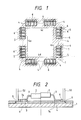
- Fig. 1 is an overall view of a printed circuit board 1, which has the formation of many lead connecting conductor patterns 4 for connecting leads 3 of an FIC, as shown in Fig. 2.
- the lead connecting conductor patterns 4 are aligned on at least a pair of rows parallel to each other (the embodiment of Fig. 1 comprises two pairs of rows including a pair 4a and 4b and another pair 4c and 4d).
- the rows 4a and 4b are parallel and the rows 4c and 4d are parallel.
- the row pair 4a and 4b and the row pair 4c and 4d are at right angles with each other.
- Formed by the lead connecting conductor patterns 4 and on lines at right angles with the rows of conductor patterns are position detecting patterns 5.
- solder resists 6 can be formed also by the print technique.
- solder layer 7a is formed on the conductor pattern 4.
- the position detecting pattern 4 is not provided with a solder layer, and the pattern surface is exposed to the atmosphere.
- Shown in the left half of Fig. 2 is the state of the lead connecting conductor pattern 4, on which the lead 3 of FIC 2 is soldered. Melted and then solidified solder 7b connects the lead 3 to the lead connecting conductor pattern 4 electrically.
- solder resist 6 which separates the position detecting pattern 5 from the lead connecting conductor pattern 4 serves as a stopper for retarding the melted solder layer 7b on the lead connecting conductor pattern 4 from flowing onto the position detecting pattern 5.
- a sufficient amount of solder can be retained on the lead connecting conductor pattern 4 for connecting the lead 3 to it, and at the same time the position detecting pattern 5 has its surface free from solder.
- This condition is advantageous for the electrical inspection of packaged printed circuit board using position detecting probes 52, because the pattern 5 provides a flat surface in a constant height, which allows a satisfactory contact between the probes 52 and position detecting patterns.
- Fig. 9 will be explained later.
- Figs. 3 and 4 show another embodiment of this invention. Shown in Fig. 3 are only lead connecting conductor patterns 4 and associated position detecting patterns 5 on one row 4b. Fig. 4 shows on the right half the state before the leads 3 of FIC 2 are soldered to the lead connecting conductor patterns 4, and shows on the left half the state after soldering. It is clearly shown in these figures that the lead connecting conductor patterns 4 and the associated position detecting pattern 5 are isolated electrically from each other. This prevents solder 7a on the lead connecting conductor pattern 4 from flowing onto the position detecting pattern 5, and a space 6a provided between the lead connecting conductor pattern 4 and position detecting pattern 5 serves as a means of retarding melted solder from flowing onto the position detecting pattern 5. The effectiveness of the retarding means is further enhanced when solder resist is placed in the space 6a.
- the position detecting pattern 5 is located on the center line 8 of the lead connecting conductor pattern 4 along its width direction (row direction) and the position detecting pattern 5 has a dimension in its width direction made smaller than the counterpart of the lead connecting conductor pattern 4. This enables an artificial visual means to detect the position of the position detecting pattern 5 which is narrower in width than the lead connecting conductor pattern 4. Since the position detecting pattern 5 is located on the center line of the lead connecting conductor pattern 4 seen in the width direction, the position of the lead connecting conductor pattern 4 can be detected accurately in an indirect manner.
- the position detecting patterns are provided only by both extremes of a row of lead connecting conductor patterns. Generally speaking, it is not necessary to provide position detecting patterns for all lead connecting conductor patterns, but the provision of at least two position detecting patterns for each row suffices for the purpose. Position detecting patterns are preferably located at symmetrical positions with respect to the center of each row.
- Fig. 5 shows the arrangement of an automatic part mounting apparatus which mounts FICs on the printed circuit board 1 (the apparatus is equipped with the part position recognition system).
- the automatic part mounting apparatus comprises two video cameras 10 and 11, an IC transporting Cartesian coordinates robot 19, a board supply unit 12 which also serves as a board support means, a flat-package supply unit 13, a roughly positioning unit 14, a vision processing unit 15 including computation means, a robot controller 16, a sequencer 17, and a console unit 18.
- the sequencer 17 is the center of control, implementing a sequential process in accordance with the predetermined sequence program.
- the robot controller 16, board supply unit 12 and roughly positioning unit 14 base their operations on the instructions issued by the sequencer 17.
- the sequencer 17 receives signals from the robot controller 16 to determine its operation.
- the robot controller 16 controls the IC transporting Cartesian coordinates robot 19 and flat-package supply unit 13.
- the vision process unit 15 receives the image signal from the video cameras 10 and 11, and implements the pattern processing for the printed circuit board 1 and FIC 2 thereby to get information for the positioning of the printed circuit board 1, the positioning of the FIC and the positioning for mounting.
- the resulting information is sent to the robot controller 16, so that the IC transporting Cartesian coordinates robot 19 and supply unit 12 are controlled, and the board supply unit 12 is controlled by the sequencer 17.
- the video camera 10 is a camera for taking the image of the suction grasp for handling the FIC and the image of the board.
- the video camera 11 is to detect the position of FIC.
- the console unit 18 includes a keyboard and CRT monitor, and the operator makes access to the vision process unit 15 and robot controller 16 through the console.
- the board supply unit 12 feeds a printed circuit board 1 to the part mount position.
- the flat-package supply unit 13 supplies an FIC from the FIC storage to the position where the robot hand takes the part.
- the roughly positioning unit 14 performs roughly positioning for the FIC.
- Fig. 6 shows the external view of the mounting apparatus, which includes the Cartesian coordinates robot 19, board supply unit 12, flat-package supply unit 13, vision process unit 15, robot controller 16 and sequencer 17, all of which are placed on a common base.
- the robot may be a horizontal articulated type which meets required positioning accuracy, and it is equipped on its hand a suction grasp for handling the FIC and the video camera for taking the image of the board.
- Another video camera 11 for detecting the position of FIC is fixed to sight upward on the base.
- steps of computation are carried out based on the positional information to determine the position and direction of the lead connecting conductor patterns.
- the algorism of computation may be exactly the same as the one disclosed in U.S. Patent No. 4,737,845, for example.
- position detecting patterns are formed only for both extremes of lead connecting conductor patterns as shown in Fig. 3, the mean value of coordinates of these position detecting patterns are calculated.
- Fig. 9 shows an example of apparatus for inspecting surface-mounted parts on a printed circuit board.
- the apparatus indicated generally by 50 comprises a support means 51 for holding a printed circuit board 1, a plurality of probes 52, a moving means 53 which brings the probes 52 in contact with the position detecting patterns 5 on the board and separates the probes 52 off the patterns, and an electrical detection means 54 which surveys the electrical continuity among probes.
- the probes 52 are exaggerated in size relative to the printed circuit board 1 in Fig. 9, they are designed to come contact with the surface of the position detecting patterns 5 of the board on which FICs are already mounted, as shown in detail in Figs. 2 and 4. Accordingly, the position detecting patterns 5 are formed on the exterior sides of the lead connecting conductor patterns 4 in this case.
- the moving means indicated generally by 53 is designed to move the probes 52 in the horizontal and vertical directions in accordance with the taught-in program.
- the electrical detection means is designed such that a specified voltage is applied between particular two probes and the current and voltage on the remaining probes are measured thereby to inspect the completed printed circuit board, with FICs being mounted, depending on whether or not the measured values meet the expected values
Landscapes
- Engineering & Computer Science (AREA)
- Microelectronics & Electronic Packaging (AREA)
- Manufacturing & Machinery (AREA)
- Electric Connection Of Electric Components To Printed Circuits (AREA)
- Supply And Installment Of Electrical Components (AREA)
- Structure Of Printed Boards (AREA)
- Length Measuring Devices With Unspecified Measuring Means (AREA)
- Testing Of Short-Circuits, Discontinuities, Leakage, Or Incorrect Line Connections (AREA)
- Testing Electric Properties And Detecting Electric Faults (AREA)
Applications Claiming Priority (2)
| Application Number | Priority Date | Filing Date | Title |
|---|---|---|---|
| JP112403/88 | 1988-05-11 | ||
| JP63112403A JPH01283993A (ja) | 1988-05-11 | 1988-05-11 | 回路プリント板、その面付け部品位置認識装置、及び面付け部品検査装置 |
Publications (3)
| Publication Number | Publication Date |
|---|---|
| EP0341629A2 true EP0341629A2 (de) | 1989-11-15 |
| EP0341629A3 EP0341629A3 (en) | 1990-12-27 |
| EP0341629B1 EP0341629B1 (de) | 1994-11-09 |
Family
ID=14585783
Family Applications (1)
| Application Number | Title | Priority Date | Filing Date |
|---|---|---|---|
| EP89108245A Expired - Lifetime EP0341629B1 (de) | 1988-05-11 | 1989-05-08 | Leiterplatte und Verfahren zum Erkennen der Position von oberflächenmontierten Bauteilen |
Country Status (5)
| Country | Link |
|---|---|
| US (1) | US5047714A (de) |
| EP (1) | EP0341629B1 (de) |
| JP (1) | JPH01283993A (de) |
| KR (1) | KR920002969B1 (de) |
| DE (1) | DE68919268T2 (de) |
Cited By (5)
| Publication number | Priority date | Publication date | Assignee | Title |
|---|---|---|---|---|
| DE4136543A1 (de) * | 1990-11-07 | 1992-05-14 | Mitsubishi Electric Corp | Schaltungsplatte und vorrichtung zum erkennen der position einer schaltungsplatte |
| EP0521338A1 (de) * | 1991-06-26 | 1993-01-07 | Siemens Nixdorf Informationssysteme Aktiengesellschaft | Verfahren und Anordnung zum Auflöten von oberflächenbefestigbaren Bausteinen auf Leiterplatten |
| EP1220597A1 (de) * | 2000-12-27 | 2002-07-03 | Alps Electric Co., Ltd. | Vorrichtung zum Untersuchen der Ausrichtung von elektronischen Komponenten |
| FR2932314A1 (fr) * | 2008-06-09 | 2009-12-11 | Valeo Equip Electr Moteur | Procede de soudure et de positionnement d'un circuit integre a montage en surface sur un substrat a plages metalliques isolees et assemblage realise par ce procede |
| WO2017040482A1 (en) * | 2015-09-02 | 2017-03-09 | 3M Innovative Properties Company | Fiducial mark for chip bonding |
Families Citing this family (9)
| Publication number | Priority date | Publication date | Assignee | Title |
|---|---|---|---|---|
| JPH0794976B2 (ja) * | 1990-05-10 | 1995-10-11 | 松下電器産業株式会社 | 電子部品のリード浮きの検出方法 |
| JPH04105582U (ja) * | 1991-02-25 | 1992-09-10 | 三菱電機株式会社 | プリント配線板 |
| US5315070A (en) * | 1991-12-02 | 1994-05-24 | Siemens Aktiengesellschaft | Printed wiring board to which solder has been applied |
| US5596282A (en) * | 1993-12-10 | 1997-01-21 | Texas Instruments Incorporated | Tester for integrated circuits |
| JP3300682B2 (ja) * | 1999-04-08 | 2002-07-08 | ファナック株式会社 | 画像処理機能を持つロボット装置 |
| US6657449B2 (en) * | 2000-12-21 | 2003-12-02 | Hansaem Digitec Co., Ltd. | Test pin unit for PCB test device and feeding device of the same |
| US20170186701A1 (en) * | 2015-12-26 | 2017-06-29 | Intel Corporation | Crack resistant electronic device package substrates |
| CN118511656A (zh) * | 2021-11-19 | 2024-08-16 | 科尔莫根公司 | 焊点检查特征 |
| KR20250054098A (ko) | 2022-08-31 | 2025-04-22 | 콜모르겐 코포레이션 | 인쇄 회로 기판 손상을 방지하는 확장된 패드 영역 |
Family Cites Families (18)
| Publication number | Priority date | Publication date | Assignee | Title |
|---|---|---|---|---|
| US3335327A (en) * | 1965-01-06 | 1967-08-08 | Augat Inc | Holder for attaching flat pack to printed circuit board |
| US3441853A (en) * | 1966-06-21 | 1969-04-29 | Signetics Corp | Plug-in integrated circuit package and carrier assembly and including a test fixture therefor |
| US4362991A (en) * | 1980-12-12 | 1982-12-07 | Burroughs Corporation | Integrated circuit test probe assembly |
| JPS57164310A (en) * | 1981-04-03 | 1982-10-08 | Hitachi Ltd | Automatic assembling device |
| JPS5821648A (ja) * | 1981-07-30 | 1983-02-08 | T Hasegawa Co Ltd | 2−アリル−2・5−ジアルコキシカルボニル−3−アルコキシカルボニルメチル−1−シクロペンタノン |
| FR2538923A1 (fr) * | 1982-12-30 | 1984-07-06 | Thomson Csf | Procede et dispositif d'alignement optique de motifs dans deux plans rapproches dans un appareil d'exposition comprenant une source de rayonnement divergent |
| DE3372673D1 (en) * | 1983-09-23 | 1987-08-27 | Ibm Deutschland | Process and device for mutually aligning objects |
| JPS6079795A (ja) * | 1983-10-06 | 1985-05-07 | キヤノン株式会社 | 両面フレキシブルプリント基板 |
| US4628464A (en) * | 1983-10-07 | 1986-12-09 | Westinghouse Electric Corp. | Robotic system for mounting electrical components |
| JPS60103700A (ja) * | 1983-11-11 | 1985-06-07 | 株式会社日立製作所 | 部品の位置決め装置 |
| US4631820A (en) * | 1984-08-23 | 1986-12-30 | Canon Kabushiki Kaisha | Mounting assembly and mounting method for an electronic component |
| EP0222072B1 (de) * | 1985-10-11 | 1993-12-15 | Hitachi, Ltd. | Verfahren zur Plazierung eines oberflächenmontierten Teiles und eine Vorrichtung dazu |
| FR2590051B1 (fr) * | 1985-11-08 | 1991-05-17 | Eurotechnique Sa | Carte comportant un composant et micromodule a contacts de flanc |
| US4733462A (en) * | 1986-06-24 | 1988-03-29 | Sony Corporation | Apparatus for positioning circuit components at predetermined positions and method therefor |
| US4761881A (en) * | 1986-09-15 | 1988-08-09 | International Business Machines Corporation | Single step solder process |
| JPS6432697A (en) * | 1987-07-28 | 1989-02-02 | Murata Manufacturing Co | Mounting structure of chip part |
| US4826441A (en) * | 1987-09-11 | 1989-05-02 | Micro Stamping Corporation | Test board connectors and method for attaching |
| JP2662870B2 (ja) * | 1988-02-10 | 1997-10-15 | 東洋通信機株式会社 | プリント配線パターン及び未ハンダ検知方法 |
-
1988
- 1988-05-11 JP JP63112403A patent/JPH01283993A/ja active Pending
-
1989
- 1989-04-27 KR KR1019890005555A patent/KR920002969B1/ko not_active Expired
- 1989-05-08 EP EP89108245A patent/EP0341629B1/de not_active Expired - Lifetime
- 1989-05-08 DE DE68919268T patent/DE68919268T2/de not_active Expired - Fee Related
- 1989-05-10 US US07/349,655 patent/US5047714A/en not_active Expired - Lifetime
Cited By (9)
| Publication number | Priority date | Publication date | Assignee | Title |
|---|---|---|---|---|
| DE4136543A1 (de) * | 1990-11-07 | 1992-05-14 | Mitsubishi Electric Corp | Schaltungsplatte und vorrichtung zum erkennen der position einer schaltungsplatte |
| DE4136543C2 (de) * | 1990-11-07 | 2003-06-26 | Mitsubishi Electric Corp | Schaltungsplatte und Verwendung einer Vorrichtung zum Erkennen der Position dieser Schaltungsplatte |
| EP0521338A1 (de) * | 1991-06-26 | 1993-01-07 | Siemens Nixdorf Informationssysteme Aktiengesellschaft | Verfahren und Anordnung zum Auflöten von oberflächenbefestigbaren Bausteinen auf Leiterplatten |
| EP1220597A1 (de) * | 2000-12-27 | 2002-07-03 | Alps Electric Co., Ltd. | Vorrichtung zum Untersuchen der Ausrichtung von elektronischen Komponenten |
| US6518512B2 (en) | 2000-12-27 | 2003-02-11 | Alps Electric Co., Ltd. | Structure for inspecting electrical component alignment |
| FR2932314A1 (fr) * | 2008-06-09 | 2009-12-11 | Valeo Equip Electr Moteur | Procede de soudure et de positionnement d'un circuit integre a montage en surface sur un substrat a plages metalliques isolees et assemblage realise par ce procede |
| EP2134147A3 (de) * | 2008-06-09 | 2011-04-13 | Valeo Equipements Electriques Moteur | Verfahren zum Auflöten und Positionieren einer integrierten Schaltung auf ein Substrat und mit diesem Verfahren hergestellte Anordnung |
| WO2017040482A1 (en) * | 2015-09-02 | 2017-03-09 | 3M Innovative Properties Company | Fiducial mark for chip bonding |
| US10438897B2 (en) | 2015-09-02 | 2019-10-08 | 3M Innovative Properties Company | Fiducial mark for chip bonding |
Also Published As
| Publication number | Publication date |
|---|---|
| EP0341629A3 (en) | 1990-12-27 |
| JPH01283993A (ja) | 1989-11-15 |
| DE68919268T2 (de) | 1995-03-23 |
| US5047714A (en) | 1991-09-10 |
| DE68919268D1 (de) | 1994-12-15 |
| EP0341629B1 (de) | 1994-11-09 |
| KR890018025A (ko) | 1989-12-18 |
| KR920002969B1 (ko) | 1992-04-11 |
Similar Documents
| Publication | Publication Date | Title |
|---|---|---|
| EP0222072B1 (de) | Verfahren zur Plazierung eines oberflächenmontierten Teiles und eine Vorrichtung dazu | |
| EP0341629B1 (de) | Leiterplatte und Verfahren zum Erkennen der Position von oberflächenmontierten Bauteilen | |
| US5768759A (en) | Method and apparatus for reflective in-flight component registration | |
| US6216341B1 (en) | Surface mounting method of electronic components | |
| US6506614B1 (en) | Method of locating and placing eye point features of a semiconductor die on a substrate | |
| JPS63180111A (ja) | 自動位置決めシステム | |
| JPH01127238A (ja) | 可動部材用の限定的再位置決め区域における位置フイードバック向上 | |
| WO2001070001A2 (en) | Pick and place machine with improved vision system | |
| CA1314085C (en) | Linear interpolation for a component placement robot | |
| EP0829192B1 (de) | Bestückungsverfahren von bauelementen auf einem substrat und bestückautomat dafür | |
| KR20010074993A (ko) | 기판 처리 방법 및 장치 | |
| US5216804A (en) | Method and device for placing a component on a printed circuit board | |
| EP0809926A1 (de) | Bestückungsautomat für bauelemente und bestückungsverfahren eines trägers | |
| JPS60140407A (ja) | チツプ部品のマウント位置決め方式 | |
| KR0165435B1 (ko) | 비젼 시스템의 카메라 취부 및 보정 방법 | |
| JP2708776B2 (ja) | 面付部品のリードピン縦曲り検出方法 | |
| JPS6286789A (ja) | 位置ずれ補正方法と面付け部品自動搭載方法 | |
| JPH10132887A (ja) | インサーキットテスタ | |
| KR0176546B1 (ko) | 로보트 장치 및 그것의 작업 위치 자동 교시 방법 | |
| JP3215754B2 (ja) | リード異常検査装置 | |
| JPH03112200A (ja) | 電子部品塔載装置 | |
| JPH0666540B2 (ja) | ケーブル組立装置 | |
| JPH0814601B2 (ja) | テープキャリヤの検査装置 | |
| JPH02281159A (ja) | 半導体検査装置 | |
| JPH0810799B2 (ja) | 電子部品の位置合せ方法 |
Legal Events
| Date | Code | Title | Description |
|---|---|---|---|
| PUAI | Public reference made under article 153(3) epc to a published international application that has entered the european phase |
Free format text: ORIGINAL CODE: 0009012 |
|
| AK | Designated contracting states |
Kind code of ref document: A2 Designated state(s): DE FR GB |
|
| PUAL | Search report despatched |
Free format text: ORIGINAL CODE: 0009013 |
|
| AK | Designated contracting states |
Kind code of ref document: A3 Designated state(s): DE FR GB |
|
| 17P | Request for examination filed |
Effective date: 19901120 |
|
| 17Q | First examination report despatched |
Effective date: 19930510 |
|
| GRAA | (expected) grant |
Free format text: ORIGINAL CODE: 0009210 |
|
| AK | Designated contracting states |
Kind code of ref document: B1 Designated state(s): DE FR GB |
|
| REF | Corresponds to: |
Ref document number: 68919268 Country of ref document: DE Date of ref document: 19941215 |
|
| ET | Fr: translation filed | ||
| PLBE | No opposition filed within time limit |
Free format text: ORIGINAL CODE: 0009261 |
|
| STAA | Information on the status of an ep patent application or granted ep patent |
Free format text: STATUS: NO OPPOSITION FILED WITHIN TIME LIMIT |
|
| 26N | No opposition filed | ||
| PGFP | Annual fee paid to national office [announced via postgrant information from national office to epo] |
Ref country code: FR Payment date: 20000418 Year of fee payment: 12 |
|
| PGFP | Annual fee paid to national office [announced via postgrant information from national office to epo] |
Ref country code: GB Payment date: 20000428 Year of fee payment: 12 |
|
| PGFP | Annual fee paid to national office [announced via postgrant information from national office to epo] |
Ref country code: DE Payment date: 20000728 Year of fee payment: 12 |
|
| PG25 | Lapsed in a contracting state [announced via postgrant information from national office to epo] |
Ref country code: GB Free format text: LAPSE BECAUSE OF NON-PAYMENT OF DUE FEES Effective date: 20010508 |
|
| GBPC | Gb: european patent ceased through non-payment of renewal fee |
Effective date: 20010508 |
|
| PG25 | Lapsed in a contracting state [announced via postgrant information from national office to epo] |
Ref country code: FR Free format text: LAPSE BECAUSE OF NON-PAYMENT OF DUE FEES Effective date: 20020131 |
|
| PG25 | Lapsed in a contracting state [announced via postgrant information from national office to epo] |
Ref country code: DE Free format text: LAPSE BECAUSE OF NON-PAYMENT OF DUE FEES Effective date: 20020301 |