EP0340866A2 - Dispositif de production d'images radiologiques au moyen de photoconducteurs - Google Patents
Dispositif de production d'images radiologiques au moyen de photoconducteurs Download PDFInfo
- Publication number
- EP0340866A2 EP0340866A2 EP89201116A EP89201116A EP0340866A2 EP 0340866 A2 EP0340866 A2 EP 0340866A2 EP 89201116 A EP89201116 A EP 89201116A EP 89201116 A EP89201116 A EP 89201116A EP 0340866 A2 EP0340866 A2 EP 0340866A2
- Authority
- EP
- European Patent Office
- Prior art keywords
- photoconductor
- ray
- exposure
- charge
- potential
- Prior art date
- Legal status (The legal status is an assumption and is not a legal conclusion. Google has not performed a legal analysis and makes no representation as to the accuracy of the status listed.)
- Granted
Links
- 230000005855 radiation Effects 0.000 claims abstract description 13
- 239000000758 substrate Substances 0.000 claims description 4
- XAGFODPZIPBFFR-UHFFFAOYSA-N aluminium Chemical compound [Al] XAGFODPZIPBFFR-UHFFFAOYSA-N 0.000 description 4
- 229910052782 aluminium Inorganic materials 0.000 description 4
- 239000002800 charge carrier Substances 0.000 description 4
- BUGBHKTXTAQXES-UHFFFAOYSA-N Selenium Chemical compound [Se] BUGBHKTXTAQXES-UHFFFAOYSA-N 0.000 description 3
- 230000000694 effects Effects 0.000 description 3
- 229910052711 selenium Inorganic materials 0.000 description 3
- 239000011669 selenium Substances 0.000 description 3
- 238000000034 method Methods 0.000 description 2
- 238000002601 radiography Methods 0.000 description 2
- 239000000523 sample Substances 0.000 description 2
- 229910052785 arsenic Inorganic materials 0.000 description 1
- RQNWIZPPADIBDY-UHFFFAOYSA-N arsenic atom Chemical compound [As] RQNWIZPPADIBDY-UHFFFAOYSA-N 0.000 description 1
- 238000005516 engineering process Methods 0.000 description 1
- 206010022000 influenza Diseases 0.000 description 1
- 239000012212 insulator Substances 0.000 description 1
- 238000004519 manufacturing process Methods 0.000 description 1
- 239000000463 material Substances 0.000 description 1
Images

Classifications
-
- G—PHYSICS
- G01—MEASURING; TESTING
- G01T—MEASUREMENT OF NUCLEAR OR X-RADIATION
- G01T1/00—Measuring X-radiation, gamma radiation, corpuscular radiation, or cosmic radiation
- G01T1/16—Measuring radiation intensity
- G01T1/26—Measuring radiation intensity with resistance detectors
-
- A—HUMAN NECESSITIES
- A61—MEDICAL OR VETERINARY SCIENCE; HYGIENE
- A61B—DIAGNOSIS; SURGERY; IDENTIFICATION
- A61B6/00—Apparatus or devices for radiation diagnosis; Apparatus or devices for radiation diagnosis combined with radiation therapy equipment
- A61B6/02—Arrangements for diagnosis sequentially in different planes; Stereoscopic radiation diagnosis
- A61B6/03—Computed tomography [CT]
- A61B6/032—Transmission computed tomography [CT]
-
- G—PHYSICS
- G01—MEASURING; TESTING
- G01R—MEASURING ELECTRIC VARIABLES; MEASURING MAGNETIC VARIABLES
- G01R29/00—Arrangements for measuring or indicating electric quantities not covered by groups G01R19/00 - G01R27/00
- G01R29/24—Arrangements for measuring quantities of charge
Definitions
- the invention relates to an arrangement for generating X-ray images by means of an X-ray radiation converting photoconductor into a charge pattern, which is charged before the X-ray image and the surface of which is scanned after the exposure to record the charge pattern.
- a corresponding arrangement is essentially known from DE-OS 29 48 660.
- An ideal photoconductor is an insulator if it is not exposed to light. It only becomes conductive during an exposure or an irradiation with X-rays, and the more so, the higher the irradiation intensity. The charge density generated by a previous charge is thus reduced at the irradiated points in accordance with the dose impinging there.
- the two-dimensional charge pattern generated in this way on the surface of the photoconductor which essentially corresponds to the spatial distribution of the X-ray dose ("latent image” or "charge image”) is converted into electrical signals by the scanning device. These are increasingly digitized, filtered and saved. They are then accessible to digital image processing.
- the object of the present invention is to design an arrangement of the type mentioned at the outset such that the extent of the artifacts described is reduced. This object is achieved in that a recharging device is provided which limits the decrease in the charge density on the surface of the photoconductor to a predetermined value during the X-ray exposure.
- the invention is based on the knowledge that the artifacts described are based on the fact that, after recharging the photoconductor following an x-ray exposure, those locations which have been particularly severely affected by x-ray radiation in the previous exposure are discharged particularly quickly, even in Dark, and that this effect is due to the fact that the photoconductor was particularly strongly discharged at the relevant points during the X-ray exposure.
- the fact that the discharge during the recording is limited to a predetermined value according to the invention prevents such a strong discharge and thus also that the photoconductor discharges particularly quickly at the relevant points after it has been recharged.
- the recharging device consists of a charge carrier source, the potential of which is selected such that the surface of the photoconductor is charged when the charge density falls below a predeterminable value.
- a preferred embodiment of such a recharging device is characterized in that the recharging device contains a corona discharge device, that a grating is arranged between the latter and the photoconductor, which covers the area of the photoconductor which can be exposed during an X-ray exposure and which approximates the potential of the photoconductor surface Grid potential corresponding value limited.
- the corona discharge device is used for charging the photoconductor before an X-ray exposure and that the voltage between the grid and the conductive substrate on which the photoconductor is arranged can be reduced to a lower value after this charging.
- a corona discharge device has one or more parallel wires which are applied to a high voltage in the operating state, so that a corona discharge results.
- a drive device is provided for generating a relative movement between the grating and the surface of the photoconductor.
- the dark discharge rate ie the change in the surface potential per unit of time in the case of an unirradiated photoconductor, is initially greatly increased after immediate charging. In the course of less Minutes, it then reduces to its normal value.
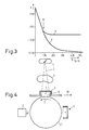
- curve a shows a typical time course of the dark discharge rate (expressed in V / min) following an X-ray exposure with a dose of 1 mGy; the time is given in minutes.
- curve c shows the dark discharge rate of the same photoconductor without prior exposure.
- a dose of the order of 1 mGy will often hit at least parts of the photoconductor because the irradiated objects in part absorb a very large proportion of the radiation.
- doses of the order of 1 to 10 ⁇ Gy hit the photoconductor, but it is inevitable that certain areas of the photoconductor will be exposed to the unattenuated direct radiation.
- FIG. 2. 1 denotes an X-ray emitter that generates an X-ray beam 2 that passes through a patient 3 and that is converted into a charge pattern by a photoconductor arrangement.
- the photoconductor arrangement consists of a 0.5 mm thick layer 5 of selenium applied to an aluminum electrode 4 and doped with 0.5% arsenic.
- the aluminum electrode is applied to a suitable insulating substrate 14.
- a grid-controlled corona discharge device is located at a short distance from the selenium layer 5.
- This comprises a housing 6, the material and wall thickness of which are selected so that the X-ray radiation is only slightly weakened. It can consist of a thin aluminum sheet or of plastic, which is metallized on one side with a thin layer.
- the conductive housing wall is grounded. The dimensions of the housing correspond to the dimensions of the photoconductor layer.
- the housing there are wires 7 arranged parallel to one another and to the surface of the photoconductor 5, which are connected to one another in an electrically conductive manner.
- the housing On its side facing the photoconductor, the housing is closed off by an electrically controllable grid 8.
- the grid has a small distance from the photoconductor (typically 0.2 to 2.0 mm) and a small mesh size (typically 0.1 to 0.5 mm).
- the surface of the photoconductor 5 is charged.
- the aluminum electrode 4 is applied to a voltage Vo of, for example, -1,750 V (compared to the housing 6).
- a positive high voltage Vs is applied to the wires 7, the amount of which is selected such that the surface of the photoconductor is charged to the potential of the grating Vg within a time of 10 to 100 ms.
- the grid potential either corresponds to ground potential (0 V) or is slightly negative, so that all charge carriers generated by the corona discharge around the wires 7 are accelerated towards the grid.
- the desired surface potential is therefore set relatively precisely on its surface, the fluctuations in the surface potential caused by the structure of the lattice-controlled corona discharge device 6 .. 8 being less than 0.1 V.
- the photoconductor 5 would discharge at the subsequent X-ray exposure at a rate that is essentially proportional to the X-ray dose rate.
- the discharge stops only when the charge on the surface of the photoconductor has been reduced, unless the X-ray tube 1 has been switched off beforehand.
- the surface potential as a function of the x-ray dose obtained in the x-ray exposure would have the typical profile shown by curve d in FIG. 3.
- the corona discharge device is not switched off in the case of an X-ray exposure, but is operated further, and only the difference Vg-Vo between grid and substrate potential is reduced, for example by operating the control grid 8 with a negative potential Vg of -900 V.
- Vg negative potential
- the control grid is then permeable to positive charge carriers, so that they reach the corresponding points on the surface of the photoconductor and compensate for the discharge current induced by the radiation.
- the surface potential as a function of the radiation dose then has the course marked by curve e in FIG. 3, which is identical to that of curve d up to a limit dose D1 of approximately 100 ⁇ Gy, but is then largely independent of the radiation dose.
- Curve b in FIG. 1 shows the time course of the dark discharge rate in the case of a photoconductor, which is recharged in accordance with curve e in FIG. 3 when the charge density or the potential on the surface falls below a limit value, so that a charge occurs at the relevant points sets a predetermined potential or a predetermined charge density. It can be seen that this limitation of the charge density or the potential on the surface significantly reduces the dark discharge effect compared to a dark discharge without recharging during the previous exposure (curve a).
- the limit dose is approximately 100 ⁇ Gy; if necessary, it can be increased to approximately 200 ⁇ Gy by increasing the electrode voltage Vo or by reducing Vg. In medical diagnostic applications, the average doses are between 1 and 10 ⁇ Gy. This generally remains mean a sufficiently large exposure latitude upwards.
- the photoconductor With the exposure technology common in projection radiography, the photoconductor is flat and has maximum dimensions of 450 x 450 mm2 square; all areas of the photoconductor are exposed simultaneously. To carry out the reloading process, a corona device is therefore required which covers the entire sector area.
- the wires 7 and the grating 8 can be imaged in an x-ray because they absorb x-rays. This image can, however, be prevented by moving the housing 6 together with the components therein by means of a drive device 9 during the x-ray exposure with a suitable frequency and amplitude (similar to an anti-scatter grid), so that the structures of these parts are blurred in the image will.
- the design of the corona device is considerably simpler if the method is used in a device for slit radiography, as is known, for example, from DE-OS 35 34 768. Such a device is shown in Fig. 4 and is briefly explained below.
- a comparatively narrow beam 2 is masked out, which only penetrates part of the examination object and exposes only a part of the photoconductor 4, 5 which is located on the surface of a drum rotating during the x-ray recording.
- the image is made in that the surface of the photoconductor 4, 5 and the object 3 on the one hand and the beam 2 on the other are moved relative to each other, as indicated by the arrows 10 and 11, so that the X-ray image on the cylindrical surface of the photoconductor 4, 5 of the entire subject 3 appears, which can be scanned and further processed digitally by means of a schematically illustrated influenza probe arrangement 12.
- the corona discharge device only has to cover the slit of the photoconductor surface, which is exposed during the x-ray exposure.
- the dimensions of the device 6..8 can therefore be significantly reduced.
- the relative movement between the photoconductor and the exposure slit prevents the structures of the corona discharge device from being imaged on the X-ray image.
- An additional movement device (such as device 9 in FIG. 2) is therefore not necessary.
- the corona discharge device 6, 7, 8 intended for recharging can, just as in the arrangement according to FIG. 2, serve to charge the photoconductor 4, 5 before the X-ray exposure. In this case, the corona discharge device 13 serving for charging and located outside the beam path can be omitted.
Landscapes
- Health & Medical Sciences (AREA)
- Life Sciences & Earth Sciences (AREA)
- Physics & Mathematics (AREA)
- Engineering & Computer Science (AREA)
- General Physics & Mathematics (AREA)
- Medical Informatics (AREA)
- Molecular Biology (AREA)
- High Energy & Nuclear Physics (AREA)
- Optics & Photonics (AREA)
- Animal Behavior & Ethology (AREA)
- Theoretical Computer Science (AREA)
- Pathology (AREA)
- Radiology & Medical Imaging (AREA)
- Biomedical Technology (AREA)
- Heart & Thoracic Surgery (AREA)
- Biophysics (AREA)
- Surgery (AREA)
- Nuclear Medicine, Radiotherapy & Molecular Imaging (AREA)
- General Health & Medical Sciences (AREA)
- Public Health (AREA)
- Veterinary Medicine (AREA)
- Pulmonology (AREA)
- Spectroscopy & Molecular Physics (AREA)
- Radiography Using Non-Light Waves (AREA)
- Apparatus For Radiation Diagnosis (AREA)
- Measurement Of Radiation (AREA)
- Control Or Security For Electrophotography (AREA)
- Transforming Light Signals Into Electric Signals (AREA)
Applications Claiming Priority (2)
| Application Number | Priority Date | Filing Date | Title |
|---|---|---|---|
| DE3815458A DE3815458A1 (de) | 1988-05-06 | 1988-05-06 | Anordnung zur erzeugung von roentgenaufnahmen mittels eines photoleiters |
| DE3815458 | 1988-05-06 |
Publications (3)
| Publication Number | Publication Date |
|---|---|
| EP0340866A2 true EP0340866A2 (fr) | 1989-11-08 |
| EP0340866A3 EP0340866A3 (fr) | 1991-01-09 |
| EP0340866B1 EP0340866B1 (fr) | 1994-08-17 |
Family
ID=6353781
Family Applications (1)
| Application Number | Title | Priority Date | Filing Date |
|---|---|---|---|
| EP89201116A Expired - Lifetime EP0340866B1 (fr) | 1988-05-06 | 1989-05-01 | Dispositif de production d'images radiologiques au moyen de photoconducteurs |
Country Status (4)
| Country | Link |
|---|---|
| US (1) | US4998266A (fr) |
| EP (1) | EP0340866B1 (fr) |
| JP (1) | JPH0222639A (fr) |
| DE (2) | DE3815458A1 (fr) |
Families Citing this family (8)
| Publication number | Priority date | Publication date | Assignee | Title |
|---|---|---|---|---|
| JP2771717B2 (ja) * | 1991-10-04 | 1998-07-02 | 富士写真フイルム株式会社 | 蓄積性蛍光体シートの除電機構 |
| US5969360A (en) * | 1997-11-26 | 1999-10-19 | Direct Radiography Corp. | Readout sequence for residual image elimination in a radiation detection panel |
| IL123006A (en) | 1998-01-20 | 2005-12-18 | Edge Medical Devices Ltd | X-ray imaging system |
| IL126018A0 (en) | 1998-09-01 | 1999-05-09 | Edge Medical Devices Ltd | X-ray imaging system |
| US6326625B1 (en) | 1999-01-20 | 2001-12-04 | Edge Medical Devices Ltd. | X-ray imaging system |
| US6178225B1 (en) | 1999-06-04 | 2001-01-23 | Edge Medical Devices Ltd. | System and method for management of X-ray imaging facilities |
| US7171134B2 (en) * | 2004-12-07 | 2007-01-30 | Lexmark International, Inc. | White vector adjustment via exposure |
| WO2012174508A1 (fr) * | 2011-06-16 | 2012-12-20 | Suni Medical Imaging, Inc. | Dispositif numérique de capteur d'images par rayons x |
Citations (4)
| Publication number | Priority date | Publication date | Assignee | Title |
|---|---|---|---|---|
| GB1496748A (en) * | 1974-11-01 | 1977-12-30 | Xonics Inc | Electrostatic image enhancement method and system for use in electron radiography |
| US4136942A (en) * | 1975-11-25 | 1979-01-30 | Canon Kabushiki Kaisha | Electrophotographic apparatus |
| EP0131982A1 (fr) * | 1983-06-20 | 1985-01-23 | Koninklijke Philips Electronics N.V. | Procédé et dispositif pour affichage et reproduction d'une image |
| EP0154042A1 (fr) * | 1984-02-28 | 1985-09-11 | Agfa-Gevaert N.V. | Production d'images électrostatiques développées |
Family Cites Families (16)
| Publication number | Priority date | Publication date | Assignee | Title |
|---|---|---|---|---|
| US2777957A (en) * | 1950-04-06 | 1957-01-15 | Haloid Co | Corona discharge device |
| US3688107A (en) * | 1970-10-26 | 1972-08-29 | Xerox Corp | Electrostatographic charging apparatus |
| US3797927A (en) * | 1971-05-20 | 1974-03-19 | Canon Kk | Electrophotographic copying machine |
| US3772010A (en) * | 1972-03-03 | 1973-11-13 | Eastman Kodak Co | Electrophotographic apparatus and method for imagewise charge generation and transfer |
| DE2250689C3 (de) * | 1972-10-16 | 1980-09-18 | Siemens Ag, 1000 Berlin Und 8000 Muenchen | Elektrofotografisches Röntgenaufnahmeverfahren |
| US3883740A (en) * | 1973-08-14 | 1975-05-13 | Xonics Inc | Ionography imaging chamber for variable distance X-ray source |
| US4064439A (en) * | 1976-08-20 | 1977-12-20 | General Electric Company | Photocontrolled ion-flow electron radiography |
| JPS5381121A (en) * | 1976-12-27 | 1978-07-18 | Kip Kk | Method of taking electrophotography and device therefor |
| US4156140A (en) * | 1977-09-19 | 1979-05-22 | General Electric Company | X-ray imaging apparatus with control mesh |
| US4218619A (en) * | 1978-09-15 | 1980-08-19 | General Electric Company | Multi-copy ion-valve radiography |
| US4233541A (en) * | 1979-05-24 | 1980-11-11 | General Electric Company | Start winding for solenoidal electric field discharge lamps |
| DE2948660A1 (de) * | 1979-12-04 | 1981-06-11 | Philips Patentverwaltung Gmbh, 2000 Hamburg | Influenzsondenanordnung und verfahren zu ihrer herstellung |
| US4379969A (en) * | 1981-02-24 | 1983-04-12 | Dennison Manufacturing Company | Corona charging apparatus |
| DE3236137A1 (de) * | 1982-09-29 | 1984-03-29 | Siemens AG, 1000 Berlin und 8000 München | Bildaufnahmeeinrichtung |
| DE3534768A1 (de) * | 1985-09-30 | 1987-04-02 | Philips Patentverwaltung | Anordnung zum erzeugen von roentgenaufnahmen mittels eines fotoleiters |
| US4868907A (en) * | 1988-05-18 | 1989-09-19 | Zerox Corporation | Self-biased scorotron grid power supply and electrostatic voltmeter operable therefrom |
-
1988
- 1988-05-06 DE DE3815458A patent/DE3815458A1/de not_active Withdrawn
-
1989
- 1989-05-01 EP EP89201116A patent/EP0340866B1/fr not_active Expired - Lifetime
- 1989-05-01 DE DE58908203T patent/DE58908203D1/de not_active Expired - Fee Related
- 1989-05-02 JP JP1113565A patent/JPH0222639A/ja active Pending
-
1990
- 1990-06-27 US US07/545,672 patent/US4998266A/en not_active Expired - Fee Related
Patent Citations (4)
| Publication number | Priority date | Publication date | Assignee | Title |
|---|---|---|---|---|
| GB1496748A (en) * | 1974-11-01 | 1977-12-30 | Xonics Inc | Electrostatic image enhancement method and system for use in electron radiography |
| US4136942A (en) * | 1975-11-25 | 1979-01-30 | Canon Kabushiki Kaisha | Electrophotographic apparatus |
| EP0131982A1 (fr) * | 1983-06-20 | 1985-01-23 | Koninklijke Philips Electronics N.V. | Procédé et dispositif pour affichage et reproduction d'une image |
| EP0154042A1 (fr) * | 1984-02-28 | 1985-09-11 | Agfa-Gevaert N.V. | Production d'images électrostatiques développées |
Also Published As
| Publication number | Publication date |
|---|---|
| US4998266A (en) | 1991-03-05 |
| DE3815458A1 (de) | 1989-11-16 |
| DE58908203D1 (de) | 1994-09-22 |
| EP0340866A3 (fr) | 1991-01-09 |
| EP0340866B1 (fr) | 1994-08-17 |
| JPH0222639A (ja) | 1990-01-25 |
Similar Documents
| Publication | Publication Date | Title |
|---|---|---|
| DE2147382C3 (de) | Einrichtung zur Abbildung eines Objektes mittels durch Masken räumlich modulierbarer elektromagnetischer Strahlung oder Korpuskelstrahlung hoher Energie | |
| DE3047544C2 (fr) | ||
| DE2816697A1 (de) | Elektronen-roentgenographiegeraet mit direkter ladungsauslesung und verbessertem signal/rauschverhaeltnis | |
| EP0340866B1 (fr) | Dispositif de production d'images radiologiques au moyen de photoconducteurs | |
| DE3342076C2 (de) | Verfahren und Einrichtung zum Umwandeln von Video-Kamerabildern in elektrische Signale | |
| EP0219897B1 (fr) | Dispositif d'acquisition d'image rayons X par photoconducteur | |
| DE2506728A1 (de) | Verfahren und vorrichtung zur bildverstaerkung bei der xeroradiographie | |
| EP2377575B1 (fr) | Dispositif de dosimétrie à trame | |
| EP0517302B1 (fr) | Installation de production de radiographies | |
| DE2258364C3 (de) | Verfahren zur Erzeugung eines elektrostatischen Bildes auf einem dielektrischen Blatt mittels Röntgenstrahlen sowie Vorrichtung zur Durchführung des Verfahrens | |
| EP0834774A2 (fr) | Dispositif pour l'enregistrement à rayons X, comprenant un photoconducteur | |
| DE2233538C3 (de) | Verfahren und Vorrichtung zum Entwickeln eines elektrostatischen Ladungsbildes | |
| DE2140535A1 (de) | Abtastsystem für em Abtast Elek tronenmikroskop | |
| DE2839994A1 (de) | Vorrichtung zur radiographischen analyse | |
| DE2722365C2 (de) | Elektrofotografische Vorrichtung | |
| DE2740461A1 (de) | Roentgeneinrichtung mit elektrophoretischer abbildung und festkoerper- roentgenstrahlabsorber | |
| EP0704770B1 (fr) | Procédé de support de fabrication d'images sur une plaque d'impression et plaque d'impression utilisée dans tel procédé | |
| EP0735439A1 (fr) | Appareil d'enregistrement par rayons X comprenant un photoconducteur et un dispositif de chargement | |
| DE102016221205B4 (de) | Verfahren zur Erzeugung von Röntgenbildern und Röntgensystem | |
| DE2231954C3 (de) | Ionografisches Aufzeichnungsverfahren und Vorrichtung zur Durchführung desselben | |
| DE4239957A1 (en) | X=ray diagnostic system for operation over wide intensity range - receives transmission by camera with multiplier factor selected to provide optimum conditions | |
| DE1963980C3 (de) | Verfahren und Einrichtung zur elektrofotografischen Aufnahme von Durchleuchtungsbildern | |
| DE2819864A1 (de) | Anordnung zur herstellung elektroradiographischer roentgenaufnahmen | |
| DE1439680A1 (de) | Aufnahmespeicher-Elektronenstrahlroehre | |
| DE2929986A1 (de) | Verfahren und vorrichtung fuer die elektrostatische aufzeichnung |
Legal Events
| Date | Code | Title | Description |
|---|---|---|---|
| PUAI | Public reference made under article 153(3) epc to a published international application that has entered the european phase |
Free format text: ORIGINAL CODE: 0009012 |
|
| AK | Designated contracting states |
Kind code of ref document: A2 Designated state(s): DE FR GB NL |
|
| PUAL | Search report despatched |
Free format text: ORIGINAL CODE: 0009013 |
|
| AK | Designated contracting states |
Kind code of ref document: A3 Designated state(s): DE FR GB NL |
|
| 17P | Request for examination filed |
Effective date: 19910704 |
|
| 17Q | First examination report despatched |
Effective date: 19930805 |
|
| GRAA | (expected) grant |
Free format text: ORIGINAL CODE: 0009210 |
|
| AK | Designated contracting states |
Kind code of ref document: B1 Designated state(s): DE FR GB NL |
|
| PG25 | Lapsed in a contracting state [announced via postgrant information from national office to epo] |
Ref country code: NL Effective date: 19940817 |
|
| REF | Corresponds to: |
Ref document number: 58908203 Country of ref document: DE Date of ref document: 19940922 |
|
| GBT | Gb: translation of ep patent filed (gb section 77(6)(a)/1977) |
Effective date: 19941110 |
|
| ET | Fr: translation filed | ||
| NLV1 | Nl: lapsed or annulled due to failure to fulfill the requirements of art. 29p and 29m of the patents act | ||
| REG | Reference to a national code |
Ref country code: FR Ref legal event code: CD |
|
| PLBE | No opposition filed within time limit |
Free format text: ORIGINAL CODE: 0009261 |
|
| STAA | Information on the status of an ep patent application or granted ep patent |
Free format text: STATUS: NO OPPOSITION FILED WITHIN TIME LIMIT |
|
| 26N | No opposition filed | ||
| PGFP | Annual fee paid to national office [announced via postgrant information from national office to epo] |
Ref country code: DE Payment date: 19960724 Year of fee payment: 8 |
|
| PGFP | Annual fee paid to national office [announced via postgrant information from national office to epo] |
Ref country code: GB Payment date: 19970501 Year of fee payment: 9 |
|
| PGFP | Annual fee paid to national office [announced via postgrant information from national office to epo] |
Ref country code: FR Payment date: 19970520 Year of fee payment: 9 |
|
| PG25 | Lapsed in a contracting state [announced via postgrant information from national office to epo] |
Ref country code: DE Free format text: LAPSE BECAUSE OF NON-PAYMENT OF DUE FEES Effective date: 19980203 |
|
| PG25 | Lapsed in a contracting state [announced via postgrant information from national office to epo] |
Ref country code: GB Free format text: LAPSE BECAUSE OF NON-PAYMENT OF DUE FEES Effective date: 19980501 |
|
| PG25 | Lapsed in a contracting state [announced via postgrant information from national office to epo] |
Ref country code: FR Free format text: LAPSE BECAUSE OF NON-PAYMENT OF DUE FEES Effective date: 19980531 |
|
| GBPC | Gb: european patent ceased through non-payment of renewal fee |
Effective date: 19980501 |
|
| REG | Reference to a national code |
Ref country code: FR Ref legal event code: ST |