EP0334983A1 - Circuit intégré CMOS/NMOS - Google Patents
Circuit intégré CMOS/NMOS Download PDFInfo
- Publication number
- EP0334983A1 EP0334983A1 EP88105243A EP88105243A EP0334983A1 EP 0334983 A1 EP0334983 A1 EP 0334983A1 EP 88105243 A EP88105243 A EP 88105243A EP 88105243 A EP88105243 A EP 88105243A EP 0334983 A1 EP0334983 A1 EP 0334983A1
- Authority
- EP
- European Patent Office
- Prior art keywords
- basic
- cmos
- nmos
- circuits
- circuit
- Prior art date
- Legal status (The legal status is an assumption and is not a legal conclusion. Google has not performed a legal analysis and makes no representation as to the accuracy of the status listed.)
- Withdrawn
Links
Images
Classifications
-
- H—ELECTRICITY
- H03—ELECTRONIC CIRCUITRY
- H03K—PULSE TECHNIQUE
- H03K5/00—Manipulating of pulses not covered by one of the other main groups of this subclass
- H03K5/13—Arrangements having a single output and transforming input signals into pulses delivered at desired time intervals
- H03K5/133—Arrangements having a single output and transforming input signals into pulses delivered at desired time intervals using a chain of active delay devices
-
- H—ELECTRICITY
- H03—ELECTRONIC CIRCUITRY
- H03K—PULSE TECHNIQUE
- H03K19/00—Logic circuits, i.e. having at least two inputs acting on one output; Inverting circuits
- H03K19/003—Modifications for increasing the reliability for protection
- H03K19/00323—Delay compensation
-
- H—ELECTRICITY
- H03—ELECTRONIC CIRCUITRY
- H03K—PULSE TECHNIQUE
- H03K3/00—Circuits for generating electric pulses; Monostable, bistable or multistable circuits
- H03K3/02—Generators characterised by the type of circuit or by the means used for producing pulses
- H03K3/353—Generators characterised by the type of circuit or by the means used for producing pulses by the use, as active elements, of field-effect transistors with internal or external positive feedback
- H03K3/354—Astable circuits
-
- H—ELECTRICITY
- H03—ELECTRONIC CIRCUITRY
- H03K—PULSE TECHNIQUE
- H03K5/00—Manipulating of pulses not covered by one of the other main groups of this subclass
- H03K2005/00013—Delay, i.e. output pulse is delayed after input pulse and pulse length of output pulse is dependent on pulse length of input pulse
- H03K2005/0015—Layout of the delay element
- H03K2005/00195—Layout of the delay element using FET's
Definitions
- the invention relates to integrated CMOS / NMOS circuits, as described in the journal "Microelectronics Journal", 1982, pages 29 to 32, in particular page 32. Thereafter, the choice of whether a special digital sub-function is implemented in CMOS or in NMOS technology depends on the requirements with regard to the operating speed and the packing density of the integrated circuit. It is therefore assumed that the combination of the CMOS and NMOS technology is carried out on the respective chip of this digital integrated circuit in such a way that special subfunctions are implemented either only in CMOS or only in NMOS technology.
- the invention is based on the problem that the signal delay time of the simple CMOS element, in particular the CMOS inverter, which determines the switching speed or limit frequency, is dependent on the operating voltage, as for the CMOS inverter from the magazine " NEREM Record ", 1967, pages 168 and 169.
- This voltage dependency has a very disruptive effect, for example, if the partial function implemented in CMOS technology essentially uses the signal propagation time mentioned, as is the case, for example, for retarders, in particular in digital filters, or also for the ring oscillators explained in more detail below.
- the object of the invention characterized in the claims is therefore to compensate for this voltage dependence of the signal delay time of partial functions of the integrated CMOS / NMOS circuit realized in CMOS technology.
- a subunit of the integrated circuit is thus referred to as a subfunction, which is implemented by means of a single, in particular digital, basic circuit type.
- Such digital basic circuit types are e.g. Adding, multiplying, dividing, comparator, memory, shift register, analog-digital converter, digital / analog converter or sample and hold cells, but also flip-flops, inverters or gates, etc. adders, multipliers etc. are therefore made up of cells.
- Any logic circuit is designated by a gate, at the only output of which a signal corresponding to the logical combination of the input signals occurs.
- the simplest gate is the inverter.
- the basic idea on which the invention is based for solving the task consists in sub-function CMOS / NMOS circuit of a partial number p of the basic circuits required for this purpose as basic CMOS circuits and the remaining number of parts q as basic enhancement NMOS circuits with a current source, to be implemented in particular with a depletion transistor as a load element, preferably as a so-called depletion load NMOS basic circuit, and thus from the one described and explained at the beginning Type of realization, in which only whole partial functions are realized in one of the techniques mentioned.
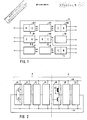
- Fig. 1 is highly schematic and, without making a restriction due to the many variations of integrated circuits, the possible structure of the integrated circuit s is shown, which is realized on a single chip. From the many possible basic circuit types for realizing individual self-contained subfunctions, the analog / digital converter ad, the sample and hold circuit ah, the adder sm, the multiplier m, the memory sp, the digital / analog Converter there, the shift register sr, the gate g and the flip-flops f shown.
- the integrated circuit s can also contain analog stages such as amplifiers etc.
- the external connections on the left side of the integrated circuit s are intended to illustrate input lines and the external connections on the right side are intended to illustrate output lines.
- the subfunctions realized by the basic circuit types mentioned have arrows indicated by output lines which either lead to other subfunctions within the integrated circuit s or also to further output lines.
- the individual subfunctions can also have further input lines which lead to them from other subfunctions of the integrated circuit c.
- the specific design of the linkage of the individual subfunctions depends on the special structure and the overall function of the integrated circuit s for which it is designed. This special internal wiring plays no role in the invention, i.e. the invention is applicable to all integrated circuits.
- the total number p + q of the basic circuit types required for a subfunction is divided according to the invention into the partial numbers p, q so that the operating voltage dependence of the signal delay time of the CMOS basic circuits C is compensated for by the operating voltage dependency of the signal delay time of the NMOS basic circuits N.
- Fig. 2 shows the application of the principle on which the invention is based on a ring oscillator, as is often the case in digital integrated circuits, e.g. is used to generate clock signals or to measure the gate delay.
- a ring oscillator is the phase connection of inverters in phase order for the purpose of vibrating, in which the output of the last is connected to the input of the first, so that they form the "ring".
- an odd number of inverters are generally connected to form a ring.
- one of the inverters e.g. realized as a NOR or NAND gate, via which the "correct" phase condition can be canceled by means of a signal.
- FIG. 2 shows a ring oscillator with seven inverters connected to form a ring.
- the number of parts p is realized by means of the CMOS inverter ic and the number of parts q by means of the depletion load inverter id.
- four CMOS inverters ic and three depletion load inverters id form the ring oscillator, the depletion transistor dl being connected as a corresponding load element.
- the operating voltage independence can be set very precisely by means of the respective layout parameters and the manufacturing parameters.
- the P and N transistors of the CMOS inverters ic each had a channel length of 1.5 micrometers, the P transistor each had a channel width of 30 micrometers and a gate -Threshold voltage of -0.75 V and the N-transistor each one of 15 micrometers or +0.75 V.
- the depletion load inverters in FIG. 2 were divided into two "groups"; in the case of two depletion load inverters, the depletion transistors each had a channel length of 2 micrometers and each had a channel width of 14 micrometers, and the enhancement transistors each had a channel length of 1.5 micrometers and each had a channel width of 15 micrometers.
- the depletion transistor In the third depletion load inverter, the depletion transistor had a channel length of 2 micrometers and a channel width of 20 micrometers, and the enhancement transistor had a channel length of 1.5 micrometers and a channel width of 15 micrometers. All depletion transistors had a gate-source threshold voltage of -2 V and all Enhancement transistors in turn have a gate threshold voltage of +0.75 V.
Priority Applications (4)
| Application Number | Priority Date | Filing Date | Title |
|---|---|---|---|
| EP88105243A EP0334983A1 (fr) | 1988-03-31 | 1988-03-31 | Circuit intégré CMOS/NMOS |
| US07/324,865 US4922140A (en) | 1988-03-31 | 1989-03-17 | CMOS/NMOS integrated circuit with supply voltage delay variation compensation |
| CN89101825.5A CN1036864A (zh) | 1988-03-31 | 1989-03-30 | Cmos/nmos集成电路 |
| JP1081339A JPH0210853A (ja) | 1988-03-31 | 1989-03-31 | Cmos/nmos集積回路 |
Applications Claiming Priority (1)
| Application Number | Priority Date | Filing Date | Title |
|---|---|---|---|
| EP88105243A EP0334983A1 (fr) | 1988-03-31 | 1988-03-31 | Circuit intégré CMOS/NMOS |
Publications (1)
| Publication Number | Publication Date |
|---|---|
| EP0334983A1 true EP0334983A1 (fr) | 1989-10-04 |
Family
ID=8198855
Family Applications (1)
| Application Number | Title | Priority Date | Filing Date |
|---|---|---|---|
| EP88105243A Withdrawn EP0334983A1 (fr) | 1988-03-31 | 1988-03-31 | Circuit intégré CMOS/NMOS |
Country Status (4)
| Country | Link |
|---|---|
| US (1) | US4922140A (fr) |
| EP (1) | EP0334983A1 (fr) |
| JP (1) | JPH0210853A (fr) |
| CN (1) | CN1036864A (fr) |
Cited By (2)
| Publication number | Priority date | Publication date | Assignee | Title |
|---|---|---|---|---|
| EP0429133A2 (fr) * | 1989-11-20 | 1991-05-29 | Philips Patentverwaltung GmbH | Circuit de compensation des variations de largeur d'impulsions |
| EP0704970A1 (fr) * | 1994-09-29 | 1996-04-03 | Valeo Electronique | Circuit monostable à faibles dispersions du temps de basculement et circuit électronique l'incorporant |
Families Citing this family (22)
| Publication number | Priority date | Publication date | Assignee | Title |
|---|---|---|---|---|
| JPH02296410A (ja) * | 1989-05-11 | 1990-12-07 | Mitsubishi Electric Corp | 遅延回路 |
| JPH04172711A (ja) * | 1990-11-06 | 1992-06-19 | Mitsubishi Electric Corp | 半導体遅延回路 |
| US5243227A (en) * | 1991-11-01 | 1993-09-07 | Hewlett-Packard Company | Fine/coarse wired-or tapped delay line |
| US5283631A (en) * | 1991-11-01 | 1994-02-01 | Hewlett-Packard Co. | Programmable capacitance delay element having inverters controlled by adjustable voltage to offset temperature and voltage supply variations |
| US5175512A (en) * | 1992-02-28 | 1992-12-29 | Avasem Corporation | High speed, power supply independent CMOS voltage controlled ring oscillator with level shifting circuit |
| US5254891A (en) * | 1992-04-20 | 1993-10-19 | International Business Machines Corporation | BICMOS ECL circuit suitable for delay regulation |
| WO1994029798A1 (fr) * | 1993-06-08 | 1994-12-22 | National Semiconductor Corporation | Bus cmos programmable et etage d'attaque pour lignes de transmission |
| US5557223A (en) * | 1993-06-08 | 1996-09-17 | National Semiconductor Corporation | CMOS bus and transmission line driver having compensated edge rate control |
| US5483184A (en) * | 1993-06-08 | 1996-01-09 | National Semiconductor Corporation | Programmable CMOS bus and transmission line receiver |
| US5539341A (en) * | 1993-06-08 | 1996-07-23 | National Semiconductor Corporation | CMOS bus and transmission line driver having programmable edge rate control |
| US5543746A (en) * | 1993-06-08 | 1996-08-06 | National Semiconductor Corp. | Programmable CMOS current source having positive temperature coefficient |
| US5818260A (en) * | 1996-04-24 | 1998-10-06 | National Semiconductor Corporation | Transmission line driver having controllable rise and fall times with variable output low and minimal on/off delay |
| US20040263200A1 (en) * | 2003-06-30 | 2004-12-30 | Marijan Persun | A method and apparatus for measuring leakage current and/or temperature variation |
| US7193427B2 (en) * | 2003-06-30 | 2007-03-20 | Intel Corporation | Method and apparatus for measuring relative, within-die leakage current and/or providing a temperature variation profile using a leakage inverter and ring oscillator |
| CN103650345A (zh) | 2011-07-22 | 2014-03-19 | 辉达公司 | 部件分析系统及方法 |
| US9425772B2 (en) | 2011-07-27 | 2016-08-23 | Nvidia Corporation | Coupling resistance and capacitance analysis systems and methods |
| US8952705B2 (en) | 2011-11-01 | 2015-02-10 | Nvidia Corporation | System and method for examining asymetric operations |
| US9448125B2 (en) | 2011-11-01 | 2016-09-20 | Nvidia Corporation | Determining on-chip voltage and temperature |
| EP2757129B1 (fr) * | 2013-01-18 | 2015-07-08 | Akzenta Paneele + Profile GmbH | Panneau de décoration avec plaque de support modifiée par poudre élastomère |
| CN103983809A (zh) | 2013-02-08 | 2014-08-13 | 辉达公司 | Pcb板及其在线测试结构以及该在线测试结构的制造方法 |
| TWI642273B (zh) * | 2017-02-07 | 2018-11-21 | 國立中山大學 | 製程及溫度變異偵測器 |
| US11068237B1 (en) | 2018-07-11 | 2021-07-20 | Rambus Inc. | Dual-domain combinational logic circuitry |
Citations (1)
| Publication number | Priority date | Publication date | Assignee | Title |
|---|---|---|---|---|
| EP0219291A2 (fr) * | 1985-10-07 | 1987-04-22 | Yamaha Corporation | Circuit intégré CMOS destiné à retarder des signaux |
Family Cites Families (9)
| Publication number | Priority date | Publication date | Assignee | Title |
|---|---|---|---|---|
| US3931588A (en) * | 1974-09-10 | 1976-01-06 | Rca Corporation | Voltage controlled oscillator utilizing field effect transistors |
| US4016434A (en) * | 1975-09-04 | 1977-04-05 | International Business Machines Corporation | Load gate compensator circuit |
| US4072910A (en) * | 1976-04-09 | 1978-02-07 | Rca Corporation | Voltage controlled oscillator having equally controlled current source and current sink |
| JPS5772429A (en) * | 1980-10-22 | 1982-05-06 | Toshiba Corp | Semiconductor integrated circuit device |
| US4340867A (en) * | 1980-11-05 | 1982-07-20 | Gte Laboratories Incorporated | Inverter amplifier |
| US4494021A (en) * | 1982-08-30 | 1985-01-15 | Xerox Corporation | Self-calibrated clock and timing signal generator for MOS/VLSI circuitry |
| JPS6025323A (ja) * | 1983-07-22 | 1985-02-08 | Fujitsu Ltd | 半導体集積回路 |
| US4641048A (en) * | 1984-08-24 | 1987-02-03 | Tektronix, Inc. | Digital integrated circuit propagation delay time controller |
| US4737670A (en) * | 1984-11-09 | 1988-04-12 | Lsi Logic Corporation | Delay control circuit |
-
1988
- 1988-03-31 EP EP88105243A patent/EP0334983A1/fr not_active Withdrawn
-
1989
- 1989-03-17 US US07/324,865 patent/US4922140A/en not_active Expired - Fee Related
- 1989-03-30 CN CN89101825.5A patent/CN1036864A/zh active Pending
- 1989-03-31 JP JP1081339A patent/JPH0210853A/ja active Pending
Patent Citations (1)
| Publication number | Priority date | Publication date | Assignee | Title |
|---|---|---|---|---|
| EP0219291A2 (fr) * | 1985-10-07 | 1987-04-22 | Yamaha Corporation | Circuit intégré CMOS destiné à retarder des signaux |
Non-Patent Citations (3)
| Title |
|---|
| IEEE JOURNAL OF SOLID-STATE CIRCUITS * |
| IEEE TRANSACTIONS ON ELECTRON DEVICES * |
| PATENT ABSTRACT OF JAPAN * |
Cited By (4)
| Publication number | Priority date | Publication date | Assignee | Title |
|---|---|---|---|---|
| EP0429133A2 (fr) * | 1989-11-20 | 1991-05-29 | Philips Patentverwaltung GmbH | Circuit de compensation des variations de largeur d'impulsions |
| EP0429133A3 (en) * | 1989-11-20 | 1991-10-30 | Philips Patentverwaltung Gmbh | Circuit for compensating pulse-width variations |
| EP0704970A1 (fr) * | 1994-09-29 | 1996-04-03 | Valeo Electronique | Circuit monostable à faibles dispersions du temps de basculement et circuit électronique l'incorporant |
| FR2725325A1 (fr) * | 1994-09-29 | 1996-04-05 | Valeo Electronique | Circuit monostable a faibles dispersions du temps de basculement et circuit electronique l'incorporant |
Also Published As
| Publication number | Publication date |
|---|---|
| US4922140A (en) | 1990-05-01 |
| CN1036864A (zh) | 1989-11-01 |
| JPH0210853A (ja) | 1990-01-16 |
Similar Documents
| Publication | Publication Date | Title |
|---|---|---|
| EP0334983A1 (fr) | Circuit intégré CMOS/NMOS | |
| EP0059802B1 (fr) | Circuit de ligne à retard intégrée à transistor à effet de champ à couche isolante pour signaux numériques et l'utilisation d'un tel circuit dans les récepteurs de télévision à couleurs | |
| DE2625007C3 (de) | Adressenpufferschaltung für Halbleiterspeicher | |
| DE4238063C2 (de) | Integrierte Speicherzellenschaltung mit Set-/Reset-Funktion | |
| EP0253914A1 (fr) | Etage driver push-pull à transistors à effet de champ à porte isolée comportant une compensation de la fluctuation des paramètres de fonctionnement et de la dispersion de fabrication | |
| DE1942420C3 (de) | Antivalenz/ Äquivalenz-Schaltung mit Feldeffekt-Transistoren | |
| EP1612936A2 (fr) | Dispositif de commande d'horloge | |
| EP0258840A1 (fr) | Registre à approximation successive | |
| EP0352549B1 (fr) | Additionneur à sélection de retenue | |
| DE10062728A1 (de) | Pegelumsetzerschaltung | |
| DE4214981A1 (de) | Asynchrone Logikschaltung für den 2-Phasen-Betrieb | |
| DE3018509A1 (de) | Schieberegister mit latch-schaltung | |
| EP0090904B1 (fr) | Circuit pour filtre numérique opérant en série | |
| DE3314655A1 (de) | Cmos-pufferverstaerker | |
| DE2017132A1 (de) | Binarer Parallel Addierer | |
| DE3834760A1 (de) | Programmierbares logikfeld | |
| DE3144513C1 (de) | Schaltungsanordnung in MOS-Technik zur Erzeugung eines Nachfolgetaktes aus mindestens einem Setztakt | |
| DE2332431A1 (de) | Flip-flop | |
| DE2607045B2 (de) | Elektronische Schaltung mit einem Verstärker | |
| EP0200797A1 (fr) | Circuit intégré monolithique numérique | |
| DE2430349A1 (de) | Verzoegerungsschaltung nach dem prinzip der ladungsverschiebeschaltungen | |
| DE3339985A1 (de) | Schaltungsanordnung zur zaehlung von 1-belegungen in (0,1)-vektoren | |
| DE2834798C3 (de) | Schaltungsanordnung zum Ansteuern einflankengesteuerter Bauelemente | |
| DE2605380B2 (de) | Schaltungsanordnung zum Erzeugen einer Rechteckschwingung aus der Mischung zweier Rechteckschwingungen miteinander | |
| DE2122878C3 (de) | Vier-Phasen-Verzögerungseinheit |
Legal Events
| Date | Code | Title | Description |
|---|---|---|---|
| PUAI | Public reference made under article 153(3) epc to a published international application that has entered the european phase |
Free format text: ORIGINAL CODE: 0009012 |
|
| AK | Designated contracting states |
Kind code of ref document: A1 Designated state(s): DE FR GB IT NL |
|
| 17P | Request for examination filed |
Effective date: 19900403 |
|
| 17Q | First examination report despatched |
Effective date: 19910725 |
|
| STAA | Information on the status of an ep patent application or granted ep patent |
Free format text: STATUS: THE APPLICATION HAS BEEN WITHDRAWN |
|
| 18W | Application withdrawn |
Withdrawal date: 19911128 |