EP0332955A2 - Thyristor ayant une forte capacité de blocage direct et inverse et méthode de fabrication correpondante - Google Patents
Thyristor ayant une forte capacité de blocage direct et inverse et méthode de fabrication correpondante Download PDFInfo
- Publication number
- EP0332955A2 EP0332955A2 EP89103804A EP89103804A EP0332955A2 EP 0332955 A2 EP0332955 A2 EP 0332955A2 EP 89103804 A EP89103804 A EP 89103804A EP 89103804 A EP89103804 A EP 89103804A EP 0332955 A2 EP0332955 A2 EP 0332955A2
- Authority
- EP
- European Patent Office
- Prior art keywords
- semiconductor body
- zone
- type
- base
- semiconductor
- Prior art date
- Legal status (The legal status is an assumption and is not a legal conclusion. Google has not performed a legal analysis and makes no representation as to the accuracy of the status listed.)
- Withdrawn
Links
Images
Classifications
-
- H—ELECTRICITY
- H10—SEMICONDUCTOR DEVICES; ELECTRIC SOLID-STATE DEVICES NOT OTHERWISE PROVIDED FOR
- H10D—INORGANIC ELECTRIC SEMICONDUCTOR DEVICES
- H10D18/00—Thyristors
- H10D18/01—Manufacture or treatment
-
- H—ELECTRICITY
- H10—SEMICONDUCTOR DEVICES; ELECTRIC SOLID-STATE DEVICES NOT OTHERWISE PROVIDED FOR
- H10D—INORGANIC ELECTRIC SEMICONDUCTOR DEVICES
- H10D18/00—Thyristors
-
- H—ELECTRICITY
- H10—SEMICONDUCTOR DEVICES; ELECTRIC SOLID-STATE DEVICES NOT OTHERWISE PROVIDED FOR
- H10D—INORGANIC ELECTRIC SEMICONDUCTOR DEVICES
- H10D62/00—Semiconductor bodies, or regions thereof, of devices having potential barriers
- H10D62/10—Shapes, relative sizes or dispositions of the regions of the semiconductor bodies; Shapes of the semiconductor bodies
- H10D62/102—Constructional design considerations for preventing surface leakage or controlling electric field concentration
- H10D62/103—Constructional design considerations for preventing surface leakage or controlling electric field concentration for increasing or controlling the breakdown voltage of reverse-biased devices
- H10D62/105—Constructional design considerations for preventing surface leakage or controlling electric field concentration for increasing or controlling the breakdown voltage of reverse-biased devices by having particular doping profiles, shapes or arrangements of PN junctions; by having supplementary regions, e.g. junction termination extension [JTE]
-
- Y—GENERAL TAGGING OF NEW TECHNOLOGICAL DEVELOPMENTS; GENERAL TAGGING OF CROSS-SECTIONAL TECHNOLOGIES SPANNING OVER SEVERAL SECTIONS OF THE IPC; TECHNICAL SUBJECTS COVERED BY FORMER USPC CROSS-REFERENCE ART COLLECTIONS [XRACs] AND DIGESTS
- Y10—TECHNICAL SUBJECTS COVERED BY FORMER USPC
- Y10S—TECHNICAL SUBJECTS COVERED BY FORMER USPC CROSS-REFERENCE ART COLLECTIONS [XRACs] AND DIGESTS
- Y10S438/00—Semiconductor device manufacturing: process
- Y10S438/965—Shaped junction formation
Definitions
- the invention relates to a thyristor according to the preamble of claim 1 and to methods for its production.
- a thyristor of this type is known from the "Thyristor Manual” by A. Hoffmann and K. Stocker, Verlag Siemens AG, Berlin and Kunststoff, 1965, pp. 37 and 38, in particular Fig. 8.1.
- a blocking voltage is applied between the anode and cathode of a thyristor, by means of which the anode is placed at a higher potential than the cathode, the pn junction between the n base and the p base is reverse-biased.
- the pn junction between the n base and the p emitter is reverse biased. If the applied blocking voltage exceeds a predetermined limit value, which determines the positive blocking capability (forward blocking capability) of the thyristor, there is a breakdown at the pn junction between the n base and the p base, with the result that the thyristor ignites unintentionally and may be subjected to high thermal loads.
- a predetermined limit value which determines the positive blocking capability (forward blocking capability) of the thyristor
- the applied blocking voltage exceeds a predetermined limit value, which indicates the negative blocking capability of the thyristor, an avalanche breakdown of the pn junction between the n base and the p emitter occurs, which generally thermally overloads the thyristor and thus destroyed.
- the electric field strength is increased at the points where the pn junctions mentioned above reach the semiconductor surface due to the influence of surface charges and edge geometry. As a result, a premature breakthrough occurs at the component edge before the volume locking capability is reached. Therefore, efforts are being made to reduce the surface field strengths that occur at the edges of the pn junctions that are prestressed in the reverse direction.
- the present invention has for its object to provide a thyristor of the type mentioned, which has both a high positive and a high negative blocking ability despite a simple structure. This is achieved according to the invention by training according to the characterizing part of patent claim 1.
- the advantage that can be achieved with the invention is in particular that the edge terminations of the two pn junctions that determine the positive and negative blocking capability are arranged on the upper side of the thyristor semiconductor body and can therefore be designed in a simple manner so that they ensure the desired high blocking capabilities .
- the entire underside of the thyristor semiconductor body is available as a contact surface for a connection to a heat-dissipating substrate wafer, for example made of molybdenum.
- Farther can the edge areas of both blocking pn junctions because of their arrangement on one and the same thyristor side z.
- Claim 2 is directed to a preferred development of the invention.
- Advantageous methods for producing a thyristor according to the invention are specified in claims 3 to 5.
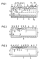
- a semiconductor body 1 shows the cross section of a semiconductor body 1, for example made of n-doped silicon with a doping concentration of approximately 10 13 cm -3, into which a p-type base region 2 is inserted. This is separated from the remaining part of the semiconductor body 1 by a planar pn junction 3.
- the pn junction 3 runs essentially parallel to the upper side 1a of the semiconductor body 1, but gradually approaches the upper side 1a in its edge region and reaches it in a line 4 running perpendicular to the image plane, which represents the lateral boundary of the base region 2.
- a grant material for the base area 2 comes z.
- the doping concentration in the right of the dashed line 5, the central part of 2 is about 101 10cm ⁇ 3 and within the left of 5 part of 2 in the direction of the lateral boundary 4th continuously decreased, so that it finally dropped to a value of about 1013cm ⁇ 3 at 4.
- An n-type emitter region 6 is inserted into the base region 2 and is contacted on the top 1a of the semiconductor body 1 by a cathode-side electrode 7 provided with a cathode connection 8. If further n-type emitter regions are inserted into the base region 2, each of them is contacted by an assigned part of the electrode on the cathode side, these parts being conductively connected to one another and routed to the connection 8.
- the base region 2 is contacted by a gate electrode 9, which is acted upon by a positive ignition voltage pulse supplied via a connection 10 in order to ignite the thyristor.
- the p-emitter of the thyristor consists of a p-type semiconductor layer 11 inserted into the semiconductor body 1 on its underside 1b, on which an anode-side electrode 12 is applied, which is provided with an anode connection 13.
- the part 14 of the semiconductor body 1 located below the base region 2 and above the semiconductor layer forms the n base of the thyristor.
- the p-type semiconductor layer 11 continues in a p-type side zone 15, which is inserted into the semiconductor body 1 at its side edge 16 and extends from the bottom side 1b to the top side 1a thereof. Furthermore, a p-type semiconductor zone 17 is provided in the semiconductor body 1 on the upper side thereof, starting from the part of the side zone 15 lying on the upper side 1 a and along the upper side 1 a in the direction of the lateral boundary 4 of the p-base region 2 extends.
- the semiconductor zone 17 is separated from the part 14 of the semiconductor body 1 by a planar pn junction 18, the pn junction 18 running essentially parallel to the upper side 1a and only being completely in the area of its right edge termination approximates the upper side 1a, which it reaches in the area of a line 20 running perpendicular to the image plane.
- the line 20 represents the lateral boundary of the semiconductor zone 17.
- the doping concentration of the p-type semiconductor layer 11 and the side zone 15 and that of the part of the semiconductor zone 17 to the left of the dashed line 19 is approximately 1018cm83. To the right of line 19, the doping concentration decreases from this value in the direction of the lateral boundary 20 to approximately 10 13 cm 3.
- an n-type semiconductor region 21 is inserted approximately in the middle between the lateral boundaries 4 and 20 of the p-base region 2 or the semiconductor zone 17 in the part 14 of the semiconductor body 1 in such a way that it extends to the top 1a thereof.
- the doping concentration of the semiconductor region 21 can be, for example, 1018cm ⁇ 3.
- a space charge zone is formed at the pn junction 3, which is biased in the blocking direction, the upper and lower limits of which are given by the dashed lines 22 and 23. Because of the above-described course of the pn junction in the region of the edge termination 4, the space charge zone 22 23 is widened on the upper side 1 a, the width of which is indicated on the upper side 1 a by the double arrow 24. This width is so large that the surface field strength occurring at the pn junction 3 under the influence of the blocking voltage is reduced to such an extent that the desired high positive blocking capability is achieved.
- a space charge zone forms at the pn junction 18, which is biased in the reverse direction in this case, and at the pn junctions between the parts 11, 15 and 14, which are also biased in the reverse direction the dashed lines Zungslinien 25 and 26 is indicated.
- the double arrow 27 indicates the expansion of the space charge zone at the top 1a of the semiconductor body 1 achieved by the course of the pn junction 18, which brings about a reduction in the surface field strength occurring in the edge region 20 of the pn junction 18 to values such that the desired high negative blocking ability is achieved.
- an n-conducting semiconductor body 1 is expediently assumed, with a p-type dopant, for example A1, in FIG. 2 in a zone starting from the interfaces of 1, which is indicated by the dashed line 28 the remaining part of FIG. 1 is introduced, namely by means of a first pre-diffusion step, also referred to as "predeposition".
- a corresponding diffusion source is used which, at a predetermined temperature, for example 1060 ° C., introduces the dopant through the interfaces into zone 28 within a predetermined period of time, for example for a period of 7 hours.
- This process can also be understood as a coating of the semiconductor body 1 in the area of its interfaces with the dopant from the gas phase.
- Zone 28 has, for example, a penetration depth of 100 ⁇ m and an edge-side doping concentration in the immediate vicinity of the interfaces of approximately 1019cm ⁇ 3.
- zone 28 is structured in the manner shown in FIG. 2.
- Recesses 29 to 35 are provided in zone 28.
- the top side 1a is first covered with an etching mask, which passes through known photolithographic steps is structured so that it is removed at the locations where the recesses 29 to 35 are provided.
- the recesses 29 to 35 extending up to the line 28 are then produced.
- the bottom surfaces of the recesses 29 to 35 expediently have the shape of concentric circles.
- the size d / w for the recesses 29 to 31 decreases with increasing progress towards the edge closure 4.
- the size d / w for the recesses 32 to 35 also decreases as the edge 20 is approached.
- the recess 32 determines the lateral distance of the edge termination 4 of the p-base region 2 from the edge 20 of the zone 17.
- a tempering step also referred to as post-diffusion, in which the semiconductor body shown in FIG. 2 while removing the diffusion mask for a predetermined period of time, e.g. Exposed to a temperature of about 1240 ° C for 20 hours.
- the dopant atoms introduced into zone 28 diffuse further into the semiconductor body 1 from the parts of zone 28 remaining according to FIG. 2, so that finally the pn junctions 3, 18, 36 and 37 appear.
- the semiconductor parts 2, 11, 15 and 17 are produced according to FIG. 1.
- the inner part of the p-base region 2 is formed under the part of the upper side 1a of the semiconductor body 1 which is laterally encompassed by the recesses 29 to 35.
- the n-type regions 6 and 21 are inserted. Regions 6, 2 and 11 are then contacted with electrodes 7, 9 and 12.
- the production method described with reference to FIG. 2 largely corresponds to the method for producing a pn junction, which is specified in EP-A 0 262 356.
- Fig. 3 illustrates another method for producing a thyristor according to the invention.
- the upper side 1a of the semiconductor body 1 is provided with a doping mask M, in which openings 38 to 45 are provided.
- the openings 38 to 41 are dimensioned smaller with increasing approach to the line 4.
- the openings 42 to 44 are sized smaller as the line 20 approaches.
- opening 38 defines the inner part of p-base region 2, while further, substantially smaller openings 39 to 41 define the edge region of FIG. 2.
- the edge-side opening 45 defines the essential part of the p-type semiconductor zone 17, while the substantially smaller openings 42 to 44 define the edge region of FIG. 17.
- the dopant required for the formation of regions 2, 11, 15 and 17 is introduced into the semiconductor body 1 by means of a diffusion step in such a way that the pn junctions 3 and 18, as well as those between parts 11, 15 and 14, result directly.
- the regions 6 and 21 are inserted in the manner already described and the regions 6, 2 and 11 are provided with the electrodes 7, 9 and 12.
- a production process of this type has already been described in EP-A 0 176 778.
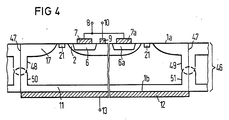
- a wafer-like, n-type semiconductor body 46 which is shown in FIG. 4 and is intended for a plurality of such thyristors, is assumed, then at the interfaces 47 separating the individual thyristors from one another, p- Separation diffusions added.
- This is understood to mean the masked diffusion of a p-type dopant, through which p-diffusion regions 48 and 49 are inserted from the top side 1a and 50 and 51 from the bottom side 1b of the semiconductor body.
- the depths of penetration of regions 48 and 50 are chosen so large that a continuous p-type diffusion region 48, 50 results.
- Regions 49 and 51 likewise form a continuous diffusion region 49, 51.
- the parts of the p-diffusion regions 48 and 50 or 49 and 51 which are approximately halved by the separation lie on the separating surfaces 47 in the embodiment of a thyristor according to the invention shown in FIG. 4, the lateral zones 15 of the same.
- corresponding implantation steps can also be carried out in the production method according to the invention in order to define the p-type regions defined in the semiconductor body 1.
- Corresponding deep implantations or high-energy implantations can in particular take the place of the separation diffusion regions 48 to 51.
Landscapes
- Thyristors (AREA)
Applications Claiming Priority (2)
| Application Number | Priority Date | Filing Date | Title |
|---|---|---|---|
| DE3808666 | 1988-03-15 | ||
| DE3808666 | 1988-03-15 |
Publications (2)
| Publication Number | Publication Date |
|---|---|
| EP0332955A2 true EP0332955A2 (fr) | 1989-09-20 |
| EP0332955A3 EP0332955A3 (fr) | 1991-08-21 |
Family
ID=6349807
Family Applications (1)
| Application Number | Title | Priority Date | Filing Date |
|---|---|---|---|
| EP19890103804 Withdrawn EP0332955A3 (fr) | 1988-03-15 | 1989-03-03 | Thyristor ayant une forte capacité de blocage direct et inverse et méthode de fabrication correpondante |
Country Status (3)
| Country | Link |
|---|---|
| US (2) | US5072312A (fr) |
| EP (1) | EP0332955A3 (fr) |
| JP (1) | JPH01274471A (fr) |
Cited By (1)
| Publication number | Priority date | Publication date | Assignee | Title |
|---|---|---|---|---|
| WO1991017570A1 (fr) * | 1990-04-27 | 1991-11-14 | Lucas Industries Public Limited Company | Transistor bipolaire a grille isolee |
Families Citing this family (13)
| Publication number | Priority date | Publication date | Assignee | Title |
|---|---|---|---|---|
| US5240865A (en) * | 1990-07-30 | 1993-08-31 | Texas Instruments Incorporated | Method of forming a thyristor on an SOI substrate |
| US5204273A (en) * | 1990-08-20 | 1993-04-20 | Siemens Aktiengesellschaft | Method for the manufacturing of a thyristor with defined lateral resistor |
| FR2666174B1 (fr) * | 1990-08-21 | 1997-03-21 | Sgs Thomson Microelectronics | Composant semiconducteur haute tension a faible courant de fuite. |
| JP3387267B2 (ja) * | 1994-10-26 | 2003-03-17 | 味の素株式会社 | トランスグルタミナーゼを用いるチーズの製造方法 |
| US5698454A (en) * | 1995-07-31 | 1997-12-16 | Ixys Corporation | Method of making a reverse blocking IGBT |
| US6727527B1 (en) | 1995-07-31 | 2004-04-27 | Ixys Corporation | Reverse blocking IGBT |
| US20040061170A1 (en) * | 1995-07-31 | 2004-04-01 | Ixys Corporation | Reverse blocking IGBT |
| FR2751790B1 (fr) * | 1996-07-26 | 1998-11-27 | Sgs Thomson Microelectronics | Assemblage monolithique d'un transistor igbt et d'une diode rapide |
| DE59913288D1 (de) | 1998-02-03 | 2006-05-18 | Infineon Technologies Ag | Verfahren zur Herstellung eines beidseitig sperrenden Leistungshalbleiters |
| US6936908B2 (en) * | 2001-05-03 | 2005-08-30 | Ixys Corporation | Forward and reverse blocking devices |
| US7462553B2 (en) * | 2003-06-25 | 2008-12-09 | Semicoa | Ultra thin back-illuminated photodiode array fabrication methods |
| US6762473B1 (en) * | 2003-06-25 | 2004-07-13 | Semicoa Semiconductors | Ultra thin back-illuminated photodiode array structures and fabrication methods |
| US7576371B1 (en) | 2006-03-03 | 2009-08-18 | Array Optronix, Inc. | Structures and methods to improve the crosstalk between adjacent pixels of back-illuminated photodiode arrays |
Family Cites Families (23)
| Publication number | Priority date | Publication date | Assignee | Title |
|---|---|---|---|---|
| FR1529195A (fr) * | 1966-06-28 | 1968-06-14 | Asea Ab | Dispositif à semi-conducteur |
| CH517378A (de) * | 1971-01-12 | 1971-12-31 | Transistor Ag | Halbleiteranordnung mit mindestens einem planaren pn-Uebergang |
| JPS53145483A (en) * | 1977-05-25 | 1978-12-18 | Hitachi Ltd | Semiconductor device and production of the same |
| JPS5419374A (en) * | 1977-07-14 | 1979-02-14 | Mitsubishi Electric Corp | Semiconductor device |
| US4569118A (en) * | 1977-12-23 | 1986-02-11 | General Electric Company | Planar gate turn-off field controlled thyristors and planar junction gate field effect transistors, and method of making same |
| JPS57196570A (en) * | 1981-05-28 | 1982-12-02 | Toshiba Corp | Thyristor |
| US4587712A (en) * | 1981-11-23 | 1986-05-13 | General Electric Company | Method for making vertical channel field controlled device employing a recessed gate structure |
| US4555845A (en) * | 1982-10-13 | 1985-12-03 | Westinghouse Electric Corp. | Temperature stable self-protected thyristor and method of producing |
| JPS5979571A (ja) * | 1982-10-29 | 1984-05-08 | Toshiba Corp | サイリスタ |
| US4516315A (en) * | 1983-05-09 | 1985-05-14 | Westinghouse Electric Corp. | Method of making a self-protected thyristor |
| JPH0691244B2 (ja) * | 1984-04-27 | 1994-11-14 | 三菱電機株式会社 | ゲートターンオフサイリスタの製造方法 |
| EP0176778B1 (fr) * | 1984-09-28 | 1991-01-16 | Siemens Aktiengesellschaft | Procédé pour fabriquer une jonction pn à haute tension de etaquage |
| JPS61105849A (ja) * | 1984-10-30 | 1986-05-23 | Internatl Rectifier Corp Japan Ltd | 半導体装置の製造方法 |
| JPS61114574A (ja) * | 1984-11-09 | 1986-06-02 | Hitachi Ltd | 半導体装置 |
| JPS62199062A (ja) * | 1986-02-27 | 1987-09-02 | Toshiba Corp | 半導体装置 |
| JPS62289544A (ja) * | 1986-06-09 | 1987-12-16 | Daikin Ind Ltd | 含フツ素化合物 |
| JPS639974A (ja) * | 1986-06-30 | 1988-01-16 | Nec Corp | プレ−ナ型半導体装置 |
| JPS6354768A (ja) * | 1986-08-25 | 1988-03-09 | Nec Corp | プレ−ナ型サイリスタ |
| EP0262356B1 (fr) * | 1986-09-30 | 1993-03-31 | Siemens Aktiengesellschaft | Méthode de fabrication d'une jonction P-N à haute tenue en tension |
| US4792530A (en) * | 1987-03-30 | 1988-12-20 | International Rectifier Corporation | Process for balancing forward and reverse characteristic of thyristors |
| EP0310836A3 (fr) * | 1987-10-08 | 1989-06-14 | Siemens Aktiengesellschaft | Elément semi-conducteur avec une jonction pn planaire |
| US4861731A (en) * | 1988-02-02 | 1989-08-29 | General Motors Corporation | Method of fabricating a lateral dual gate thyristor |
| FR2640082B1 (fr) * | 1988-12-07 | 1991-03-29 | Telemecanique | Dispositif semiconducteur de puissance symetrique et son procede de fabrication |
-
1989
- 1989-02-16 US US07/310,960 patent/US5072312A/en not_active Expired - Fee Related
- 1989-03-03 EP EP19890103804 patent/EP0332955A3/fr not_active Withdrawn
- 1989-03-13 JP JP1061982A patent/JPH01274471A/ja active Pending
-
1991
- 1991-06-27 US US07/722,176 patent/US5077224A/en not_active Expired - Fee Related
Cited By (1)
| Publication number | Priority date | Publication date | Assignee | Title |
|---|---|---|---|---|
| WO1991017570A1 (fr) * | 1990-04-27 | 1991-11-14 | Lucas Industries Public Limited Company | Transistor bipolaire a grille isolee |
Also Published As
| Publication number | Publication date |
|---|---|
| US5077224A (en) | 1991-12-31 |
| EP0332955A3 (fr) | 1991-08-21 |
| US5072312A (en) | 1991-12-10 |
| JPH01274471A (ja) | 1989-11-02 |
Similar Documents
| Publication | Publication Date | Title |
|---|---|---|
| EP0360036B1 (fr) | Jonction pn plane à tenue en tension élévée | |
| DE68926261T2 (de) | Symmetrische sperrende Hochdurchbruchspannungshalbleiteranordnung und Verfahren zur Herstellung | |
| DE69331512T2 (de) | Bipolarer Transistor mit isolierter Steuerelektrode und Verfahren zur Herstellung desselben | |
| DE3131727C2 (fr) | ||
| AT404525B (de) | Leistungstransistorvorrichtung und verfahren zu deren herstellung | |
| DE19704996C2 (de) | Verfahren zur Herstellung eines IGBT-Bauelementes | |
| DE112019003790T5 (de) | Superjunction-siliziumkarbid-halbleitervorrichtung und verfahren zum herstellen einer superjunction-siliziumkarbid-halbleitervorrichtung | |
| EP0343369A1 (fr) | Méthode de fabrication d'un thyristor | |
| CH642485A5 (de) | Leistungs-mosfet-anordnung. | |
| DE3505393A1 (de) | Vertikaler feldeffekttransistor und verfahren zum herstellen eines solchen bauelements | |
| DE102009038731A1 (de) | Halbleiterbauelement mit Ladungsträgerkompensationsstruktur und Verfahren zur Herstellung eines Halbleiterbauelements | |
| DE19701189A1 (de) | Halbleiterbauteil | |
| DE19813509A1 (de) | Thyristor mit isoliertem Gate | |
| CH668505A5 (de) | Halbleiterbauelement. | |
| DE102007057728A1 (de) | Halbleiterbauelement mit einer Kurzschlussstruktur, die einen Teiltransistor des Halbleiterbauelements umfasst, der eine geringe Temperaturabhängigkeit aufweist und Verfahren zur Herstellung eines solchen Halbleiterbauelements | |
| DE10047152B4 (de) | Hochvolt-Diode und Verfahren zu deren Herstellung | |
| EP0332955A2 (fr) | Thyristor ayant une forte capacité de blocage direct et inverse et méthode de fabrication correpondante | |
| EP1131852B1 (fr) | Composant semi-conducteur dote de structures de blindage dielectriques ou semi-isolantes | |
| DE10240107B4 (de) | Randabschluss für Leistungshalbleiterbauelement und für Diode sowie Verfahren zur Herstellung einer n-leitenden Zone für einen solchen Randabschluss | |
| DE102021103703A1 (de) | Hochvolt-Randabschluss-Struktur für Leistungshalbleiterbauelemente und Verfahren zum Herstellen derselben | |
| DE1207502B (de) | Flaechenhaftes Halbleiterbauelement mit mindestens einem sperrenden pn-UEbergang und Verfahren zum Herstellen | |
| DE2633324C2 (de) | Verfahren zum Herstellen von Halbleiterbauelementen hoher Sperrspannungsbelastbarkeit | |
| EP0710988A2 (fr) | Procédé pour la fabrication des dispositifs semiconducteurs controlables par effet de champ | |
| EP0017980B1 (fr) | Thyristor contrôlé par un transistor à effet de champ | |
| DE102005038260B3 (de) | Halbleiterbauteil sowie Verfahren zu dessen Herstellung |
Legal Events
| Date | Code | Title | Description |
|---|---|---|---|
| PUAI | Public reference made under article 153(3) epc to a published international application that has entered the european phase |
Free format text: ORIGINAL CODE: 0009012 |
|
| AK | Designated contracting states |
Kind code of ref document: A2 Designated state(s): CH DE FR GB LI SE |
|
| 17P | Request for examination filed |
Effective date: 19901205 |
|
| PUAL | Search report despatched |
Free format text: ORIGINAL CODE: 0009013 |
|
| AK | Designated contracting states |
Kind code of ref document: A3 Designated state(s): CH DE FR GB LI SE |
|
| 17Q | First examination report despatched |
Effective date: 19931021 |
|
| STAA | Information on the status of an ep patent application or granted ep patent |
Free format text: STATUS: THE APPLICATION IS DEEMED TO BE WITHDRAWN |
|
| 18D | Application deemed to be withdrawn |
Effective date: 19940301 |