EP0332955A2 - Thyristor having a large forward and reverse blocking capability, and method of making the same - Google Patents
Thyristor having a large forward and reverse blocking capability, and method of making the same Download PDFInfo
- Publication number
- EP0332955A2 EP0332955A2 EP89103804A EP89103804A EP0332955A2 EP 0332955 A2 EP0332955 A2 EP 0332955A2 EP 89103804 A EP89103804 A EP 89103804A EP 89103804 A EP89103804 A EP 89103804A EP 0332955 A2 EP0332955 A2 EP 0332955A2
- Authority
- EP
- European Patent Office
- Prior art keywords
- semiconductor body
- zone
- type
- semiconductor
- base
- Prior art date
- Legal status (The legal status is an assumption and is not a legal conclusion. Google has not performed a legal analysis and makes no representation as to the accuracy of the status listed.)
- Withdrawn
Links
- 230000000903 blocking effect Effects 0.000 title claims description 18
- 238000004519 manufacturing process Methods 0.000 title claims description 14
- 239000004065 semiconductor Substances 0.000 claims abstract description 77
- 238000013459 approach Methods 0.000 claims abstract description 8
- 238000009792 diffusion process Methods 0.000 claims description 19
- 239000002019 doping agent Substances 0.000 claims description 11
- 238000000034 method Methods 0.000 claims description 10
- 238000002513 implantation Methods 0.000 claims description 6
- 238000005530 etching Methods 0.000 claims description 3
- 238000005496 tempering Methods 0.000 claims description 2
- 239000007943 implant Substances 0.000 claims 1
- 230000002093 peripheral effect Effects 0.000 abstract 2
- 230000015556 catabolic process Effects 0.000 description 3
- 230000007423 decrease Effects 0.000 description 3
- 238000000926 separation method Methods 0.000 description 3
- 230000035515 penetration Effects 0.000 description 2
- IUVCFHHAEHNCFT-INIZCTEOSA-N 2-[(1s)-1-[4-amino-3-(3-fluoro-4-propan-2-yloxyphenyl)pyrazolo[3,4-d]pyrimidin-1-yl]ethyl]-6-fluoro-3-(3-fluorophenyl)chromen-4-one Chemical compound C1=C(F)C(OC(C)C)=CC=C1C(C1=C(N)N=CN=C11)=NN1[C@@H](C)C1=C(C=2C=C(F)C=CC=2)C(=O)C2=CC(F)=CC=C2O1 IUVCFHHAEHNCFT-INIZCTEOSA-N 0.000 description 1
- ZOKXTWBITQBERF-UHFFFAOYSA-N Molybdenum Chemical compound [Mo] ZOKXTWBITQBERF-UHFFFAOYSA-N 0.000 description 1
- 229910021417 amorphous silicon Inorganic materials 0.000 description 1
- 230000015572 biosynthetic process Effects 0.000 description 1
- 239000003795 chemical substances by application Substances 0.000 description 1
- 239000011248 coating agent Substances 0.000 description 1
- 238000000576 coating method Methods 0.000 description 1
- 230000003247 decreasing effect Effects 0.000 description 1
- 238000013461 design Methods 0.000 description 1
- 238000011161 development Methods 0.000 description 1
- 230000005684 electric field Effects 0.000 description 1
- 239000011521 glass Substances 0.000 description 1
- 239000000463 material Substances 0.000 description 1
- 229910052750 molybdenum Inorganic materials 0.000 description 1
- 239000011733 molybdenum Substances 0.000 description 1
- 238000002161 passivation Methods 0.000 description 1
- 229910021420 polycrystalline silicon Inorganic materials 0.000 description 1
- 229920005591 polysilicon Polymers 0.000 description 1
- 230000002028 premature Effects 0.000 description 1
- 229910052710 silicon Inorganic materials 0.000 description 1
- 239000010703 silicon Substances 0.000 description 1
- 239000000758 substrate Substances 0.000 description 1
- 238000012549 training Methods 0.000 description 1
Images
Classifications
-
- H—ELECTRICITY
- H01—ELECTRIC ELEMENTS
- H01L—SEMICONDUCTOR DEVICES NOT COVERED BY CLASS H10
- H01L29/00—Semiconductor devices adapted for rectifying, amplifying, oscillating or switching, or capacitors or resistors with at least one potential-jump barrier or surface barrier, e.g. PN junction depletion layer or carrier concentration layer; Details of semiconductor bodies or of electrodes thereof ; Multistep manufacturing processes therefor
- H01L29/66—Types of semiconductor device ; Multistep manufacturing processes therefor
- H01L29/66007—Multistep manufacturing processes
- H01L29/66075—Multistep manufacturing processes of devices having semiconductor bodies comprising group 14 or group 13/15 materials
- H01L29/66227—Multistep manufacturing processes of devices having semiconductor bodies comprising group 14 or group 13/15 materials the devices being controllable only by the electric current supplied or the electric potential applied, to an electrode which does not carry the current to be rectified, amplified or switched, e.g. three-terminal devices
- H01L29/66363—Thyristors
-
- H—ELECTRICITY
- H01—ELECTRIC ELEMENTS
- H01L—SEMICONDUCTOR DEVICES NOT COVERED BY CLASS H10
- H01L29/00—Semiconductor devices adapted for rectifying, amplifying, oscillating or switching, or capacitors or resistors with at least one potential-jump barrier or surface barrier, e.g. PN junction depletion layer or carrier concentration layer; Details of semiconductor bodies or of electrodes thereof ; Multistep manufacturing processes therefor
- H01L29/02—Semiconductor bodies ; Multistep manufacturing processes therefor
- H01L29/06—Semiconductor bodies ; Multistep manufacturing processes therefor characterised by their shape; characterised by the shapes, relative sizes, or dispositions of the semiconductor regions ; characterised by the concentration or distribution of impurities within semiconductor regions
- H01L29/0603—Semiconductor bodies ; Multistep manufacturing processes therefor characterised by their shape; characterised by the shapes, relative sizes, or dispositions of the semiconductor regions ; characterised by the concentration or distribution of impurities within semiconductor regions characterised by particular constructional design considerations, e.g. for preventing surface leakage, for controlling electric field concentration or for internal isolations regions
- H01L29/0607—Semiconductor bodies ; Multistep manufacturing processes therefor characterised by their shape; characterised by the shapes, relative sizes, or dispositions of the semiconductor regions ; characterised by the concentration or distribution of impurities within semiconductor regions characterised by particular constructional design considerations, e.g. for preventing surface leakage, for controlling electric field concentration or for internal isolations regions for preventing surface leakage or controlling electric field concentration
- H01L29/0611—Semiconductor bodies ; Multistep manufacturing processes therefor characterised by their shape; characterised by the shapes, relative sizes, or dispositions of the semiconductor regions ; characterised by the concentration or distribution of impurities within semiconductor regions characterised by particular constructional design considerations, e.g. for preventing surface leakage, for controlling electric field concentration or for internal isolations regions for preventing surface leakage or controlling electric field concentration for increasing or controlling the breakdown voltage of reverse biased devices
- H01L29/0615—Semiconductor bodies ; Multistep manufacturing processes therefor characterised by their shape; characterised by the shapes, relative sizes, or dispositions of the semiconductor regions ; characterised by the concentration or distribution of impurities within semiconductor regions characterised by particular constructional design considerations, e.g. for preventing surface leakage, for controlling electric field concentration or for internal isolations regions for preventing surface leakage or controlling electric field concentration for increasing or controlling the breakdown voltage of reverse biased devices by the doping profile or the shape or the arrangement of the PN junction, or with supplementary regions, e.g. junction termination extension [JTE]
-
- H—ELECTRICITY
- H01—ELECTRIC ELEMENTS
- H01L—SEMICONDUCTOR DEVICES NOT COVERED BY CLASS H10
- H01L29/00—Semiconductor devices adapted for rectifying, amplifying, oscillating or switching, or capacitors or resistors with at least one potential-jump barrier or surface barrier, e.g. PN junction depletion layer or carrier concentration layer; Details of semiconductor bodies or of electrodes thereof ; Multistep manufacturing processes therefor
- H01L29/66—Types of semiconductor device ; Multistep manufacturing processes therefor
- H01L29/68—Types of semiconductor device ; Multistep manufacturing processes therefor controllable by only the electric current supplied, or only the electric potential applied, to an electrode which does not carry the current to be rectified, amplified or switched
- H01L29/70—Bipolar devices
- H01L29/74—Thyristor-type devices, e.g. having four-zone regenerative action
-
- Y—GENERAL TAGGING OF NEW TECHNOLOGICAL DEVELOPMENTS; GENERAL TAGGING OF CROSS-SECTIONAL TECHNOLOGIES SPANNING OVER SEVERAL SECTIONS OF THE IPC; TECHNICAL SUBJECTS COVERED BY FORMER USPC CROSS-REFERENCE ART COLLECTIONS [XRACs] AND DIGESTS
- Y10—TECHNICAL SUBJECTS COVERED BY FORMER USPC
- Y10S—TECHNICAL SUBJECTS COVERED BY FORMER USPC CROSS-REFERENCE ART COLLECTIONS [XRACs] AND DIGESTS
- Y10S438/00—Semiconductor device manufacturing: process
- Y10S438/965—Shaped junction formation
Definitions
- the invention relates to a thyristor according to the preamble of claim 1 and to methods for its production.
- a thyristor of this type is known from the "Thyristor Manual” by A. Hoffmann and K. Stocker, Verlag Siemens AG, Berlin and Kunststoff, 1965, pp. 37 and 38, in particular Fig. 8.1.
- a blocking voltage is applied between the anode and cathode of a thyristor, by means of which the anode is placed at a higher potential than the cathode, the pn junction between the n base and the p base is reverse-biased.
- the pn junction between the n base and the p emitter is reverse biased. If the applied blocking voltage exceeds a predetermined limit value, which determines the positive blocking capability (forward blocking capability) of the thyristor, there is a breakdown at the pn junction between the n base and the p base, with the result that the thyristor ignites unintentionally and may be subjected to high thermal loads.
- a predetermined limit value which determines the positive blocking capability (forward blocking capability) of the thyristor
- the applied blocking voltage exceeds a predetermined limit value, which indicates the negative blocking capability of the thyristor, an avalanche breakdown of the pn junction between the n base and the p emitter occurs, which generally thermally overloads the thyristor and thus destroyed.
- the electric field strength is increased at the points where the pn junctions mentioned above reach the semiconductor surface due to the influence of surface charges and edge geometry. As a result, a premature breakthrough occurs at the component edge before the volume locking capability is reached. Therefore, efforts are being made to reduce the surface field strengths that occur at the edges of the pn junctions that are prestressed in the reverse direction.
- the present invention has for its object to provide a thyristor of the type mentioned, which has both a high positive and a high negative blocking ability despite a simple structure. This is achieved according to the invention by training according to the characterizing part of patent claim 1.
- the advantage that can be achieved with the invention is in particular that the edge terminations of the two pn junctions that determine the positive and negative blocking capability are arranged on the upper side of the thyristor semiconductor body and can therefore be designed in a simple manner so that they ensure the desired high blocking capabilities .
- the entire underside of the thyristor semiconductor body is available as a contact surface for a connection to a heat-dissipating substrate wafer, for example made of molybdenum.
- Farther can the edge areas of both blocking pn junctions because of their arrangement on one and the same thyristor side z.
- Claim 2 is directed to a preferred development of the invention.
- Advantageous methods for producing a thyristor according to the invention are specified in claims 3 to 5.
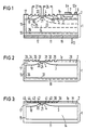
- a semiconductor body 1 shows the cross section of a semiconductor body 1, for example made of n-doped silicon with a doping concentration of approximately 10 13 cm -3, into which a p-type base region 2 is inserted. This is separated from the remaining part of the semiconductor body 1 by a planar pn junction 3.
- the pn junction 3 runs essentially parallel to the upper side 1a of the semiconductor body 1, but gradually approaches the upper side 1a in its edge region and reaches it in a line 4 running perpendicular to the image plane, which represents the lateral boundary of the base region 2.
- a grant material for the base area 2 comes z.
- the doping concentration in the right of the dashed line 5, the central part of 2 is about 101 10cm ⁇ 3 and within the left of 5 part of 2 in the direction of the lateral boundary 4th continuously decreased, so that it finally dropped to a value of about 1013cm ⁇ 3 at 4.
- An n-type emitter region 6 is inserted into the base region 2 and is contacted on the top 1a of the semiconductor body 1 by a cathode-side electrode 7 provided with a cathode connection 8. If further n-type emitter regions are inserted into the base region 2, each of them is contacted by an assigned part of the electrode on the cathode side, these parts being conductively connected to one another and routed to the connection 8.
- the base region 2 is contacted by a gate electrode 9, which is acted upon by a positive ignition voltage pulse supplied via a connection 10 in order to ignite the thyristor.
- the p-emitter of the thyristor consists of a p-type semiconductor layer 11 inserted into the semiconductor body 1 on its underside 1b, on which an anode-side electrode 12 is applied, which is provided with an anode connection 13.
- the part 14 of the semiconductor body 1 located below the base region 2 and above the semiconductor layer forms the n base of the thyristor.
- the p-type semiconductor layer 11 continues in a p-type side zone 15, which is inserted into the semiconductor body 1 at its side edge 16 and extends from the bottom side 1b to the top side 1a thereof. Furthermore, a p-type semiconductor zone 17 is provided in the semiconductor body 1 on the upper side thereof, starting from the part of the side zone 15 lying on the upper side 1 a and along the upper side 1 a in the direction of the lateral boundary 4 of the p-base region 2 extends.
- the semiconductor zone 17 is separated from the part 14 of the semiconductor body 1 by a planar pn junction 18, the pn junction 18 running essentially parallel to the upper side 1a and only being completely in the area of its right edge termination approximates the upper side 1a, which it reaches in the area of a line 20 running perpendicular to the image plane.
- the line 20 represents the lateral boundary of the semiconductor zone 17.
- the doping concentration of the p-type semiconductor layer 11 and the side zone 15 and that of the part of the semiconductor zone 17 to the left of the dashed line 19 is approximately 1018cm83. To the right of line 19, the doping concentration decreases from this value in the direction of the lateral boundary 20 to approximately 10 13 cm 3.
- an n-type semiconductor region 21 is inserted approximately in the middle between the lateral boundaries 4 and 20 of the p-base region 2 or the semiconductor zone 17 in the part 14 of the semiconductor body 1 in such a way that it extends to the top 1a thereof.
- the doping concentration of the semiconductor region 21 can be, for example, 1018cm ⁇ 3.
- a space charge zone is formed at the pn junction 3, which is biased in the blocking direction, the upper and lower limits of which are given by the dashed lines 22 and 23. Because of the above-described course of the pn junction in the region of the edge termination 4, the space charge zone 22 23 is widened on the upper side 1 a, the width of which is indicated on the upper side 1 a by the double arrow 24. This width is so large that the surface field strength occurring at the pn junction 3 under the influence of the blocking voltage is reduced to such an extent that the desired high positive blocking capability is achieved.
- a space charge zone forms at the pn junction 18, which is biased in the reverse direction in this case, and at the pn junctions between the parts 11, 15 and 14, which are also biased in the reverse direction the dashed lines Zungslinien 25 and 26 is indicated.
- the double arrow 27 indicates the expansion of the space charge zone at the top 1a of the semiconductor body 1 achieved by the course of the pn junction 18, which brings about a reduction in the surface field strength occurring in the edge region 20 of the pn junction 18 to values such that the desired high negative blocking ability is achieved.
- an n-conducting semiconductor body 1 is expediently assumed, with a p-type dopant, for example A1, in FIG. 2 in a zone starting from the interfaces of 1, which is indicated by the dashed line 28 the remaining part of FIG. 1 is introduced, namely by means of a first pre-diffusion step, also referred to as "predeposition".
- a corresponding diffusion source is used which, at a predetermined temperature, for example 1060 ° C., introduces the dopant through the interfaces into zone 28 within a predetermined period of time, for example for a period of 7 hours.
- This process can also be understood as a coating of the semiconductor body 1 in the area of its interfaces with the dopant from the gas phase.
- Zone 28 has, for example, a penetration depth of 100 ⁇ m and an edge-side doping concentration in the immediate vicinity of the interfaces of approximately 1019cm ⁇ 3.
- zone 28 is structured in the manner shown in FIG. 2.
- Recesses 29 to 35 are provided in zone 28.
- the top side 1a is first covered with an etching mask, which passes through known photolithographic steps is structured so that it is removed at the locations where the recesses 29 to 35 are provided.
- the recesses 29 to 35 extending up to the line 28 are then produced.
- the bottom surfaces of the recesses 29 to 35 expediently have the shape of concentric circles.
- the size d / w for the recesses 29 to 31 decreases with increasing progress towards the edge closure 4.
- the size d / w for the recesses 32 to 35 also decreases as the edge 20 is approached.
- the recess 32 determines the lateral distance of the edge termination 4 of the p-base region 2 from the edge 20 of the zone 17.
- a tempering step also referred to as post-diffusion, in which the semiconductor body shown in FIG. 2 while removing the diffusion mask for a predetermined period of time, e.g. Exposed to a temperature of about 1240 ° C for 20 hours.
- the dopant atoms introduced into zone 28 diffuse further into the semiconductor body 1 from the parts of zone 28 remaining according to FIG. 2, so that finally the pn junctions 3, 18, 36 and 37 appear.
- the semiconductor parts 2, 11, 15 and 17 are produced according to FIG. 1.
- the inner part of the p-base region 2 is formed under the part of the upper side 1a of the semiconductor body 1 which is laterally encompassed by the recesses 29 to 35.
- the n-type regions 6 and 21 are inserted. Regions 6, 2 and 11 are then contacted with electrodes 7, 9 and 12.
- the production method described with reference to FIG. 2 largely corresponds to the method for producing a pn junction, which is specified in EP-A 0 262 356.
- Fig. 3 illustrates another method for producing a thyristor according to the invention.
- the upper side 1a of the semiconductor body 1 is provided with a doping mask M, in which openings 38 to 45 are provided.
- the openings 38 to 41 are dimensioned smaller with increasing approach to the line 4.
- the openings 42 to 44 are sized smaller as the line 20 approaches.
- opening 38 defines the inner part of p-base region 2, while further, substantially smaller openings 39 to 41 define the edge region of FIG. 2.
- the edge-side opening 45 defines the essential part of the p-type semiconductor zone 17, while the substantially smaller openings 42 to 44 define the edge region of FIG. 17.
- the dopant required for the formation of regions 2, 11, 15 and 17 is introduced into the semiconductor body 1 by means of a diffusion step in such a way that the pn junctions 3 and 18, as well as those between parts 11, 15 and 14, result directly.
- the regions 6 and 21 are inserted in the manner already described and the regions 6, 2 and 11 are provided with the electrodes 7, 9 and 12.
- a production process of this type has already been described in EP-A 0 176 778.
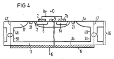
- a wafer-like, n-type semiconductor body 46 which is shown in FIG. 4 and is intended for a plurality of such thyristors, is assumed, then at the interfaces 47 separating the individual thyristors from one another, p- Separation diffusions added.
- This is understood to mean the masked diffusion of a p-type dopant, through which p-diffusion regions 48 and 49 are inserted from the top side 1a and 50 and 51 from the bottom side 1b of the semiconductor body.
- the depths of penetration of regions 48 and 50 are chosen so large that a continuous p-type diffusion region 48, 50 results.
- Regions 49 and 51 likewise form a continuous diffusion region 49, 51.
- the parts of the p-diffusion regions 48 and 50 or 49 and 51 which are approximately halved by the separation lie on the separating surfaces 47 in the embodiment of a thyristor according to the invention shown in FIG. 4, the lateral zones 15 of the same.
- corresponding implantation steps can also be carried out in the production method according to the invention in order to define the p-type regions defined in the semiconductor body 1.
- Corresponding deep implantations or high-energy implantations can in particular take the place of the separation diffusion regions 48 to 51.
Abstract
Description
Die Erfindung bezieht sich auf einen Thyristor nach dem Oberbegriff des Patentanspruchs 1 sowie auf Verfahren zu dessen Herstellung.The invention relates to a thyristor according to the preamble of claim 1 and to methods for its production.
Ein Thyristor dieser Art ist aus dem "Thyristor-Handbuch" von A. Hoffmann und K. Stocker, Verlag Siemens AG, Berlin und München, 1965, S. 37 und 38, insbesondere Bild 8.1, bekannt. Wie in dem Buch von P. D. Taylor "ThyristorDdesign and Realization", Verlag John Wiley and Sons, New York, 1987, S. 28 - 35, insbesondere Fig. 2.1 und Fig. 2.4, beschrieben, ist beim Anlegen einer Blockierspannung zwischen Anode und Kathode eines Thyristors, durch die die Anode auf ein höheres Potential gelegt wird als die Kathode, der pn-Übergang zwischen der n-Basis und der p-Basis in Sperrrichtung vorgespannt. Beim Anlegen einer Sperrspannung zwischen Anode und Kathode, durch die die Kathode auf ein höheres Potential gelegt wird als die Anode, ist dagegen der pn-Übergang zwischen der n-Basis und dem p-Emitter in Sperrrichtung vorgespannt. Überschreitet die angelegte Blockierspannung einen vorgegebenen Grenzwert, der die positive Sperrfähigkeit (forward blocking capability) des Thyristors bestimmt, so kommt es zu einem Durchbruch am pn-Übergang zwischen der n-Basis und der p-Basis, was zur Folge hat, daß der Thyristor ungewollt zündet und dadurch unter Umständen thermisch stark belastet wird. Falls andererseits die angelegte Sperrspannung einen vorgegebenen Grenzwert überschreitet, der die negative Sperrfähigkeit (reverse blocking capability) des Thyristors angibt, so erfolgt ein Lawinendurchbruch des pn-Übergangs zwischen der n-Basis und dem p-Emitter, der den Thyristor im allgemein thermisch überlastet und somit zerstört.A thyristor of this type is known from the "Thyristor Manual" by A. Hoffmann and K. Stocker, Verlag Siemens AG, Berlin and Munich, 1965, pp. 37 and 38, in particular Fig. 8.1. As described in PD Taylor's book "Thyristor Design and Realization", published by John Wiley and Sons, New York, 1987, pp. 28-35, in particular FIGS. 2.1 and 2.4, when a blocking voltage is applied between the anode and cathode of a thyristor, by means of which the anode is placed at a higher potential than the cathode, the pn junction between the n base and the p base is reverse-biased. On the other hand, when a reverse voltage is applied between the anode and cathode, by means of which the cathode is placed at a higher potential than the anode, the pn junction between the n base and the p emitter is reverse biased. If the applied blocking voltage exceeds a predetermined limit value, which determines the positive blocking capability (forward blocking capability) of the thyristor, there is a breakdown at the pn junction between the n base and the p base, with the result that the thyristor ignites unintentionally and may be subjected to high thermal loads. On the other hand, if the applied blocking voltage exceeds a predetermined limit value, which indicates the negative blocking capability of the thyristor, an avalanche breakdown of the pn junction between the n base and the p emitter occurs, which generally thermally overloads the thyristor and thus destroyed.
Die elektrische Feldstärke ist an den Stellen, an denen die oben erwähnten pn-Übergänge die Halbleiteroberfläche erreichen, durch den Einfluß von Oberflächenladungen und Randgeometrie überhöht. Dadurch tritt am Bauelementrand ein vorzeitiger Durchbruch auf bevor die Volumensperrfähigkeit erreicht ist. Daher ist man bestrebt, die an den Rändern der in Sperrrichtung vorgespannten pn-Übergänge auftretenden Oberflächenfeldstärken zu reduzieren.The electric field strength is increased at the points where the pn junctions mentioned above reach the semiconductor surface due to the influence of surface charges and edge geometry. As a result, a premature breakthrough occurs at the component edge before the volume locking capability is reached. Therefore, efforts are being made to reduce the surface field strengths that occur at the edges of the pn junctions that are prestressed in the reverse direction.
Aus der EP-A 0 176 778 ist es bekannt, die oberflächenseitige Durchbruchspannung eines planaren pn-Übergangs, der ein in einen Halbleiterkörper eindiffundiertes Halbleitergebiet von dem übrigen Teil des Halbleiterkörpers trennt, dadurch zu erhöhen, daß eine Diffusionsmaske verwendet wird, die außerhalb einer das Halbleitergebiet lateral definierenden Öffnung mit kleineren zusätzlichen Öffnungen versehen ist, so daß sich beim Eindiffundieren des Dotierstoffes ein Dotierprofil ergibt, das sich mit zunehmendem Abstand vom Rand der das Halbleitergebiet definierenden Maskenöffnung der Grenzfläche des Halbleiterkörpers ganz allmählich annähert.From EP-A 0 176 778 it is known to increase the surface-side breakdown voltage of a planar pn junction, which separates a semiconductor region diffused into a semiconductor body from the rest of the semiconductor body, by using a diffusion mask that is outside of the Is laterally defined opening semiconductor region with smaller additional openings, so that when the dopant diffuses in, a doping profile results which gradually approaches the interface of the semiconductor body with increasing distance from the edge of the mask opening defining the semiconductor region.
Der vorliegenden Erfindung liegt die Aufgabe zugrunde, einen Thyristor der eingangs genannten Art anzugeben, der trotz eines einfachen Aufbaues sowohl eine hohe positive als auch eine hohe negative Sperrfähigkeit besitzt. Das wird erfindungsgemäß durch eine Ausbildung nach dem kennzeichnenden Teil des Patentanspruchs 1 erreicht.The present invention has for its object to provide a thyristor of the type mentioned, which has both a high positive and a high negative blocking ability despite a simple structure. This is achieved according to the invention by training according to the characterizing part of patent claim 1.
Der mit der Erfindung erzielbare Vorteil liegt insbesondere darin, daß die Randabschlüsse der beiden die positive und negative Sperrfähigkeit bestimmenden pn-Übergänge auf der Oberseite des Thyristor-Halbleiterkörpers angeordnet sind und daher in einfacher Weise so ausgebildet werden können, daß sie die gewünschten hohen Sperrfähigkeiten gewährleisten. Insbesondere steht trotz einer erzielbaren hohen negativen Sperrfähigkeit die gesamte Unterseite des Thyristor-Halbleiterkörpers als Kontaktfläche für eine Verbindung mit einer wär-meableitenden Substratscheibe, z.B. aus Molybdän, zur Verfügung. Weiterhin können die Randbereiche beider sperrender pn-Übergänge wegen ihrer Anordnung auf ein und derselben Thyristorseite z. B. durch Aufbringen von Passivierungsschichten aus amorphem Silizium, Glas oder SIPOS (semi-insulating polysilicon) oder durch Anwendung von Feldplatten usw. in wesentlich einfacherer Weise vor zu großen Oberflächenfeldstärken geschützt werden, als das bei den bekannten Thyristoren der Fall ist.The advantage that can be achieved with the invention is in particular that the edge terminations of the two pn junctions that determine the positive and negative blocking capability are arranged on the upper side of the thyristor semiconductor body and can therefore be designed in a simple manner so that they ensure the desired high blocking capabilities . In particular, despite the achievable high negative blocking capacity, the entire underside of the thyristor semiconductor body is available as a contact surface for a connection to a heat-dissipating substrate wafer, for example made of molybdenum. Farther can the edge areas of both blocking pn junctions because of their arrangement on one and the same thyristor side z. B. by applying passivation layers made of amorphous silicon, glass or SIPOS (semi-insulating polysilicon) or by using field plates etc. in a much simpler way to protect against excessive surface field strengths than is the case with the known thyristors.
Der Anspruch 2 ist auf eine bevorzugte Weiterbildung der Erfindung gerichtet. Vorteilhafte Verfahren zur Herstellung eines Thyristors nach der Erfindung sind in den Patentansprüchen 3 bis 5 angegeben.
Die Erfindung wird nachfolgend anhand der Zeichnung näher erläutert. Dabei zeigt:
- Fig. 1 einen erfindungsgemäßen Thyristor im Querschnitt,
- Fig. 2 einen Zwischenschritt bei der Herstellung des erfindungsgemäßen Thyristors nach einem ersten Verfahren,
- Fig. 3 einen Zwischenschritt bei der Herstellung des erfindungsgemäßen Thyristors nach einem zweiten Verfahren, und
- Fig. 4 einen anderen erfindungsgemäßen Thyristor.
- 1 shows a thyristor according to the invention in cross section,
- 2 shows an intermediate step in the production of the thyristor according to the invention by a first method,
- Fig. 3 shows an intermediate step in the manufacture of the thyristor according to the invention by a second method, and
- Fig. 4 shows another thyristor according to the invention.
In Fig. 1 ist der Querschnitt eines Halbleiterkörpers 1, z.B. aus n-dotiertem Silizium mit einer Dotierungskonzentration von etwa 10¹³cm⁻³, dargestellt, in den ein p-leitendes Basisgebiet 2 eingefügt ist. Dieses ist durch einen planaren pn-Übergang 3 vom übrigen Teil des Halbleiterkörpers 1 getrennt. Der pn-Übergang 3 verläuft im wesentlichen parallel zur Oberseite 1a des Halbleiterkörpers 1, nähert sich aber in seinem Randbereich ganz allmählich der Oberseite 1a an und erreicht diese in einer senkrecht zur Bildebene verlaufenden Linie 4, die die laterale Begrenzung des Basisgebiets 2 darstellt. Als Dotier stoff für das Basisgebiet 2 kommt z. B. Al, Ga oder B in Betracht, wobei die Dotierungskonzentration in dem rechts von der gestrichelten Linie 5 liegenden, zentralen Teil von 2 etwa 10¹⁸cm⁻³ beträgt und sich innerhalb des links von 5 liegenden Teils von 2 in Richtung auf die laterale Begrenzung 4 ständig verringert, so daß sie bei 4 schließlich auf einen Wert von ungefähr 10¹³cm⁻³ abgesunken ist. In das Basisgebiet 2 ist ein n-leitendes Emittergebiet 6 eingefügt, das an der Oberseite 1a des Halbleiterkörpers 1 von einer mit einem Kathodenanschluß 8 versehenen kathodenseitigen Elektrode 7 kontaktiert wird. Sind noch weitere n-leitende Emittergebiete in das Basisgebiet 2 eingefügt, so wird jedes derselben von einem zugeordneten Teil der kathodenseitigen Elektrode kontaktiert, wobei diese Teile untereinander leitend verbunden und an den Anschluß 8 geführt sind. Das Basisgebiet 2 wird von einer Gateelektrode 9 kontaktiert, die zum Zünden des Thyristors mit einem über einen Anschluß 10 zugeführten positiven Zündspannungsimpuls beaufschlagt wird. Der p-Emitter des Thyristors besteht aus einer in den Halbleiterkörper 1 an dessen Unterseite 1b eingefügten p-leitenden Halbleiterschicht 11, auf der eine anodenseitige Elektrode 12 aufgebracht wird, die mit einem Anodenanschluß 13 versehen ist. Der unterhalb des Basisgebiets 2 und oberhalb der Halbleiterschicht befindliche Teil 14 des Halbleiterkörpers 1 bildet die n-Basis des Thyristors.1 shows the cross section of a semiconductor body 1, for example made of n-doped silicon with a doping concentration of approximately 10 13 cm -3, into which a p-
Die p-leitende Halbleiterschicht 11 setzt sich in einer p-leitenden Seitenzone 15 fort, die in den Halbleiterkörper 1 an dessen seitlichem Rand 16 eingefügt ist und sich von der Unterseite 1b bis zur Oberseite 1a desselben erstreckt. Weiterhin ist eine in den Halbleiterkörper 1 an dessen Oberseite eingefügte, p-leitende Halbleiterzone 17 vorgesehen, die von dem an der Oberseite 1a liegenden Teil der Seitenzone 15 ausgeht und sich längs der Oberseite 1a in Richtung auf die laterale Begrenzung 4 des p-Basisgebiets 2 erstreckt. Die Halbleiterzone 17 ist durch einen planaren pn-Übergang 18 vom Teil 14 des Halbleiterkörpers 1 getrennt, wobei der pn-Übergang 18 im wesentlichen parallel zur Oberseite 1a verläuft und sich lediglich im Bereich seines rechten Randabschlusses ganz all mählich der Oberseite 1a annähert, die er im Bereich einer senkrecht zur Bildebene verlaufenden Linie 20 erreicht. Die Linie 20 stellt hierbei die laterale Begrenzung der Halbleiterzone 17 dar. Die Dotierungskonzentration der p-leitenden Halbleiterschicht 11 und der Seitenzone 15 sowie die des links von der gestrichelten Linie 19 befindlichen Teils der Halbleiterzone 17 beträgt etwa 10¹⁸cm⁻³. Rechts von der Linie 19 verringert sich die Dotierungskonzentration ausgehend von diesem Wert in Richtung auf die laterale Begrenzung 20 bis auf etwa 10¹³cm⁻³. Mit Vorteil ist ein n-leitendes Halbleitergebiet 21 etwa in der Mitte zwischen den lateralen Begrenzungen 4 und 20 des p-Basisgebietes 2 bzw. der Halbleiterzone 17 in den Teil 14 des Halbleiterkörpers 1 so eingefügt, daß es sich bis zur Oberseite 1a desselben erstreckt. Dabei kann die Dotierungskonzentration des Halbleitergebiets 21 z.B. 10¹⁸cm⁻³ betragen. Die in Fig. 1 ersichtlichen Ausnehmungen an der Oberseite 1a von 1 im Bereich der Randabschlüsse der planaren pn-Übergänge 3 und 18 sind lediglich herstellungstechnisch bedingt und werden weiter unten noch näher erläutert.The p-
Bei Zuführung einer Blockierspannung an die Anschlüsse 10, 13 bildet sich an dem in Sperrrichtung vorgespannten pn-Übergang 3 eine Raumladungszone aus, deren obere und untere Begrenzungen durch die gestrichelten Linien 22 und 23 gegeben sind. Wegen des oben beschriebenen Verlaufs des pn-Übergangs im Bereich des Randabschlusses 4 findet eine Aufweitung der Raumladungszone 22 23 an der Oberseite 1a statt, wobei deren Weite an der Oberseite 1a durch den Doppelpfeil 24 gekennzeichnet ist. Diese Weite ist so groß, daß die am pn-Übergang 3 unter dem Einfluß der Blockierspannung auftretende Oberflächenfeldstärke so weit reduziert ist, daß die gewünschte hohe positive Sperrfähigkeit erreicht wird.When a blocking voltage is supplied to the
Wird eine Sperrspannung an die Anschlüsse 10, 13 gelegt, so bildet sich an dem in diesem Fall in Sperrrichtung vorgespannten pn-Übergang 18 sowie an den ebenfalls in Sperrrichtung vorgespannten pn-Übergängen zwischen den Teilen 11, 15 und 14 eine Raumladungszone aus, die durch die gestrichelten Begren zungslinien 25 und 26 angedeutet ist. Der Doppelpfeil 27 kennzeichnet die durch den Verlauf des pn-Übergangs 18 erreichte Aufweitung der Raumladungszone an der Oberseite 1a des Halbleiterkörpers 1, die eine Absenkung der im Randbereich 20 des pn-Übergangs 18 auftretenden Oberflächenfeldstärke auf solche Werte mit sich bringt, daß die gewünschte hohe negative Sperrfähigkeit erreicht wird.If a reverse voltage is applied to the
Das n-leitende Halbleitergebiet 21, das wesentlich höher dotiert ist als der Teil 14 des Halbleiterkörpers 1, begrenzt die Ausweitung der Raumladungszonen 22, 23 und 25, 26 an der Oberseite 1a. Verzichtet man auf das Gebiet 21, so müssen bei sonst gleichen Bedingungen die lateralen Begrenzungen 4 und 20 weiter auseinandergelegt werden, so daß die sich in diesem Fall weiter in den Teil 14 des Halbleiterkörpers ausdehnenden Raumladungszonen nicht den Zwischenraum zwischen den Begrenzungen 4 und 20 vollständig ausfüllen können.The n-conducting
Bei der Herstellung des Thyristors nach Fig. 1 wird zweckmäßigerweise von einem n-leitenden Halbleiterkörper 1 ausgegangen, wobei gemäß Fig. 2 ein p-Dotierstoff, z.B. A1, in eine von den Grenzflächen von 1 ausgehende Zone, die durch die gestrichelte Linie 28 gegen den übrigen Teil von 1 abgegrenzt ist, eingebracht wird, und zwar mittels eines ersten, auch als "predeposition" bezeichneten Vordiffusionsschritts. Dabei wird eine entsprechende Diffusionsquelle verwendet, die bei einer vorgegebenen Temperatur, z.B. 1060°C, innerhalb eines vorgegebenen Zeitraums, z.B. für eine Dauer von 7 Stunden, den Dotierstoff durch die Grenzflächen in die Zone 28 einbringt. Diesen Vorgang kann man auch als eine Belegun des Halbleiterkörpers 1 im Bereich seiner Grenzflächen mit dem Dotierstoff aus der Gasphase auffassen. Die Zone 28 weist z.B. eine Eindringtiefe von 100 µm und eine randseitige Dotierungskonzentration in unmittelbarer Nähe der Grenzflächen von etwa 10¹⁹cm⁻³ auf. In einem sich anschließenden Verfahrensschritt wird die Zone 28 in der aus Fig. 2 ersichtlichen Weise strukturiert. Dabei werden in der Zone 28 Ausnehmungen 29 bis 35 vorgesehen. Im einzelnen wird zunächst die Oberseite 1a mit einer Ätzmaske bedeckt, die durch an sich bekannte fotolithografische Schritte so strukturiert wird, daß sie an den Stellen, an denen die Ausnehmungen 29 bis 35 vorgesehen sind, entfernt wird. In einem sich anschließenden Ätzvorgang werden dann die sich bis zur Linie 28 erstreckenden Ausnehmungen 29 bis 35 erzeugt. Bei einer seitlichen kreisförmigen Begrenzung des als Scheibe ausgebildeten Halbleiterkörpers 1 weisen die Bodenflächen der Ausnehmungen 29 bis 35 zweckmäßig die Form von konzentrischen Kreisen auf. Bezeichnet man die Breite der einzelnen Ausnehmungen mit w und den Abstand zweier nebeneinanderliegender Ausnehmungen mit d, so nimmt die Größe d/w für die Ausnehmungen 29 bis 31 mit fortschreitender Annäherung an den Randabschluß 4 jeweils ab. In analoger Weise nimmt die Größe d/w für die Ausnehmungen 32 bis 35 mit fortschreitender Annäherung an den Randabschluß 20 ebenfalls ab. Die Ausnehmung 32 bestimmt dabei den lateralen Abstand des Randabschlusses 4 des p-Basisgebiets 2 vom Rand 20 der Zone 17.1, an n-conducting semiconductor body 1 is expediently assumed, with a p-type dopant, for example A1, in FIG. 2 in a zone starting from the interfaces of 1, which is indicated by the dashed line 28 the remaining part of FIG. 1 is introduced, namely by means of a first pre-diffusion step, also referred to as "predeposition". In this case, a corresponding diffusion source is used which, at a predetermined temperature, for example 1060 ° C., introduces the dopant through the interfaces into zone 28 within a predetermined period of time, for example for a period of 7 hours. This process can also be understood as a coating of the semiconductor body 1 in the area of its interfaces with the dopant from the gas phase. Zone 28 has, for example, a penetration depth of 100 μm and an edge-side doping concentration in the immediate vicinity of the interfaces of approximately 10¹⁹cm⁻³. In a subsequent process step, zone 28 is structured in the manner shown in FIG. 2. Recesses 29 to 35 are provided in zone 28. In detail, the
Sodann erfolgt ein auch als Nachdiffusion bezeichneter Temperschritt, bei dem der in Fig. 2 dargestellte Halbleiterkörper unter Entfernung der Diffusionsmaske während einer vorgegebenen Zeitspanne von z.B. 20 Stunden einer Temperatur von etwa 1240°C ausgesetzt wird. Dabei diffundieren die in die Zone 28 eingebrachten Dotierstoffatome aus den gemäß Fig. 2 verbliebenen Teilen der Zone 28 weiter in den Halbleiterkörper 1 ein, so daß schließlich die eingezeichneten pn-Übergänge 3, 18, 36 und 37 entstehen. Hierdurch werden die Halbleiterteile 2, 11, 15 und 17 gemäß Fig. 1 erzeugt. Dabei wird unter dem Teil der Oberseite 1a des Halbleiterkörpers 1, der von den Ausnehmungen 29 bis 35 lateral umfaßt wird, der innere Teil des p-Basisgebiets 2 gebildet. In einem sich anschließenden Diffusionsschritt werden die n-leitenden Gebiete 6 und 21 eingefügt. Es folgt eine Kontaktierung der Gebiete 6, 2 und 11 mit Elektroden 7, 9 und 12.This is followed by a tempering step, also referred to as post-diffusion, in which the semiconductor body shown in FIG. 2 while removing the diffusion mask for a predetermined period of time, e.g. Exposed to a temperature of about 1240 ° C for 20 hours. The dopant atoms introduced into zone 28 diffuse further into the semiconductor body 1 from the parts of zone 28 remaining according to FIG. 2, so that finally the
Das anhand von Fig. 2 beschriebene Herstellungsverfahren entspricht weitgehend dem Verfahren zur Herstellung eines pn-Übergangs, das in der EP-A 0 262 356 angegeben ist.The production method described with reference to FIG. 2 largely corresponds to the method for producing a pn junction, which is specified in EP-A 0 262 356.
Fig. 3 verdeutlicht ein anderes Verfahren zur Herstellung eines erfindungsgemäßen Thyristors. Dabei wird die Oberseite 1a des Halbleiterkörpers 1 mit einer Dotierungsmaske M versehen, in der Öffnungen 38 bis 45 vorgesehen sind. Die Öffnungen 38 bis 41 sind mit zunehmender Annäherung an die Linie 4 jeweils kleiner bemessen. Ebenso sind die Öffnungen 42 bis 44 mit zunehmender Annäherung an die Linie 20 jeweils kleiner bemessen. Im einzelnen definiert die Öffnung 38 den inneren Teil des p-Basisgebiets 2, während weitere, wesentlich kleinere Öffnungen 39 bis 41 den Randbereich von 2 definieren. Die randseitige Öffnung 45 definiert den wesentlichen Teil der p-leitenden Halbleiterzone 17, während die wesentlich kleineren Öffnungen 42 bis 44 den Randbereich von 17 definieren. Dabei wird der für die Bildung der Gebiete 2, 11, 15 und 17 benötigte Dotierstoff mittels eines Diffusionsschrittes in den Halbleiterkörpers 1 so eingebracht, daß sich die pn-Übergänge 3 und 18, sowie die zwischen den Teilen 11, 15 und 14 unmittelbar ergeben. Nach dem Entfernen der Dotierungsmaske M werden die Gebiete 6 und 21 in der bereits beschriebenen Weise eingefügt und die Gebiete 6, 2 und 11 mit den Elektroden 7, 9 und 12 versehen. Ein Herstellungsverfahren dieser Art wurde bereits in der EP-A 0 176 778 beschrieben.Fig. 3 illustrates another method for producing a thyristor according to the invention. The
Wird bei der Herstellung von erfindungsgemäßen Thyristoren von einem in Fig. 4 dargestellte, waferartigen, n-leitenden Halbleiterkörper 46 ausgegangen, der für mehrere solcher Thyristoren vorgesehen ist, so werden an den die einzelnen Thyristoren voneinander trennenden Grenzflächen 47 in an sich bekannter Weise p-Trenndiffusionen eingefügt. Hierunter versteht man das maskierte Eindiffundieren eines p-Dotierstoffes, durch das p-Diffusionsgebiete 48 und 49 von der Oberseite 1a sowie 50 und 51 von der Unterseite 1b des Halbleiterkörpers her eingefügt werden. Dabei sind die Eindringtiefen der Gebiete 48 und 50 so groß gewählt, daß sich ein durchgehendes p-leitendes Diffusionsgebiet 48, 50 ergibt. Ebenso bilden die Gebiete 49 und 51 ein durchgehendes Diffusionsgebiet 49, 51. Anschließend können alle im Halbleiterkörper 46 enthalten Thyristoren gleichzeitig den Verfahrensschritten unterzogen werden, die anhand von Fig. 2 oder anhand von Fig. 3 erläutert wurden. In Fig. 4 ist vorausgesetzt, daß die Gebiete 2, 17 und 11 sowie die n-Emittergebiete 6 und 6a gemäß der anhand von Fig. 2 oder Fig. 3 erläuterten Verfahrensschritte erzeugt worden sind. Auch die Gebiete 21 sind hierbei in der bereits beschriebenen Weise eingefügt worden. Im Anschluß daran werden dann die einzelnen Thyristoren entlang der Grenzflächen 47 voneinander getrennt, z.B. durch Laserbestrahlung, durch Sägen oder dergl. Es folgt die Belegung mit den Elektroden 7, 9 und 11, wobei für das n-Emittergebiet 6a ein Elektrodenteil 7a vorgesehen ist, der zusammen mit der Elektrode 7 an den Anschluß 8 gelegt wird. Die an den Trennflächen 47 liegenden Teile der durch das Trennen etwa halbierten p-Diffusionsgebiete 48 und 50 bzw. 49 und 51 bilden bei der in Fig. 4 dargestellten Ausführungsform eines erfindungsgemäßen Thyristors die seitlichen Zonen 15 desselben.If, in the manufacture of thyristors according to the invention, a wafer-like, n-
Anstelle der obengenannten Diffusionsschritte können in den erfindungsgemäßen Herstellungsverfahren auch entsprechende Implantationsschritte vorgenommen werden, um die im Halbleiterkörper 1 definierten p-leitenden Gebiete zu definieren. An die Stelle der Trenndiffusionsgebiete 48 bis 51 können insbesondere entsprechende Tiefimplantationen bzw. Hochenergieimplantationen treten.Instead of the diffusion steps mentioned above, corresponding implantation steps can also be carried out in the production method according to the invention in order to define the p-type regions defined in the semiconductor body 1. Corresponding deep implantations or high-energy implantations can in particular take the place of the
Claims (5)
Applications Claiming Priority (2)
| Application Number | Priority Date | Filing Date | Title |
|---|---|---|---|
| DE3808666 | 1988-03-15 | ||
| DE3808666 | 1988-03-15 |
Publications (2)
| Publication Number | Publication Date |
|---|---|
| EP0332955A2 true EP0332955A2 (en) | 1989-09-20 |
| EP0332955A3 EP0332955A3 (en) | 1991-08-21 |
Family
ID=6349807
Family Applications (1)
| Application Number | Title | Priority Date | Filing Date |
|---|---|---|---|
| EP19890103804 Withdrawn EP0332955A3 (en) | 1988-03-15 | 1989-03-03 | Thyristor having a large forward and reverse blocking capability, and method of making the same |
Country Status (3)
| Country | Link |
|---|---|
| US (2) | US5072312A (en) |
| EP (1) | EP0332955A3 (en) |
| JP (1) | JPH01274471A (en) |
Cited By (1)
| Publication number | Priority date | Publication date | Assignee | Title |
|---|---|---|---|---|
| WO1991017570A1 (en) * | 1990-04-27 | 1991-11-14 | Lucas Industries Public Limited Company | Insulated gate bipolar transistor |
Families Citing this family (13)
| Publication number | Priority date | Publication date | Assignee | Title |
|---|---|---|---|---|
| US5240865A (en) * | 1990-07-30 | 1993-08-31 | Texas Instruments Incorporated | Method of forming a thyristor on an SOI substrate |
| US5204273A (en) * | 1990-08-20 | 1993-04-20 | Siemens Aktiengesellschaft | Method for the manufacturing of a thyristor with defined lateral resistor |
| FR2666174B1 (en) * | 1990-08-21 | 1997-03-21 | Sgs Thomson Microelectronics | HIGH VOLTAGE LOW LEAKAGE SEMICONDUCTOR COMPONENT. |
| JP3387267B2 (en) * | 1994-10-26 | 2003-03-17 | 味の素株式会社 | Method for producing cheese using transglutaminase |
| US6727527B1 (en) | 1995-07-31 | 2004-04-27 | Ixys Corporation | Reverse blocking IGBT |
| US20040061170A1 (en) * | 1995-07-31 | 2004-04-01 | Ixys Corporation | Reverse blocking IGBT |
| US5698454A (en) * | 1995-07-31 | 1997-12-16 | Ixys Corporation | Method of making a reverse blocking IGBT |
| FR2751790B1 (en) * | 1996-07-26 | 1998-11-27 | Sgs Thomson Microelectronics | MONOLITHIC ASSEMBLY OF AN IGBT TRANSISTOR AND A FAST DIODE |
| EP0933819B1 (en) | 1998-02-03 | 2006-04-05 | Infineon Technologies AG | Method of fabricating a bidirectionally blocking power semiconductor |
| US6936908B2 (en) | 2001-05-03 | 2005-08-30 | Ixys Corporation | Forward and reverse blocking devices |
| US7462553B2 (en) * | 2003-06-25 | 2008-12-09 | Semicoa | Ultra thin back-illuminated photodiode array fabrication methods |
| US6762473B1 (en) * | 2003-06-25 | 2004-07-13 | Semicoa Semiconductors | Ultra thin back-illuminated photodiode array structures and fabrication methods |
| US7576371B1 (en) | 2006-03-03 | 2009-08-18 | Array Optronix, Inc. | Structures and methods to improve the crosstalk between adjacent pixels of back-illuminated photodiode arrays |
Citations (5)
| Publication number | Priority date | Publication date | Assignee | Title |
|---|---|---|---|---|
| CH517378A (en) * | 1971-01-12 | 1971-12-31 | Transistor Ag | Semiconductor arrangement with at least one planar pn junction |
| JPS5383472A (en) * | 1976-12-28 | 1978-07-22 | Fuji Electric Co Ltd | Semiconductor element |
| JPS57211777A (en) * | 1981-06-23 | 1982-12-25 | Nec Corp | Thyristor |
| EP0176778A2 (en) * | 1984-09-28 | 1986-04-09 | Siemens Aktiengesellschaft | Method of producing a pu junction with a high disruptive breakdown voltage |
| EP0262356A2 (en) * | 1986-09-30 | 1988-04-06 | Siemens Aktiengesellschaft | Process for manufacturing a high-voltage resistant PN junction |
Family Cites Families (20)
| Publication number | Priority date | Publication date | Assignee | Title |
|---|---|---|---|---|
| FR1529195A (en) * | 1966-06-28 | 1968-06-14 | Asea Ab | Semiconductor device |
| JPS53145483A (en) * | 1977-05-25 | 1978-12-18 | Hitachi Ltd | Semiconductor device and production of the same |
| JPS5419374A (en) * | 1977-07-14 | 1979-02-14 | Mitsubishi Electric Corp | Semiconductor device |
| US4569118A (en) * | 1977-12-23 | 1986-02-11 | General Electric Company | Planar gate turn-off field controlled thyristors and planar junction gate field effect transistors, and method of making same |
| JPS57196570A (en) * | 1981-05-28 | 1982-12-02 | Toshiba Corp | Thyristor |
| US4587712A (en) * | 1981-11-23 | 1986-05-13 | General Electric Company | Method for making vertical channel field controlled device employing a recessed gate structure |
| US4555845A (en) * | 1982-10-13 | 1985-12-03 | Westinghouse Electric Corp. | Temperature stable self-protected thyristor and method of producing |
| JPS5979571A (en) * | 1982-10-29 | 1984-05-08 | Toshiba Corp | Thyristor |
| US4516315A (en) * | 1983-05-09 | 1985-05-14 | Westinghouse Electric Corp. | Method of making a self-protected thyristor |
| JPH0691244B2 (en) * | 1984-04-27 | 1994-11-14 | 三菱電機株式会社 | Gate turn-off thyristor manufacturing method |
| JPS61105849A (en) * | 1984-10-30 | 1986-05-23 | Internatl Rectifier Corp Japan Ltd | Manufacture of semiconductor device |
| JPS61114574A (en) * | 1984-11-09 | 1986-06-02 | Hitachi Ltd | Semiconductor device |
| JPS62199062A (en) * | 1986-02-27 | 1987-09-02 | Toshiba Corp | Semiconductor device |
| JPS62289544A (en) * | 1986-06-09 | 1987-12-16 | Daikin Ind Ltd | Fluorine-containing compound |
| JPS639974A (en) * | 1986-06-30 | 1988-01-16 | Nec Corp | Planar semiconductor device |
| JPS6354768A (en) * | 1986-08-25 | 1988-03-09 | Nec Corp | Planar type thyristor |
| US4792530A (en) * | 1987-03-30 | 1988-12-20 | International Rectifier Corporation | Process for balancing forward and reverse characteristic of thyristors |
| EP0310836A3 (en) * | 1987-10-08 | 1989-06-14 | Siemens Aktiengesellschaft | Semiconductor element with a planar p-n junction |
| US4861731A (en) * | 1988-02-02 | 1989-08-29 | General Motors Corporation | Method of fabricating a lateral dual gate thyristor |
| FR2640082B1 (en) * | 1988-12-07 | 1991-03-29 | Telemecanique | SYMMETRIC POWER SEMICONDUCTOR DEVICE AND MANUFACTURING METHOD THEREOF |
-
1989
- 1989-02-16 US US07/310,960 patent/US5072312A/en not_active Expired - Fee Related
- 1989-03-03 EP EP19890103804 patent/EP0332955A3/en not_active Withdrawn
- 1989-03-13 JP JP1061982A patent/JPH01274471A/en active Pending
-
1991
- 1991-06-27 US US07/722,176 patent/US5077224A/en not_active Expired - Fee Related
Patent Citations (5)
| Publication number | Priority date | Publication date | Assignee | Title |
|---|---|---|---|---|
| CH517378A (en) * | 1971-01-12 | 1971-12-31 | Transistor Ag | Semiconductor arrangement with at least one planar pn junction |
| JPS5383472A (en) * | 1976-12-28 | 1978-07-22 | Fuji Electric Co Ltd | Semiconductor element |
| JPS57211777A (en) * | 1981-06-23 | 1982-12-25 | Nec Corp | Thyristor |
| EP0176778A2 (en) * | 1984-09-28 | 1986-04-09 | Siemens Aktiengesellschaft | Method of producing a pu junction with a high disruptive breakdown voltage |
| EP0262356A2 (en) * | 1986-09-30 | 1988-04-06 | Siemens Aktiengesellschaft | Process for manufacturing a high-voltage resistant PN junction |
Non-Patent Citations (3)
| Title |
|---|
| INTERNATIONAL ELECTRON DEVICES MEETING, Technical Digest, Washington, DC, 1. - 4. Dezember 1985, Seiten 154-157, IEEE, New York, US; R. STENGL et al.: "Variation of lateral doping - A new concept to avoid high voltage breakdown of planar junctions" * |
| PATENT ABSTRACTS OF JAPAN, Band 2, Nr. 116 (E-78), 27. September 1978, page 6713 E 78; & JP-A-53 083 472 (FUJI DENKI SEIZO K.K.) 22-07-1978 * |
| PATENT ABSTRACTS OF JAPAN, Band 7, Nr. 65 (E-165)[1210], 18. März 1983; & JP-A-57 211 777 (NIPPON DENKI K.K.) 25-12-1982 * |
Cited By (1)
| Publication number | Priority date | Publication date | Assignee | Title |
|---|---|---|---|---|
| WO1991017570A1 (en) * | 1990-04-27 | 1991-11-14 | Lucas Industries Public Limited Company | Insulated gate bipolar transistor |
Also Published As
| Publication number | Publication date |
|---|---|
| JPH01274471A (en) | 1989-11-02 |
| EP0332955A3 (en) | 1991-08-21 |
| US5077224A (en) | 1991-12-31 |
| US5072312A (en) | 1991-12-10 |
Similar Documents
| Publication | Publication Date | Title |
|---|---|---|
| EP0360036B1 (en) | Planar pn-junction having a high withstand voltage | |
| AT404525B (en) | POWER TRANSISTOR DEVICE AND METHOD FOR PRODUCING THE SAME | |
| DE3131727C2 (en) | ||
| DE19704996C2 (en) | Process for the production of an IGBT component | |
| CH642485A5 (en) | POWER MOSFET ARRANGEMENT. | |
| EP0343369A1 (en) | Process for manufacturing a thyristor | |
| CH668505A5 (en) | SEMICONDUCTOR COMPONENT. | |
| DE19813509A1 (en) | Thyristor with isolated gate | |
| DE19701189A1 (en) | Semiconductor device | |
| DE3738670A1 (en) | CONDUCTIVITY MODULATED MOSFET | |
| EP0332955A2 (en) | Thyristor having a large forward and reverse blocking capability, and method of making the same | |
| DE10047152B4 (en) | High-voltage diode and method for its production | |
| EP1131852B1 (en) | Semiconductor component with dielectric or semi-insulating shielding structures | |
| DE10240107B4 (en) | Edge termination for power semiconductor device and for diode and method for producing an n-type region for such edge termination | |
| DE1207502B (en) | Flat semiconductor component with at least one blocking pn junction and method for production | |
| DE102005038260B3 (en) | Semiconductor component and production process for high current or voltage devices has front and rear contacts and divided edge zone around cell field region | |
| DE2633324C2 (en) | Process for the production of semiconductor components with high reverse voltage loading capacity | |
| DE102021103703A1 (en) | High-voltage edge termination structure for power semiconductor devices and method for manufacturing the same | |
| EP0017980B1 (en) | Thyristor controlled by a field-effect transistor | |
| EP0710988A2 (en) | Manufacturing method for semiconductor devices controlled by field effect | |
| EP0164645A2 (en) | Silicon semiconductor device having a contour of the border formed by chemical attack, and process for manufacturing this device | |
| EP0419898B1 (en) | Method of enhancing the withstand voltage of a multilayered semiconductor device | |
| DE102005041335B4 (en) | Edge structure and method for producing a peripheral structure for a power semiconductor device | |
| DE3742638C2 (en) | ||
| DE2723272A1 (en) | SEMICONDUCTOR THYRISTOR COMPONENT |
Legal Events
| Date | Code | Title | Description |
|---|---|---|---|
| PUAI | Public reference made under article 153(3) epc to a published international application that has entered the european phase |
Free format text: ORIGINAL CODE: 0009012 |
|
| AK | Designated contracting states |
Kind code of ref document: A2 Designated state(s): CH DE FR GB LI SE |
|
| 17P | Request for examination filed |
Effective date: 19901205 |
|
| PUAL | Search report despatched |
Free format text: ORIGINAL CODE: 0009013 |
|
| AK | Designated contracting states |
Kind code of ref document: A3 Designated state(s): CH DE FR GB LI SE |
|
| 17Q | First examination report despatched |
Effective date: 19931021 |
|
| STAA | Information on the status of an ep patent application or granted ep patent |
Free format text: STATUS: THE APPLICATION IS DEEMED TO BE WITHDRAWN |
|
| 18D | Application deemed to be withdrawn |
Effective date: 19940301 |