EP0343369A1 - Process for manufacturing a thyristor - Google Patents
Process for manufacturing a thyristor Download PDFInfo
- Publication number
- EP0343369A1 EP0343369A1 EP89106888A EP89106888A EP0343369A1 EP 0343369 A1 EP0343369 A1 EP 0343369A1 EP 89106888 A EP89106888 A EP 89106888A EP 89106888 A EP89106888 A EP 89106888A EP 0343369 A1 EP0343369 A1 EP 0343369A1
- Authority
- EP
- European Patent Office
- Prior art keywords
- semiconductor body
- proton
- thyristor
- base zone
- area
- Prior art date
- Legal status (The legal status is an assumption and is not a legal conclusion. Google has not performed a legal analysis and makes no representation as to the accuracy of the status listed.)
- Withdrawn
Links
Images

Classifications
-
- H—ELECTRICITY
- H10—SEMICONDUCTOR DEVICES; ELECTRIC SOLID-STATE DEVICES NOT OTHERWISE PROVIDED FOR
- H10P—GENERIC PROCESSES OR APPARATUS FOR THE MANUFACTURE OR TREATMENT OF DEVICES COVERED BY CLASS H10
- H10P34/00—Irradiation with electromagnetic or particle radiation of wafers, substrates or parts of devices
- H10P34/40—Irradiation with electromagnetic or particle radiation of wafers, substrates or parts of devices with high-energy radiation
-
- H—ELECTRICITY
- H10—SEMICONDUCTOR DEVICES; ELECTRIC SOLID-STATE DEVICES NOT OTHERWISE PROVIDED FOR
- H10D—INORGANIC ELECTRIC SEMICONDUCTOR DEVICES
- H10D18/00—Thyristors
- H10D18/211—Thyristors having built-in localised breakdown or breakover regions, e.g. self-protected against destructive spontaneous firing
-
- H—ELECTRICITY
- H10—SEMICONDUCTOR DEVICES; ELECTRIC SOLID-STATE DEVICES NOT OTHERWISE PROVIDED FOR
- H10D—INORGANIC ELECTRIC SEMICONDUCTOR DEVICES
- H10D62/00—Semiconductor bodies, or regions thereof, of devices having potential barriers
- H10D62/50—Physical imperfections
- H10D62/53—Physical imperfections the imperfections being within the semiconductor body
-
- Y—GENERAL TAGGING OF NEW TECHNOLOGICAL DEVELOPMENTS; GENERAL TAGGING OF CROSS-SECTIONAL TECHNOLOGIES SPANNING OVER SEVERAL SECTIONS OF THE IPC; TECHNICAL SUBJECTS COVERED BY FORMER USPC CROSS-REFERENCE ART COLLECTIONS [XRACs] AND DIGESTS
- Y10—TECHNICAL SUBJECTS COVERED BY FORMER USPC
- Y10S—TECHNICAL SUBJECTS COVERED BY FORMER USPC CROSS-REFERENCE ART COLLECTIONS [XRACs] AND DIGESTS
- Y10S148/00—Metal treatment
- Y10S148/026—Deposition thru hole in mask
Definitions
- the invention relates to a method for producing a thyristor with a semiconductor body which contains a region which has a lower breakdown voltage than the rest of the semiconductor body, the semiconductor body having at least one first main surface provided with a control electrode, a second main surface and one connected to the control electrode has first base zone with adjacent second base zone.
- Such methods are e.g. Known from DE-OS 23 00 754 and serve to enable controllable overhead ignition of the thyristor in this area at the predetermined lower breakdown voltage.
- the area which has a lower breakdown voltage compared to the other semiconductor body of the thyristor is described in this publication, for. B. manufactured in that the second base zone is thinner in this area than outside of this area.
- DE-OS 23 46 205 describes how to form the region of lower breakdown voltage in the semiconductor body by specifically selecting those semiconductor wafers as the starting material for the semiconductor body which have a region with a lower specific resistance in a defined manner.
- Such semiconductor wafers can e.g. using a special silicon drawing process.
- Another possibility of arranging an area at the edge of the semiconductor body which has a lower breakdown voltage compared to the rest of the semiconductor body is, for example, that the edge contour of the semiconductor body is provided with a negative angle.
- the invention is based on the object of specifying a method with which it is possible to subsequently generate an area on an already present thyristor tablet which has a lower breakdown voltage compared to the other semiconductor body of the thryristor tablet.
- This object is achieved in that a main surface of the semiconductor body is irradiated with protons from a proton beam source in this area, that the proton energy is dimensioned such that the maximum of the impurity density and doping generated by the proton radiation between the pn junction of the first base zone and the second base zone and half the thickness of the second base zone, and that the semiconductor body is annealed after the proton irradiation.
- an area can be subsequently formed on the semiconductor body of the thyristor which has already been provided with electrodes - that is to say on the already finished thyristor tablet - and which has a lower breakdown voltage compared to the other semiconductor body.
- a curing temperature 250 ° C to 350 ° C is necessary.
- the semiconductor body is annealed for at least two hours. This low annealing temperature effectively prevents the electrodes already attached to the semiconductor body from melting onto the semiconductor body or the passivation layer already attached to the semiconductor body from being damaged.
- the semiconductor body 1 of a thyristor shown in FIG. 1 has at least partially four zones of alternating conductivity types between its first main surface 2 and its second main surface 3.
- the four zones of alternating conductivity types are a first emitter zone 7, a first base zone 9 adjoining this emitter zone, a second base zone 10 with a thickness d, forming a pn junction 15 with this first base zone 9, to which a second emitter zone 8 borders.
- the first emitter zone 7, which in this exemplary embodiment is embedded planarly in the first base zone 9, is connected to a first emitter electrode 5 on the first main surface 2.
- the first base zone 9 is in contact with a control electrode 4, which is also arranged on the main surface 2.
- a second emitter electrode 6 is connected to the second emitter zone 8.
- the first emitter zone 7 and the second base zone 10 are n-doped, while the first base zone 9 and the second emitter zone are p-doped.
- the method according to the invention provides for forming a region in this semiconductor body 1 which has a lower breakdown voltage compared to the other semiconductor body 1.
- this region of lower breakdown voltage is to be formed in the part of the semiconductor body 1 identified by A.
- the remaining part of the semiconductor body 1 is designated B.
- the control electrode 4 is located within this area A of the semiconductor body.
- a shielding device 11 is arranged for the local proton irradiation of the semiconductor body 1 is between one in FIG. 1 proton beam source, not shown, and the main surface 2, a shielding device 11 is arranged.
- the shielding device 11 has an opening 16 through which the Proton radiation H+ alone reaches the intended area A of the first main surface 2 of the semiconductor body.
- the diameter of the opening 16 is chosen to be somewhat smaller than the diameter of the control electrode 4, so that the first emitter zone 7 is not irradiated with protons.
- the proton energy is dimensioned such that the maximum of the impurity density and doping generated by the proton radiation lies between the pn junction 15 of the first base zone 9 and the second base zone 10 and half the thickness d / 2 of the second base zone 10.
- the proton dose is dimensioned such that the lower breakdown voltage required in region A compared to the other semiconductor body B is achieved.
- the semiconductor body 1 is annealed. This is preferably done for at least two hours at a temperature between 250 ° C. and 350 ° C.
- the proton dose on the main surface 2 is advantageously between 10 11 and 10 13 protons / cm 2, depending on which breakdown voltage is to be achieved.
- the proton energy is between 2 and 6 MeV.
- the selected proton energy of the proton radiation ensures that the protons penetrate the pn junction 15 and come to rest shortly after this.
- the greatest impurity density and doping are generated in this braking region 14. Its width is about 10% of the mean penetration depth.
- FIG. 2 shows the field strength distribution in the area of the semiconductor body 1 according to FIG. 1 along the axis II-II shown.
- the doping generated by the proton radiation leads to a field strength distribution E (x) in the space charge zone, as shown by the solid curve 12 represents is.
- the dotted-dashed curve 13 shown in FIG. 2 shows the field strength distribution E (x) in the semiconductor body 1 which has not been treated with proton radiation Reached earlier in area A than in area B.
- the proton radiation according to the invention expands the space charge zone in the second base zone 10 somewhat less. Due to the greater distance from the second emitter zone 8, the partial transistor gain of the thyristor is somewhat reduced and the transistor blocking voltage is raised. However, this is compensated for and overcompensated for by an increased level of the charge carrier generation in the braking area 14.
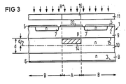
- FIG 3 shows a second semiconductor body of a thyristor.
- the same reference numerals used in this FIG 3 as in FIG 1 denote the same parts.
- the difference from the semiconductor body in FIG. 1 is that an auxiliary control electrode 20 is now arranged in the region of a lower breakdown voltage. The control electrode is not shown.
Landscapes
- Thyristors (AREA)
Abstract
Description
Die Erfindung betrifft ein Verfahren zum Herstellen eines Thyristors mit einem Halbleiterkörper, der einen Bereich enthält, der im Vergleich zum übrigen Halbleiterkörper eine geringere Durchbruchsspannung aufweist, wobei der Halbleiterkörper mindestens eine mit einer Steuerelektrode versehene erste Hauptfläche, eine zweite Hauptfläche und eine mit der Steuerelektrode verbundene erste Basiszone mit angrenzender zweiter Basiszone aufweist.The invention relates to a method for producing a thyristor with a semiconductor body which contains a region which has a lower breakdown voltage than the rest of the semiconductor body, the semiconductor body having at least one first main surface provided with a control electrode, a second main surface and one connected to the control electrode has first base zone with adjacent second base zone.
Solche Verfahren sind z.B. aus der DE-OS 23 00 754 bekannt und dienen dazu eine kontrollierbare Überkopfzündung des Thyristors in diesem Bereich bei der vorgegebenen geringeren Durchbruchspannung zu ermöglichen. Der Bereich, der im Vergleich zum übrigen Halbleiterkörper des Thyristors eine geringere Durchbruchsspannung aufweist, wird in dieser Veröffentlichung z. B. dadurch hergestellt, daß die zweite Basiszone in diesem Bereich dünner als außerhalb dieses Bereiches ausgebildet ist.Such methods are e.g. Known from DE-OS 23 00 754 and serve to enable controllable overhead ignition of the thyristor in this area at the predetermined lower breakdown voltage. The area which has a lower breakdown voltage compared to the other semiconductor body of the thyristor is described in this publication, for. B. manufactured in that the second base zone is thinner in this area than outside of this area.
In der DE-OS 23 46 205 ist beschrieben, den Bereich geringerer Durchbruchsspannung im Halbleiterkörper dadurch zu bilden, daß speziell solche Halbleiterscheiben als Ausgangsmaterial für den Halbleiterkörper ausgewählt werden, die in definierter Weise einen Bereich mit niedrigeren spezifischen Widerstand aufweisen. Solche Halbleiterscheiben lassen sich z.B. durch einen besonderen Silizium-Ziehprozeß herstellen.DE-OS 23 46 205 describes how to form the region of lower breakdown voltage in the semiconductor body by specifically selecting those semiconductor wafers as the starting material for the semiconductor body which have a region with a lower specific resistance in a defined manner. Such semiconductor wafers can e.g. using a special silicon drawing process.
Eine weitere Möglichkeit am Rand des Halbleiterkörpers einen Bereich anzuordnen, der im Vergleich zum übrigen Halbleiterkörper eine niedrigere Durchbruchsspannung aufweist, besteht z.B. darin, daß die Randkontur des Halbleiterkörpers mit einem negativen Winkel versehen wird.Another possibility of arranging an area at the edge of the semiconductor body which has a lower breakdown voltage compared to the rest of the semiconductor body is, for example, that the edge contour of the semiconductor body is provided with a negative angle.
Diese bekannten Verfahren haben den Nachteil, daß sie häufig nur mit unbefriedigender Ausbeute anzuwenden sind. Der Erfindung liegt die Aufgabe zugrunde, ein Verfahren anzugeben, mit dem es möglich ist, an einer bereits vorliegenden Thyristortablette nachträglich einen Bereich zu erzeugen, der im Vergleich zum übrigen Halbleiterkörper der Thryistortablette eine geringere Durchbruchsspannung aufweist.These known processes have the disadvantage that they can often only be used with an unsatisfactory yield. The invention is based on the object of specifying a method with which it is possible to subsequently generate an area on an already present thyristor tablet which has a lower breakdown voltage compared to the other semiconductor body of the thryristor tablet.
Diese Aufgabe wird dadurch gelöst, daß eine Hauptfläche des Halbleiterkörpers in diesen Bereich aus einer Protonenstrahlquelle mit Protonen bestrahlt wird, daß die Protonenenergie so bemessen wird, daß das Maximum der durch die Protonenbestrahlung erzeugten Störstellendichte und Dotierung zwischen dem pn-Übergang der ersten Basiszone und der zweiten Basiszone und der halben Dicke der zweiten Basiszone liegt, und daß der Halbleiterkörper nach der Protonenbestrahlung getempert wird.This object is achieved in that a main surface of the semiconductor body is irradiated with protons from a proton beam source in this area, that the proton energy is dimensioned such that the maximum of the impurity density and doping generated by the proton radiation between the pn junction of the first base zone and the second base zone and half the thickness of the second base zone, and that the semiconductor body is annealed after the proton irradiation.
Weiterbildungen der Erfindung sind Gegenstand der Unteransprüche.Developments of the invention are the subject of the dependent claims.
Besonders vorteilhaft bei unserem erfindungsgemäßen Verfahren ist, daß am bereits mit Elektroden versehenen Halbleiterkörper des Thyristors - also an der bereits fertiggestellten Thyristortablette - nachträglich ein Bereich gebildet werden kann, der im Vergleich zum übrigen Halbleiterkörper eine geringere Durchbruchsspannung aufweist. Beim lokalen Protonenbestrahlen ist nur eine Ausheiltemperatur von 250°C bis 350°C notwendig. Bei dieser niedrigen Temperatur wird der Halbleiterkörper mindestens zwei Stunden getempert. Durch diese niedrige Ausheiltemperatur wird wirksam verhindert, daß die am Halbleiterkörper bereits angebrachten Elektroden auf den Halbleiterkörper aufschmelzen oder die bereits am Halbleiterkörper angebrachte Passivierungsschicht beschädigt wird.It is particularly advantageous in our method according to the invention that an area can be subsequently formed on the semiconductor body of the thyristor which has already been provided with electrodes - that is to say on the already finished thyristor tablet - and which has a lower breakdown voltage compared to the other semiconductor body. With local proton irradiation, only a curing temperature of 250 ° C to 350 ° C is necessary. At this low temperature, the semiconductor body is annealed for at least two hours. This low annealing temperature effectively prevents the electrodes already attached to the semiconductor body from melting onto the semiconductor body or the passivation layer already attached to the semiconductor body from being damaged.
Das erfindungsgemäße Verfahren wird im folgenden anhand von drei Figuren näher erläutert. Es zeigen:
- FIG 1 einen ersten Halbleiterkörper eines Thyristors mit einem durch Protonenbestrahlung erzeugten Bereich niedrigerer Durchbruchspannung,
- FIG 2 die Feldstärkeverteilung E (x) im Bereich des Halbleiterkörpers längs der Achse II - II in FIG 1, und
- FIG 3 einen zweiten Halbleiterkörper eines Thyristors mit einem durch Protonenbestrahlung erzeugten Bereich niedrigerer Durchbruchsspannung,
- 1 shows a first semiconductor body of a thyristor with a region of lower breakdown voltage generated by proton radiation,
- 2 shows the field strength distribution E (x) in the region of the semiconductor body along the axis II-II in FIG. 1, and
- 3 shows a second semiconductor body of a thyristor with a region of lower breakdown voltage generated by proton radiation,
Der in FIG 1 dargestellte Halbleiterkörper 1 eines Thyristors weist zwischen seiner ersten Hauptfläche 2 und seiner zweiten Hauptfläche 3 mindestens teilweise vier Zonen jeweils abwechselnden Leitfähigkeitstyps auf. Die vier Zonen jeweils abwechselnden Leitfähigkeitstyps sind eine erste Emitterzone 7, eine an diese Emitterzone angrenzende erste Basiszone 9, eine mit dieser ersten Basiszone 9 einen pn-Übergang 15 bildende zweite Basiszone 10 mit der Dicke d, an die eine zweite Emitterzone 8 grenzt. Die erste Emitterzone 7, die in diesem Ausführungsbeispiel planar in die erste Basiszone 9 eingebettet ist, ist an der ersten Hauptfläche 2 mit einer ersten Emitterelektrode 5 verbunden. Die erste Basiszone 9 steht mit einer Steuerelektrode 4 in Kontakt, die ebenfalls an der Hauptfläche 2 angeordnet ist. Eine zweite Emitterelektrode 6 ist mit der zweiten Emitterzone 8 verbunden. In dem Beispiel nach FIG 1 ist die erste Emitterzone 7 und die zweite Basiszone 10 n-dotiert, während die erste Basiszone 9 und die zweite Emitterzone p-dotiert sind.The
Das erfindungsgemäße Verfahren sieht vor, in diesem Halbleiterkörper 1 einen Bereich zu bilden, der im Vergleich zum übrigen Halbleiterkörper 1 eine geringere Durchbruchsspannung aufweist. In dem in FIG 1 dargestellten Ausführungsbeispiel soll dieser Bereich niedrigerer Durchbruchsspannung in dem durch A gekennzeichneten Teil des Halbleiterkörpers 1 gebildet werden. Der übrige Teil des Halbleiterkörpers 1 ist mit B bezeichnet. Die Steuerelektrode 4 befindet sich in dem Ausführungsbeispiel nach FIG 1 innerhalb dieses Bereiches A des Halbleiterkörpers. Zur lokalen Protonenbestrahlung des Halbleiterkörpers 1 ist zwischen einer in der FIG. 1 nicht dargestellten Protonenstrahlquelle und der Hauptfläche 2 eine Abschirmvorrichtung 11 angeordnet. Die Abschirmvorrichtung 11 weist eine Öffnung 16 auf, durch die die Protonenstrahlung H⁺ allein den dafür vorgesehenen Bereich A der ersten Hauptfläche 2 des Halbleiterkörpers erreicht. Der Durchmesser der Öffnung 16 ist in diesem Beispiel etwas kleiner als der Durchmesser der Steuerelektrode 4 gewählt, so daß die erste Emitterzone 7 nicht mit Protonen bestrahlt wird. Die Protonenenergie wird so bemessen, daß das Maximum der durch die Protonenbestrahlung erzeugten Störstellendichte und Dotierung zwischen dem pn-Übergang 15 der ersten Basiszone 9 und der zweiten Basiszone 10 und der halben Dicke d/2 der zweiten Basiszone 10 liegt. Die Protonendosis wird so bemessen, daß die im Vergleich zum übrigen Halbleiterkörper B geforderte geringere Durchbruchsspannung im Bereich A erreicht wird. Nach der Protonenbestrahlung wird der Halbleiterkörper 1 getempert. Vorzugsweise geschieht dies mindestens zwei Stunden bei einer Temperatur zwischen 250°C und 350°C.The method according to the invention provides for forming a region in this
Die Protonendosis liegt an der Hauptfläche 2 vorteilhafterweise zwischen 10¹¹ und 10¹³ Protonen/cm², je nachdem, welche geforderte Durchbruchsspannung erreicht werden soll. Die Protonenenergie liegt zwischen 2 und 6 MeV.The proton dose on the
Sollen die Protonen in den Halbleiterkörper z. B. 200 µm eindringen, so ist eine Beschleunigungsenergie von etwa 5 MeV notwendig. Wie die Beschleunigungsenergie der Protonen von der Eindringtiefe abhängig ist, ist z.B. aus der US-PS 4 056 408 bekannt.Should the protons in the semiconductor body z. B. 200 microns penetrate, an acceleration energy of about 5 MeV is necessary. How the acceleration energy of the protons depends on the penetration depth is e.g. known from US-PS 4,056,408.
Durch die gewählte Protonenenergie der Protonenstrahlung wird also erreicht, daß die Protonen den pn-Übergang 15 durchdringen und kurz hinter diesem zur Ruhe kommen. In diesem Abbremsbereich 14 wird die größte Störstellendichte und Dotierung erzeugt. Seine Breite beträgt etwa 10 % der mittleren Eindringtiefe.The selected proton energy of the proton radiation ensures that the protons penetrate the
In FIG 2 ist die Feldstärkeverteilung im Bereich des Halbleiterkörpers 1 nach FIG 1 längs der eingezeichneten Achse II - II dargestellt. Die durch die Protonenbestrahlung erzeugte Dotierung führt zu einer Feldstärkeverteilung E (x) in der Raumladungszone, wie diese durch die durchgezogene Kurve 12 darge stellt ist. Die in FIG 2 dargestellte punktiert-strichlierte Kurve 13 zeigt die Feldstärkeverteilung E (x) im nicht mit Protonbestrahlung behandelten Halbleiterkörper 1. Im Abbremsbereich 14 ist der Feldstärkegradient nach der Poisson-Beziehung größer als im übrigen Teil der zweiten Basiszone 10. Dementsprechend wird die Durchbruchfeldstärke im Bereich A früher erreicht als im Bereich B. Durch die erfindungsgemäße Protonenbestrahlung dehnt sich zwar die Raumladungszone in der zweiten Basiszone 10 etwas weniger aus. Durch den damit größeren Abstand zur zweiten Emitterzone 8 wird zwar die Teiltransistorenverstärkung des Thyristors etwas vermindert und die Transistorsperrspannung angehoben. Dies wird jedoch durch ein erhöhtes Niveau der Ladungsträgergeneration im Abbremsbereich 14 ausgeglichen und überkompensiert.FIG. 2 shows the field strength distribution in the area of the
In FIG 3 ist ein zweiter Halbleiterkörper eines Thyristors dargestellt. Die in dieser FIG 3 verwendeten gleichen Bezugszeichen wie in FIG 1 bezeichnen gleiche Teile. Der Unterschied zum Halbleiterkörper in FIG 1 besteht darin, daß jetzt eine Hilfssteuerelektrode 20 im Bereich niedrigerer Durchbruchspannung angeordnet ist. Die Steuerelektrode ist nicht dargestellt.3 shows a second semiconductor body of a thyristor. The same reference numerals used in this FIG 3 as in FIG 1 denote the same parts. The difference from the semiconductor body in FIG. 1 is that an
Claims (7)
daß die Protonenenergie so bemessen wird, daß das Maximum der durch die Protonenbestrahlung erzeugten Störstellendichte und Dotierung zwischen dem pn-Übergang (15) der ersten Basiszone (9) und der zweiten Basiszone (10) und der halben Dicke d/2 der zweiten Basiszone (10) liegt,
daß der Halbleiterkörper (1) nach der Protonenbestrahlung getempert wird.1. A method for producing a thyristor having a semiconductor body (1) which contains an area (A) which has a lower breakdown voltage than the other semiconductor body, the semiconductor body (1) having at least one first main area provided with a control electrode (4) (2), has a second main surface (3) and a first base zone (9) connected to the control electrode (4) with an adjacent second base zone (10), characterized in that a main surface (2, 3) of the semiconductor body (1) in this area is irradiated with protons from a proton beam source,
that the proton energy is dimensioned such that the maximum of the impurity density and doping generated by the proton radiation between the pn junction (15) of the first base zone (9) and the second base zone (10) and half the thickness d / 2 of the second base zone ( 10) lies
that the semiconductor body (1) is annealed after proton irradiation.
Applications Claiming Priority (2)
| Application Number | Priority Date | Filing Date | Title |
|---|---|---|---|
| DE3817160 | 1988-05-19 | ||
| DE3817160 | 1988-05-19 |
Publications (1)
| Publication Number | Publication Date |
|---|---|
| EP0343369A1 true EP0343369A1 (en) | 1989-11-29 |
Family
ID=6354742
Family Applications (1)
| Application Number | Title | Priority Date | Filing Date |
|---|---|---|---|
| EP89106888A Withdrawn EP0343369A1 (en) | 1988-05-19 | 1989-04-18 | Process for manufacturing a thyristor |
Country Status (3)
| Country | Link |
|---|---|
| US (1) | US4987087A (en) |
| EP (1) | EP0343369A1 (en) |
| JP (1) | JPH0220024A (en) |
Cited By (11)
| Publication number | Priority date | Publication date | Assignee | Title |
|---|---|---|---|---|
| EP0423721A3 (en) * | 1989-10-16 | 1992-04-22 | Kabushiki Kaisha Toshiba | Semiconductor device with overvoltage protective function and method of fabricating such device |
| WO1992017907A1 (en) * | 1991-03-27 | 1992-10-15 | Siemens Aktiengesellschaft | Thyristor with adjustable breakover voltage, and a process for manufacturing it |
| US5243205A (en) * | 1989-10-16 | 1993-09-07 | Kabushiki Kaisha Toshiba | Semiconductor device with overvoltage protective function |
| WO1997002603A1 (en) * | 1995-07-03 | 1997-01-23 | Siemens Aktiengesellschaft | Thyristor with a layer of charge carriers having a reduced lifetime |
| DE19650762A1 (en) * | 1996-09-30 | 1998-07-02 | Eupec Gmbh & Co Kg | Thyristor with breakdown area |
| DE19711438A1 (en) * | 1997-03-19 | 1998-09-24 | Asea Brown Boveri | Thyristor with short turn-off time |
| DE10025567A1 (en) * | 2000-05-24 | 2001-12-06 | Infineon Technologies Ag | Production of deep-doped regions of one conductivity type in a semiconductor body with conductivity of the opposite type comprises inserting protons or hydrogen atoms in the direction of the current flow between the electrodes |
| US6373079B1 (en) | 1996-09-30 | 2002-04-16 | Eupec Europaeische Gesellschaft Fur Leistungshalbleiter Mbh+Co.Kg | Thyristor with breakdown region |
| DE10243758A1 (en) * | 2002-09-20 | 2004-04-01 | eupec Europäische Gesellschaft für Leistungshalbleiter mbH | Method for producing a buried stop zone in a semiconductor component and semiconductor component with a buried stop zone |
| DE10344592B4 (en) * | 2003-09-25 | 2006-01-12 | eupec Europäische Gesellschaft für Leistungshalbleiter mbH | A method of adjusting the breakdown voltage of a thyristor having a breakdown structure |
| RU2410795C1 (en) * | 2009-07-22 | 2011-01-27 | Открытое акционерное общество "Электровыпрямитель" | Power semiconductor device with controlled switching voltage |
Families Citing this family (19)
| Publication number | Priority date | Publication date | Assignee | Title |
|---|---|---|---|---|
| US5510274A (en) * | 1987-08-19 | 1996-04-23 | Mitsubishi Denki Kabushiki Kaisha | Method of controlling a carrier lifetime in a semiconductor switching device |
| EP0398120B1 (en) * | 1989-05-18 | 1993-10-13 | Asea Brown Boveri Ag | Semiconductor device |
| US5284780A (en) * | 1989-09-28 | 1994-02-08 | Siemens Aktiengesellschaft | Method for increasing the electric strength of a multi-layer semiconductor component |
| JPH0650738B2 (en) * | 1990-01-11 | 1994-06-29 | 株式会社東芝 | Semiconductor device and manufacturing method thereof |
| JPH03111230U (en) * | 1990-02-27 | 1991-11-14 | ||
| US5240865A (en) * | 1990-07-30 | 1993-08-31 | Texas Instruments Incorporated | Method of forming a thyristor on an SOI substrate |
| DE19649800A1 (en) * | 1996-12-02 | 1998-06-04 | Asea Brown Boveri | Method for producing a turn-off thyristor with an anode-side stop layer and a transparent anode emitter |
| US6114225A (en) * | 1998-11-16 | 2000-09-05 | Industrial Technology Research Institute | Local penetrating proton beam transmutation doping method for silicon |
| US6214750B1 (en) | 1999-01-04 | 2001-04-10 | Industrial Technology Research Institute | Alternative structure to SOI using proton beams |
| DE50015361D1 (en) * | 1999-02-22 | 2008-10-30 | Infineon Technologies Ag | METHOD FOR ADJUSTING THE BREAKTHROUGH VOLTAGE OF A THYRISTOR |
| US6723586B1 (en) * | 1999-06-08 | 2004-04-20 | Siemens Aktiengesellschaft | Thyristor provided with integrated circuit-commutated recovery time protection and production method therefor |
| US7205632B2 (en) * | 2004-04-05 | 2007-04-17 | Taiwan Semiconductor Manufacturing Company, Ltd. | Anti-scattering attenuator structure for high energy particle radiation into integrated circuits |
| US7492018B2 (en) * | 2004-09-17 | 2009-02-17 | Taiwan Semiconductor Manufacturing Company, Ltd. | Isolating substrate noise by forming semi-insulating regions |
| DE102005007599B3 (en) * | 2005-02-18 | 2006-05-11 | Infineon Technologies Austria Ag | Field stop zone producing method for e.g. bipolar transistor, involves subjecting semiconductor body to rapid thermal annealing process in nitrating atmosphere, before irradiation process of body |
| DE102005009020B4 (en) * | 2005-02-28 | 2012-04-26 | Infineon Technologies Austria Ag | Method for generating a power transistor and thus generated integrated circuit arrangement |
| US7687841B2 (en) * | 2005-08-02 | 2010-03-30 | Micron Technology, Inc. | Scalable high performance carbon nanotube field effect transistor |
| RU2474926C1 (en) * | 2011-09-21 | 2013-02-10 | Российская Федерация, От Имени Которой Выступает Министерство Промышленности И Торговли Российской Федерации | Method to control voltage of power semiconductor instrument switching |
| CN105448900B (en) * | 2015-01-26 | 2019-02-26 | 湖北台基半导体股份有限公司 | A kind of high frequency low voltage drop power semiconductor modular |
| CN117524859A (en) * | 2023-11-21 | 2024-02-06 | 国电投核力创芯(无锡)科技有限公司 | A masking method for wafer proton irradiation |
Citations (5)
| Publication number | Priority date | Publication date | Assignee | Title |
|---|---|---|---|---|
| EP0014516A1 (en) * | 1979-01-04 | 1980-08-20 | Westinghouse Electric Corporation | Forming irradiated regions in semiconductor bodies by nuclear radiation |
| DE3117202A1 (en) * | 1981-04-30 | 1982-11-18 | Brown, Boveri & Cie Ag, 6800 Mannheim | Method of adjusting the lifetime of minority charge carriers in semiconductor switches by proton irradiation |
| DE3339393A1 (en) * | 1983-10-29 | 1985-05-09 | Licentia Patent-Verwaltungs-Gmbh, 6000 Frankfurt | Process for producing an n-doped zone underneath an outer highly doped zone in a semiconductor structure |
| DE3733100A1 (en) * | 1986-10-01 | 1988-04-14 | Mitsubishi Electric Corp | GATE SHUT-OFF THYRISTOR |
| EP0297325A2 (en) * | 1987-07-01 | 1989-01-04 | Mitsubishi Denki Kabushiki Kaisha | Gate turn-off thyristor and manufacturing method thereof |
Family Cites Families (5)
| Publication number | Priority date | Publication date | Assignee | Title |
|---|---|---|---|---|
| DE2140993C3 (en) * | 1971-08-16 | 1979-06-21 | Siemens Ag, 1000 Berlin Und 8000 Muenchen | Thyristor |
| DE2300754A1 (en) * | 1973-01-08 | 1974-07-11 | Siemens Ag | THYRISTOR |
| US3990091A (en) * | 1973-04-25 | 1976-11-02 | Westinghouse Electric Corporation | Low forward voltage drop thyristor |
| US4056408A (en) * | 1976-03-17 | 1977-11-01 | Westinghouse Electric Corporation | Reducing the switching time of semiconductor devices by nuclear irradiation |
| US4311534A (en) * | 1980-06-27 | 1982-01-19 | Westinghouse Electric Corp. | Reducing the reverse recovery charge of thyristors by nuclear irradiation |
-
1989
- 1989-04-18 EP EP89106888A patent/EP0343369A1/en not_active Withdrawn
- 1989-05-05 US US07/348,231 patent/US4987087A/en not_active Expired - Fee Related
- 1989-05-15 JP JP1121305A patent/JPH0220024A/en active Pending
Patent Citations (5)
| Publication number | Priority date | Publication date | Assignee | Title |
|---|---|---|---|---|
| EP0014516A1 (en) * | 1979-01-04 | 1980-08-20 | Westinghouse Electric Corporation | Forming irradiated regions in semiconductor bodies by nuclear radiation |
| DE3117202A1 (en) * | 1981-04-30 | 1982-11-18 | Brown, Boveri & Cie Ag, 6800 Mannheim | Method of adjusting the lifetime of minority charge carriers in semiconductor switches by proton irradiation |
| DE3339393A1 (en) * | 1983-10-29 | 1985-05-09 | Licentia Patent-Verwaltungs-Gmbh, 6000 Frankfurt | Process for producing an n-doped zone underneath an outer highly doped zone in a semiconductor structure |
| DE3733100A1 (en) * | 1986-10-01 | 1988-04-14 | Mitsubishi Electric Corp | GATE SHUT-OFF THYRISTOR |
| EP0297325A2 (en) * | 1987-07-01 | 1989-01-04 | Mitsubishi Denki Kabushiki Kaisha | Gate turn-off thyristor and manufacturing method thereof |
Non-Patent Citations (1)
| Title |
|---|
| PATENT ABSTRACTS OF JAPAN, Band 12, Nr. 106 (E-596)[2953], 6. April 1988; & JP-A-62 235 782 (TOYOTA CENTRAL RES. & DEV. LAB. INC.) 15-10-1987 * |
Cited By (14)
| Publication number | Priority date | Publication date | Assignee | Title |
|---|---|---|---|---|
| US5243205A (en) * | 1989-10-16 | 1993-09-07 | Kabushiki Kaisha Toshiba | Semiconductor device with overvoltage protective function |
| EP0423721A3 (en) * | 1989-10-16 | 1992-04-22 | Kabushiki Kaisha Toshiba | Semiconductor device with overvoltage protective function and method of fabricating such device |
| WO1992017907A1 (en) * | 1991-03-27 | 1992-10-15 | Siemens Aktiengesellschaft | Thyristor with adjustable breakover voltage, and a process for manufacturing it |
| US5420045A (en) * | 1991-03-27 | 1995-05-30 | Siemens Aktiengesellschaft | Process for manufacturing thyristor with adjustable breakover voltage |
| WO1997002603A1 (en) * | 1995-07-03 | 1997-01-23 | Siemens Aktiengesellschaft | Thyristor with a layer of charge carriers having a reduced lifetime |
| US6373079B1 (en) | 1996-09-30 | 2002-04-16 | Eupec Europaeische Gesellschaft Fur Leistungshalbleiter Mbh+Co.Kg | Thyristor with breakdown region |
| DE19650762A1 (en) * | 1996-09-30 | 1998-07-02 | Eupec Gmbh & Co Kg | Thyristor with breakdown area |
| DE19711438A1 (en) * | 1997-03-19 | 1998-09-24 | Asea Brown Boveri | Thyristor with short turn-off time |
| DE10025567A1 (en) * | 2000-05-24 | 2001-12-06 | Infineon Technologies Ag | Production of deep-doped regions of one conductivity type in a semiconductor body with conductivity of the opposite type comprises inserting protons or hydrogen atoms in the direction of the current flow between the electrodes |
| DE10025567C2 (en) * | 2000-05-24 | 2003-03-27 | Infineon Technologies Ag | Method for producing deeply doped areas in a semiconductor body |
| DE10243758A1 (en) * | 2002-09-20 | 2004-04-01 | eupec Europäische Gesellschaft für Leistungshalbleiter mbH | Method for producing a buried stop zone in a semiconductor component and semiconductor component with a buried stop zone |
| US7749876B2 (en) | 2002-09-20 | 2010-07-06 | Infineon Technologies Ag | Method for the production of a buried stop zone in a semiconductor component and semiconductor component comprising a buried stop zone |
| DE10344592B4 (en) * | 2003-09-25 | 2006-01-12 | eupec Europäische Gesellschaft für Leistungshalbleiter mbH | A method of adjusting the breakdown voltage of a thyristor having a breakdown structure |
| RU2410795C1 (en) * | 2009-07-22 | 2011-01-27 | Открытое акционерное общество "Электровыпрямитель" | Power semiconductor device with controlled switching voltage |
Also Published As
| Publication number | Publication date |
|---|---|
| JPH0220024A (en) | 1990-01-23 |
| US4987087A (en) | 1991-01-22 |
Similar Documents
| Publication | Publication Date | Title |
|---|---|---|
| EP0343369A1 (en) | Process for manufacturing a thyristor | |
| DE102007026387B4 (en) | Method for producing a semiconductor device | |
| DE112011105826B4 (en) | Semiconductor device and method of making the same | |
| DE19704996A1 (en) | Process for the production of IGBT components | |
| DE3124988C2 (en) | ||
| DE2812740A1 (en) | METHOD OF MANUFACTURING A VERTICAL BIPOLAR INTEGRATED CIRCUIT | |
| EP1611613B2 (en) | Method for producing a semiconductor component | |
| DE102018205274A1 (en) | SEMICONDUCTOR DEVICE AND METHOD FOR THE PRODUCTION THEREOF | |
| DE2354523C3 (en) | Process for the production of electrically insulating blocking regions in semiconductor material | |
| DE2050497A1 (en) | Process for increasing the diffusion of atoms into a heated substrate by means of bombardment | |
| EP0833388A2 (en) | Amplifying gate thyristor with lateral resistance | |
| DE2262024A1 (en) | METHOD FOR MANUFACTURING SEMI-CONDUCTOR COMPONENTS OR SEMICONDUCTOR CIRCUITS | |
| DE3889354T2 (en) | Semiconductor device. | |
| DE10240107B4 (en) | Edge termination for power semiconductor device and for diode and method for producing an n-type region for such edge termination | |
| WO2001024276A1 (en) | Semiconductor assembly with charge compensation | |
| DE1544275B2 (en) | PROCESS FOR THE FORMATION OF ZONES OF DIFFERENT CONDUCTIVITY IN SEMICONDUCTOR CRYSTALS BY ION IMPLANTATION | |
| EP0931351B1 (en) | Thyristor with breakdown region | |
| DE69719527T2 (en) | METHOD FOR DOPING A AREA WITH BOR IN A SiC LAYER | |
| EP0332955A2 (en) | Thyristor having a large forward and reverse blocking capability, and method of making the same | |
| DE102004039208B4 (en) | Method for producing a power device with a buried n-doped semiconductor zone and power device | |
| DE2951916A1 (en) | LIGHT CONTROLLED THYRISTOR | |
| DE68913109T2 (en) | Method of manufacturing a control and protection diode. | |
| DE2837762C2 (en) | Process for making triacs | |
| EP0577623B1 (en) | Method of making a thyristor with adjustable breakover voltage | |
| EP0776028B1 (en) | Process for reducing the carrier charge concentration for lowering the storage charge in semiconductor devices through two implantation steps |
Legal Events
| Date | Code | Title | Description |
|---|---|---|---|
| PUAI | Public reference made under article 153(3) epc to a published international application that has entered the european phase |
Free format text: ORIGINAL CODE: 0009012 |
|
| AK | Designated contracting states |
Kind code of ref document: A1 Designated state(s): CH DE FR GB IT LI SE |
|
| 17P | Request for examination filed |
Effective date: 19891219 |
|
| STAA | Information on the status of an ep patent application or granted ep patent |
Free format text: STATUS: THE APPLICATION IS DEEMED TO BE WITHDRAWN |
|
| 18D | Application deemed to be withdrawn |
Effective date: 19921103 |