EP0330141B1 - Vorrichtung und Verfahren zum Kristallziehen - Google Patents
Vorrichtung und Verfahren zum Kristallziehen Download PDFInfo
- Publication number
- EP0330141B1 EP0330141B1 EP89102992A EP89102992A EP0330141B1 EP 0330141 B1 EP0330141 B1 EP 0330141B1 EP 89102992 A EP89102992 A EP 89102992A EP 89102992 A EP89102992 A EP 89102992A EP 0330141 B1 EP0330141 B1 EP 0330141B1
- Authority
- EP
- European Patent Office
- Prior art keywords
- crucible
- material melt
- melt
- crystal
- crystal pulling
- Prior art date
- Legal status (The legal status is an assumption and is not a legal conclusion. Google has not performed a legal analysis and makes no representation as to the accuracy of the status listed.)
- Expired - Lifetime
Links
Images


Classifications
-
- C—CHEMISTRY; METALLURGY
- C30—CRYSTAL GROWTH
- C30B—SINGLE-CRYSTAL GROWTH; UNIDIRECTIONAL SOLIDIFICATION OF EUTECTIC MATERIAL OR UNIDIRECTIONAL DEMIXING OF EUTECTOID MATERIAL; REFINING BY ZONE-MELTING OF MATERIAL; PRODUCTION OF A HOMOGENEOUS POLYCRYSTALLINE MATERIAL WITH DEFINED STRUCTURE; SINGLE CRYSTALS OR HOMOGENEOUS POLYCRYSTALLINE MATERIAL WITH DEFINED STRUCTURE; AFTER-TREATMENT OF SINGLE CRYSTALS OR A HOMOGENEOUS POLYCRYSTALLINE MATERIAL WITH DEFINED STRUCTURE; APPARATUS THEREFOR
- C30B15/00—Single-crystal growth by pulling from a melt, e.g. Czochralski method
- C30B15/10—Crucibles or containers for supporting the melt
- C30B15/12—Double crucible methods
-
- C—CHEMISTRY; METALLURGY
- C30—CRYSTAL GROWTH
- C30B—SINGLE-CRYSTAL GROWTH; UNIDIRECTIONAL SOLIDIFICATION OF EUTECTIC MATERIAL OR UNIDIRECTIONAL DEMIXING OF EUTECTOID MATERIAL; REFINING BY ZONE-MELTING OF MATERIAL; PRODUCTION OF A HOMOGENEOUS POLYCRYSTALLINE MATERIAL WITH DEFINED STRUCTURE; SINGLE CRYSTALS OR HOMOGENEOUS POLYCRYSTALLINE MATERIAL WITH DEFINED STRUCTURE; AFTER-TREATMENT OF SINGLE CRYSTALS OR A HOMOGENEOUS POLYCRYSTALLINE MATERIAL WITH DEFINED STRUCTURE; APPARATUS THEREFOR
- C30B15/00—Single-crystal growth by pulling from a melt, e.g. Czochralski method
- C30B15/02—Single-crystal growth by pulling from a melt, e.g. Czochralski method adding crystallising materials or reactants forming it in situ to the melt
- C30B15/04—Single-crystal growth by pulling from a melt, e.g. Czochralski method adding crystallising materials or reactants forming it in situ to the melt adding doping materials, e.g. for n-p-junction
-
- C—CHEMISTRY; METALLURGY
- C30—CRYSTAL GROWTH
- C30B—SINGLE-CRYSTAL GROWTH; UNIDIRECTIONAL SOLIDIFICATION OF EUTECTIC MATERIAL OR UNIDIRECTIONAL DEMIXING OF EUTECTOID MATERIAL; REFINING BY ZONE-MELTING OF MATERIAL; PRODUCTION OF A HOMOGENEOUS POLYCRYSTALLINE MATERIAL WITH DEFINED STRUCTURE; SINGLE CRYSTALS OR HOMOGENEOUS POLYCRYSTALLINE MATERIAL WITH DEFINED STRUCTURE; AFTER-TREATMENT OF SINGLE CRYSTALS OR A HOMOGENEOUS POLYCRYSTALLINE MATERIAL WITH DEFINED STRUCTURE; APPARATUS THEREFOR
- C30B15/00—Single-crystal growth by pulling from a melt, e.g. Czochralski method
- C30B15/20—Controlling or regulating
-
- C—CHEMISTRY; METALLURGY
- C30—CRYSTAL GROWTH
- C30B—SINGLE-CRYSTAL GROWTH; UNIDIRECTIONAL SOLIDIFICATION OF EUTECTIC MATERIAL OR UNIDIRECTIONAL DEMIXING OF EUTECTOID MATERIAL; REFINING BY ZONE-MELTING OF MATERIAL; PRODUCTION OF A HOMOGENEOUS POLYCRYSTALLINE MATERIAL WITH DEFINED STRUCTURE; SINGLE CRYSTALS OR HOMOGENEOUS POLYCRYSTALLINE MATERIAL WITH DEFINED STRUCTURE; AFTER-TREATMENT OF SINGLE CRYSTALS OR A HOMOGENEOUS POLYCRYSTALLINE MATERIAL WITH DEFINED STRUCTURE; APPARATUS THEREFOR
- C30B29/00—Single crystals or homogeneous polycrystalline material with defined structure characterised by the material or by their shape
- C30B29/02—Elements
- C30B29/06—Silicon
-
- H—ELECTRICITY
- H10—SEMICONDUCTOR DEVICES; ELECTRIC SOLID-STATE DEVICES NOT OTHERWISE PROVIDED FOR
- H10P—GENERIC PROCESSES OR APPARATUS FOR THE MANUFACTURE OR TREATMENT OF DEVICES COVERED BY CLASS H10
- H10P10/00—Bonding of wafers, substrates or parts of devices
-
- Y—GENERAL TAGGING OF NEW TECHNOLOGICAL DEVELOPMENTS; GENERAL TAGGING OF CROSS-SECTIONAL TECHNOLOGIES SPANNING OVER SEVERAL SECTIONS OF THE IPC; TECHNICAL SUBJECTS COVERED BY FORMER USPC CROSS-REFERENCE ART COLLECTIONS [XRACs] AND DIGESTS
- Y10—TECHNICAL SUBJECTS COVERED BY FORMER USPC
- Y10T—TECHNICAL SUBJECTS COVERED BY FORMER US CLASSIFICATION
- Y10T117/00—Single-crystal, oriented-crystal, and epitaxy growth processes; non-coating apparatus therefor
- Y10T117/10—Apparatus
- Y10T117/1024—Apparatus for crystallization from liquid or supercritical state
- Y10T117/1032—Seed pulling
- Y10T117/1052—Seed pulling including a sectioned crucible [e.g., double crucible, baffle]
Definitions
- This invention relates to a method for pulling semiconductor crystal such as silicon crystal and, more particularly, to an apparatus having a double structure crucible which is divided into inner and outer chambers, and a method for controlling the resistivity and other crystal characteristics by means of the crystal pulling apparatus.
- the impurity concentration distribution in the longitudinal direction of the grown single crystal varies significantly, as a result of which, the yield of single crystal having the desired impurity concentration range (or resistivity range when the impurity is an electrically active material; i.e. the conductive impurity) may be significantly reduced.
- inner crucible 2 is arranged as a floating crucible inside outer crucible 1, with small hole 3 being formed in the bottom of inner crucible 2.
- the balance between the buoyancy of inner crucible 2 and the force of gravity is utilized to maintain the surface level h of the melt in the inner crucible.
- the outer crucible is raised relative to the fixed inner crucible, so as to supply melt 5 from the outer crucible to the inner crucible in such a way that the surface level h of the melt in the inner crucible is kept constant.
- the impurity concentration of melt 5 in the outer crucible is Co
- the impurity concentration of melt 4 in the inner crucible is Co/k (k being the segregation coefficient)
- the concentration of impurity taken into pulling crystal 6 becomes Co, thus ensuring that the melt (pure silicon or germanium) and the impurity used for growing the crystal are always supplied in equal amounts from melt 5 in the outer crucible to melt 4 in the inner crucible.
- the impurity concentration of melt 4 in the inner crucible is kept at Co/k, and thus the impurity concentration of pulling crystal 6 is kept at constant value Co.
- the impurity concentration cannot be kept constant, and thus the impurity concentration of crystal 6 will vary (i.e. increase) as the solidification ratio increases. More precisely, the impurity concentration can be kept constant only within the following range of the solidification ratio G: 0 ⁇ G ⁇ 1 - (h/H) (1) where H is the initial surface level of the melt in the outer crucible, and h is the surface level of the melt in the inner crucible, to be kept constant during the pulling process).
- the resistivity can be kept constant only when the solidification ratio is less than 0.6 to 0.7, the resistivity varying significantly after the solidification ratio becomes higher than this value.
- Another single crystal growing method is the floating zone technique (FZ technique), and according to this technique, it is possible to grow a rod-like single crystal having a constant impurity concentration in the longitudinal direction.
- FZ technique floating zone technique
- the distribution of the dopant impurity in the radial cross section of a single crystal obtained by way of the FZ technique is non-uniform in comparison with a single crystal obtained by way of the CZ technique.
- the in-plane distribution ⁇ of resistivity ⁇ attained by resistivity measurement using four probes is 6 to 15% when the CZ technique is used, but reaches as high as 20 to 50% when the FZ technique is used.
- ⁇ ( ⁇ max - ⁇ min )/ ⁇ min , the in-plane resistance variation ⁇ SR caused by the spreading resistance measurement being 10 to 20% in the CZ crystal, but reaching as high as 30 to 50% in the FZ crystal.
- An object of this invention is to provide a crystal pulling apparatus by means of which the radial-direction resistivity of a grown semiconductor single crystal is relatively constant and the resistivity in the longitudinal direction thereof or the resistivity and other characteristics can be controlled.
- Another object of this invention is to provide a crystal pulling method for growing a single crystal whose resistivity, for example, can be set within a desired range at high yield.
- a crystal pulling apparatus having an integral type double crucible comprises a cylindrical separator wall (14) which is disposed in and is coaxial with a crucible (11) containing semiconductor material melt to divide the crucible (11) into inner and outer chambers (20, 21).
- a small hole (15) is formed in the separator wall (14), and a coupling tube (16) for connecting the inner chamber to the outer chamber, for example, a pipe-like passage supplied with the small hole (15), is provided. While crystal is pulled and grown from the melt in the inner chamber (20) which has an impurity composition different from that of the melt in the outer chamber (21), material melt in the outer chamber (21) is being supplied to the inner chamber (20) via the coupling tube (16).
- the length L of the coupling tube in this invention is set to satisfy the condition b > L ⁇ 4a, where a is an inner diameter of the coupling tube (16), and b is an inner peripheral length (2 ⁇ r) of the inner chamber (20).
- a is an inner diameter of the coupling tube (16)
- b is an inner peripheral length (2 ⁇ r) of the inner chamber (20).
- the minor axis thereof is used as inner diameter a , and then the condition b > L ⁇ 4a can be applied. Further, in a case where the inner diameter of the tube (16) is not constant (for example, tapered form), the average of the inner diameter over the entire length L is used as inner diameter a.
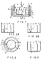
- Fig. 1 shows a crystal pulling apparatus used in one embodiment of this invention.
- a container of a pulling device for containing a hot zone including the crucible, a heat reserving cylinder and the like, which are well known in the art, are omitted here.
- Fig. 1 12 denotes a graphite crucible mounted on vertically movable and rotatable crucible shaft 13, and 11 denotes an outer crucible formed of a quartz cylindrical container disposed in contact with the inner surface of graphite crucible 12.
- Outer crucible 11 is reinforced (or supported) by means of graphite crucible 12.
- Outer crucible 11 is heated by means of heater 10 disposed around crucible 11.
- Separator wall 14 formed of a quartz cylindrical container is disposed in outer crucible 11.
- Separator wall penetrating hole 15 is formed in separator wall 14, and quartz pipe-like coupling tube 16 which is supplied with hole 15 is mounted on wall 14.
- Cylindrical separator wall 14 is fixed by fusion on the inner bottom surface of outer crucible 14.
- the inner space of separator wall 14 constitutes inner chamber 20 for receiving melt ML1 and a space between separator wall 14 and outer crucible 11 constitutes outer chamber 21 for receiving melt ML2.
- Fig. 2 is a plan view of crucible 11 of the apparatus shown in Fig. 1 in which separator wall 14 is fixed by fusion.
- coupling tube 16 connects the inside of separator wall 14 to outer chamber 21 via small hole 15.
- Coupling tube 16 is mounted on the curved outer surface portion of separator wall 14 and fixed by fusion thereto, as shown by Figs. 2A and 2B.
- separation wall 14 can be formed in the cylindrical form as shown in Figs. 1 and 2.
- coupling tube 16 is formed in conjunction with the inner portion of penetration hole 15 of separation wall 14 or inner chamber 20.
- the ratio r/R of inner diameter 2r of inner crucible 24 and inner diameter 2R of outer crucible 11 of Fig. 3 can be varied in actual use. For this reason, it is effective to removably and coaxially mount inner crucible 24 on outer crucible 11 with the bottoms thereof set in contact with each other by means of a jig or the like, instead of fixing them together by fusion.
- inner crucible 24b shown in Fig. 4A and outer crucible 11a shown in Fig. 4B can be combined.
- Inner crucible 24b has three or more positioning rods 24a which radially extend from the upper end with the tip ends thereof set in contact with the inner wall of the inner crucible. Then, as shown in Fig.
- crucible 11a can be removably and coaxially mounted on crucible 24a with the bottoms thereof set in contact with each other. It is also possible to place positioning rods 24c shown in Fig. 4D on upper end 11b of outer crucible 11a so as to removably mount the inner crucible on the outer crucible. Further, as shown in Fig. 4E, it is also possible to place positioning rods 24d by use of guide rods 11d set on upper end 11b of outer crucible 11a so as to removably mount the inner crucible on the outer crucible.
- Fig. 5 shows the result of experiment indicating the effect of impurity outflow suppression attained when inner diameter a and length L of coupling tube 16 are changed.
- the experiment was effected to check P concentration Cin in the inner crucible and P concentration Cout in the outer crucible after the melt process was completed under the condition that the outer crucible of 35,56cm (14") ⁇ and inner crucible of 20,32cm (8") ⁇ , silicon material charge amount of 20 kg and crucible rotation of 8 rpm were used, and then phosphorus (P) was doped into the inner crucible and the crucible was continuously rotated for two hours.
- the ratio Cout/Cin is shown in the ordinate when L/a (abscissa) is varied from 1 to 32 with inner diameter a set to 2 mm, 3 mm and 6 mm.
- Fig. 6 shows the ratios Cout/Cin obtained by using the same crucible as used in the case of Fig. 5 and the same melt amount and dope amount as used in the case of Fig. 5.
- the ratios Cout/Cin are obtained after two hours have passed from the P doping in the melt with the rotation speed of inner crucible 11, having the coupling tube with the inner diameter a of 6 mm, set to 0 rpm, 3 rpm, and 8 rpm.
- the ratio Cout/Cin is obtained in condition that the rotation speed of inner crucible 11 is set to 0 rpm and the vertical magneticc field of more than 0.15T (1500 gauss) is applying.
- the magnetic field can be applied by use of electromagnet EM which is mounted to surround crucible 11 as shown in Fig. 16, for example.
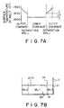
- Fig. 7A shows the distribution of surface temperature of silicon melt in outer chamber 21 and inner chamber 20 in the silicon single crystal pulling process.
- projection crystal 20a grows from separation wall 14 as shown in Fig. 7B.
- ⁇ T was set to be 5°C and 10°C
- the projection crystal was observed in all the five experiments.
- ⁇ T was set to be 15°C
- the projection crystal was observed in two out of five experiments and was not observed in the remaining three experiments.
- ⁇ T was set to be 20°C, the projection crystal was observed in one out of five experiments and was not observed in the remaining four experiments.
- the number of chambers for receiving material melt in the integral type double crucible is two which is different from that (one) used in the conventional CZ technique but is the same as that (two) used in the conventional floating type double crucible.
- the inner and outer chambers are arranged in upper and lower positions respectively.
- inner chamber 20 and outer chamber 21 are arranged in substantially the same height level.
- the surface level of the melt in the inner crucible is kept constant as described before.
- the surface level of melt ML1 subjected to the pulling process in the inner chamber is set substantially equal to that of melt ML2 in the outer chamber by means of coupling tube 16.
- the surface level of melt ML1 in the inner chamber during the crystal pulling process is gradually lowered and cannot be kept constant.
- the feature of the integral type double crucible of this invention resides in that inner chamber 20 and outer chamber 21 are divided by concentric cylindrical separation wall 14 and coupling tube 16 is provided to suppress outflow of impurity from inner chamber 20 to outer chamber 21.
- the feature can be attained irrespective of the fact that the surface level of melt ML1 in the inner chamber is set equal to that of melt ML2 in the outer chamber and the surface level of melt subjected to the pulling process in the inner chamber is kept constant.
- melt ML2 in the outer chamber of the crucible of a crystal pulling apparatus of the construction shown in Fig. 1 is undoped
- the inner diameter of outer crucible 11 is 2R
- the inner diameter of separation wall 14 is 2r.
- the segregation of dopant impurity in crystal 17 pulled from doped melt ML1 in inner chamber 20 is determined based on apparent segregation coefficient k eff which can be expressed as follows.
- k eff (R/r)2k (2) Since segregation coefficient k of general impurity is less than 1 (for example, k of P, B and Si is 0.35, 0.80, and 0.023), it is possible to set k eff to a value which is equal to or near 1 by selectively setting inner diameter 2r of separation wall 14 to a proper value. k eff of 1 means that the impurity concentration (resistivity in the case of low resistance) in a longitudinal direction of the crystal is constant.
- inner diameter a and length L of coupling tube 16 were respectively set to be 4 mm and 50 mm.
- outer chamber 11 of 30,48cm (12") ⁇ with the silicon charge amount of 14 kg was used
- inner radius r of cylindrical separation wall 14 was set to be approx. 0.6R ( ⁇ k ⁇ 0.6 because segregation coefficient k of P is 0.35)
- silicon single crystal with resistivity of 5 to 6 ⁇ ⁇ cm, 10,16cm (4") ⁇ , and growth orientation (111) was grown by use of material melt ML1 doped with P in the same manner as in the CZ technique.
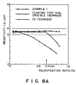
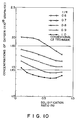
- FIGs. 8A and 8B shows the relation between the solidification ratio (abscissa) and the resistivity (ordinate) of the crystal obtained in this embodiment by mark ⁇ together with those obtained by the conventional floating type dual crucible method (by mark ⁇ ) and conventional CZ technique (mark ⁇ ).
- the solidification ratio In order to obtain wafers within such a narrow resistivity range, the solidification ratio must be less than 30% in the conventional CZ technique and less than 60% (less than the solidification ratio of 1-h/H) in the conventional floating type double crucible method.
- the narrow resistivity range can be obtained in the entire length of the single crystal.
- the in-plane resistivity distribution ⁇ of the wafer obtained in this embodiment was 6 to 15%, superior to that of the wafer attained by the FZ technique which is 15 to 50%, and substantially the same as that of the wafer attained by the CZ technique.
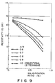
- the requirements for the quality of crystal include not only the resistivity range but also the oxygen concentration range.
- the concentrations of oxygen and conductive impurity P are controlled within the range of P doped resistivity of 7.5 to 12 ⁇ ⁇ cm and the range of oxygen concentration of 1.45 to 1.85 ⁇ 1018 atoms/cm3.
- the oxygen concentration becomes high when a relatively large crystal is pulled from a small crucible.
- the measurement was made to check the relations of the resistivity (Fig. 9) and the oxygen concentration (Fig. 10) with respect to the solidification ratio with the ratio r/R set at 0.6, 0.7, 0.8, 0.9 and 1.0 (the case wherein the ratio r/R is set at 1.0 corresponds to the ordinary CZ technique in which no double crucible is used).
- the yield relating to the resistivity which is represented by the yield of effective material expressed by (the weight of specified good article)/(specification-free possible weight) shown in Table 1 was obtained.
- Table 1 r/R 0.6 0.7 0.8 0.9 1.0 Yield of Effective Material (%) 100 90.7 71.9 61.6 56.8
- the ratio r/R is selectively set based on not only impurity such as oxygen which is different from the dopant but also the crystal growing condition.
- crucible 20 of a diameter which is relatively large (preferably more than twice) with respect to that of crystal 17 is used, crystal of good quality can be easily obtained. Therefore, in a case where it is permitted to set the resistivity within a certain desired range, crystal of good quality can be easily grown by setting r to be as large as possible within the range of k eff corresponding to the desired resistivity range.
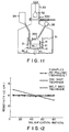
- Fig. 11 is a conceptional view of the apparatus used in embodiment 3.
- 31 denotes an integral type double crucible of 40,64cm (16") ⁇ which can receive melt of 35 kg.
- the crucible includes cylindrical separation wall 14 of 25,4cm (10") ⁇ (because of phosphorus doping, the value of 25,4cm/40,64cm (10"/16") is set substantially equal to root mean square ⁇ k( ⁇ 0.6) of segregation coefficient k), and coupling tube 16 having inner diameter a of 6 mm and length L of 100 mm.
- 32 denotes crystal in which dislocation has erroneously occurred, 33 a pull chamber which can be separated by means of gate valve 33a, 34 a hopper for introducing undoped material 34x, and 35 a supply unit for introducing doped material 35x.
- melt ML1 in the inner chamber is Co and melt ML2 in the outer chamber is undoped. Since dislocation occurred in crystal 32 when crystal 32 of 12,7cm (5") ⁇ was pulled by W kg (5 kg), the pulling operation was interrupted and crystal 32 was received into pull chamber 33. Further, gate valve 33a was closed, crystal 32 was removed and the seed crystal was set again.
- the integral type double crucible method (called one-shot technique) in which the re-pulling operation is not effected and the pulling operation by melt back technique (defective crystal of 5 kg is returned, melt and pulled again) using the integral type double crucible were effected under the same condition in other respects as in this embodiment.
- Fig. 12 shows the resistivity with respect to the solidification ratio of the crystal obtained by the above three pulling methods. It is understood from the result shown in Fig. 12 that since the suppression effect of impurity outflow by coupling tube 16 which satisfies the condition L/a > 10 is sufficiently large, substantially the same degree of uniformity of the resistivity as that obtained in the case of one-shot technique in which the re-pulling operation is not effected can be maintained even if the re-pulling operation is effected for a long time with the integral type double crucible.
- melt in the inner chamber flows out into the outer chamber because of the melt back, thus making it impossible to attain the resistivity which is constant in the longitudinal direction of the crystal.
- coupling tube 16 for suppression of impurity outflow and r/R selected to obtain k eff equal to or near 1 can be variously modified.
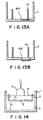
- the position and shape of coupling tube 16 can be freely determined, and coupling tube 16A formed in the bottom portion of crucible 11 shown in Fig. 13A and coupling tube 16B formed outside the bottom portion of crucible 11 shown in Fig. 13B can be used.
- the material of crucible 11, separation wall 14 or coupling tube 16 can be heat resistant material such as PBN (Pyrolytic Boron Nitride), Si3N4, or SiC other than quartz, or can be quartz coated with PBN, Si3N4, or SiC.
- r/R is selected to set k eff to be equal to or near 1.
- a practically effective crystal pulling method using an integral type double crucible in which the condition that b > L ⁇ 4a and 30 mm > a > 2 mm for coupling tube 16 used in the integral type double crucible method, and ⁇ T > 15°C, are set for pulling a Si single crystal.
- doped melt ML1 and undoped melt ML2 are respectively received in inner chamber 20 and outer chamber 21, and are communicated by means of a coupling tube which satisfies the condition b > L ⁇ 4a.
- k eff may be set equal to or near 1.
- the yield relating to the resistivity of pulling crystal can be enhanced to approx. 100%, or the yield can be significantly enhanced in comparison with the prior art case by controlling the resistivity and other characteristics.
Landscapes
- Chemical & Material Sciences (AREA)
- Engineering & Computer Science (AREA)
- Crystallography & Structural Chemistry (AREA)
- Materials Engineering (AREA)
- Metallurgy (AREA)
- Organic Chemistry (AREA)
- Crystals, And After-Treatments Of Crystals (AREA)
- Liquid Deposition Of Substances Of Which Semiconductor Devices Are Composed (AREA)
Claims (13)
- Kristallziehvorrichtung, umfassend:
einen einen vorbestimmten Innenwandradius R aufweisenden äußeren Ziehtiegel (11) zum Aufnehmen einer ersten Materialschmelze (ML2),
einen koaxial im äußeren Ziehtiegel (11) angeordneten inneren Ziehtiegel (14, 24) zum Aufnehmen einer zweiten Materialschmelze (ML1), wobei der innere Ziehtiegel (14, 24) eine Innenumfangslänge b (= 2πr) und einen Radius r im wesentlichen gleich dem √k-fachen des Radius R aufweist, wobei k für den Verteilungskoeffizienten eines Dotierstoffs steht, der im Betrieb in der zweiten Materialschmelze (ML1) enthalten ist,
ein Verbindungsmittel (16) einer vorbestimmten Länge L und eines vorbestimmten Innendurchmessers a, um es der ersten Materialschmelze (ML2) zu ermöglichen, in einer Richtung aus dem äußeren Ziehtiegel (11) zum inneren Ziehtiegel (14, 24) zu fließen, wobei b > L ≧ 4a gilt, und
eine Einrichtung (EM) zum Anlegen eines vertikalen Magnetfelds einer vorgeschriebenen Stärke von mehr als 0,15 T (1500 Gauß) an die zweite Materialschmelze (ML1) zwecks Unterdrückung von Konvektion und damit Unterdrückung des Ausfließens von in der zweiten Materialschmelze (ML1) enthaltenem Fremdatom (Dotierstoff). - Vorrichtung nach Anspruch 1, dadurch gekennzeichnet, daß das Verbindungsmittel (16) eine in der Außenwand (14) an der Unterseite des inneren Ziehtiegels (14, 24) geformte Bohrung (15) und ein eine Effektivlänge L aufweisendes und mit der Bohrung (15) versehenes Rohr (16) umfaßt und die im äußeren Ziehtiegel (11) enthaltene erste Materialschmelze (ML2) über das Rohr (16) und die Bohrung (15) in den innerne Ziehtiegel (14, 24) fließen kann.
- Vorrichtung nach Anspruch 1, dadurch gekennzeichnet, daß der innere Ziehtiegel (14, 24) Positioniermittel (24a, 24c, 24d) zum Positionieren des inneren Ziehtiegels (14, 24) koaxial zu einer Innenseite des äußeren Ziehtiegels (11) aufweist und der innere Ziehtiegel (14, 24) herausnehmbar am äußeren Ziehtiegel (11) montierbar bzw. in diesen einsetzbar ist.
- Vorrichtung nach Anspruch 1, dadurch gekennzeichnet, daß das Verbindungsmittel (16) eine in der Außenwand (14) an der Unterseite des inneren Ziehtiegels (14, 24) geformte Bohrung (15) und ein die Effektivlänge L und einen Innendurchmesser a aufweisendes und mit der Bohrung (15) versehenes Rohr (16) umfaßt und der innere Ziehtiegel (14, 24) eine Trennwand (14) zum Trennen der vom inneren Ziehtiegel (14, 24) aufgenommenen zweiten Materialschmelze (ML1) von der ersten Materialschmelze (ML2) aufweist.
- Vorrichtung nach Anspruch 4, dadurch gekennzeichnet, daß der Innendurchmesser a des Rohrs (16) wesentlich kleiner als 30 mm und größer als 2 mm ist.
- Vorrichtung nach Anspruch 1, dadurch gekennzeichnet, daß die Magnet(feld)anlegeeinrichtung (EM) zum Anlegen von mehr als einem vorbestimmten Magnetfeld (1500 Gauß) in einer vorgegebenen Richtung in bezug auf die zweite Materialschmelze (ML1) an der Außenseite des äußeren Ziehtiegels (11) vorgesehen ist.
- Vorrichtung nach einem der Ansprüche 1 bis 6, dadurch gekennzeichnet, daß der Werkstoff von innerem und äußerem Ziehtiegel (14, 24 bzw. 11) aus Quarz, pyrolytischem Bornitrid, Si₃N₄ oder SiC besteht.
- Vorrichtung nach einem der Ansprüche 1 bis 7, dadurch gekennzeichnet, daß die vorgeschriebene Stärke des Magnetfelds 0,3 T (3000 Gauß) beträgt.
- Kristallziehverfahren zum Ziehen eines Halbleiterkristalls (17) aus einer in einer inneren Kammer (20) befindlichen Materialschmelze (ML1), während von einer äußeren Kammer (21) aufgenommene Materialschmelze (ML2) der inneren Kammer (20) über ein zwischen innerer und äußerer Kammer (20 bzw. 21), die durch eine koaxial im Ziehtiegel (11) angeordnete zylindrische Trennwand (14) in einen Halbleiterkristall-Ziehtiegel (11) unterteilt sind, vorgesehenes Verbindungsrohr (16) zugeführt wird, dadurch gekennzeichnet, daß die Länge L des Verbindungsrohrs eingestellt wird, um der Bedingung oder Beziehung b > L ≧ 4a zu genügen, wenn der Innendurchmesser des Verbindungsrohrs gleich a ist und die durch den inneren Ziehtiegel (14, 24) gebildete innere Kammer eine Innenumfangslänge b (= 2πr) und einen Radius im wesentlichen gleich dem √k-fachen des Radius R aufweist, wobei k den Verteilungskoeffizienten eines Dotierstoffs, der im Betrieb in der zweiten Materialschmelze (ML1) enthalten ist, bedeutet, und ein vertikales Magnetfeld mit einer vorgeschriebenen Stärke von mehr als 0,15 T (1500 Gauß) an die zweite Materialschmelze (ML1) angelegt wird, um Konvektion und damit das Ausfließen von in der zweiten Materialschmelze (ML1) enthaltenem Fremdatom (Dotierstoff) zu unterdrücken.
- Kristallziehverfahren nach Anspruch 8, dadurch gekennzeichnet, daß die ersten und zweiten Materialschmelzen (ML2 bzw. ML1) Siliziumschmelzen sind.
- Kristallziehverfahren nach Anspruch 10, dadurch gekennzeichnet, daß die Temperatur der ersten Materialschmelze (ML2) in der Nähe der Trennwand (14) um im wesentlichen mindestens 15°C höher gehalten wird als die der zweiten Materialschmelze (ML1) in der Nähe der Trennwand (14).
- Kristallziehverfahren nach Anspruch 10, dadurch gekennzeichnet, daß der äußere Ziehtiegel (11) erwärmt wird, um die Temperatur der ersten Materialschmelze (ML2) in der Nähe der Trennwand (14) um im wesentlichen mindestens 30°C höher als die der zweiten Materialschmelze (ML1) in der Nähe der Trennwand (14) zu halten.
- Kristallziehverfahren nach Anspruch 10, dadurch gekennzeichnet, daß die vorgeschriebene Stärke des Magnetfelds 0,3 T (3000 Gauß) beträgt.
Applications Claiming Priority (2)
| Application Number | Priority Date | Filing Date | Title |
|---|---|---|---|
| JP63039152A JP2755588B2 (ja) | 1988-02-22 | 1988-02-22 | 結晶引上げ方法 |
| JP39152/88 | 1988-02-22 |
Publications (2)
| Publication Number | Publication Date |
|---|---|
| EP0330141A1 EP0330141A1 (de) | 1989-08-30 |
| EP0330141B1 true EP0330141B1 (de) | 1993-08-18 |
Family
ID=12545135
Family Applications (1)
| Application Number | Title | Priority Date | Filing Date |
|---|---|---|---|
| EP89102992A Expired - Lifetime EP0330141B1 (de) | 1988-02-22 | 1989-02-21 | Vorrichtung und Verfahren zum Kristallziehen |
Country Status (5)
| Country | Link |
|---|---|
| US (1) | US5021225A (de) |
| EP (1) | EP0330141B1 (de) |
| JP (1) | JP2755588B2 (de) |
| KR (1) | KR920009563B1 (de) |
| DE (1) | DE68908435T2 (de) |
Families Citing this family (17)
| Publication number | Priority date | Publication date | Assignee | Title |
|---|---|---|---|---|
| JP2585123B2 (ja) * | 1990-04-13 | 1997-02-26 | 東芝セラミックス株式会社 | シリコン単結晶の製造方法 |
| JP3015656B2 (ja) * | 1994-03-23 | 2000-03-06 | 株式会社東芝 | 半絶縁性GaAs単結晶の製造方法および製造装置 |
| JP3769800B2 (ja) * | 1996-01-12 | 2006-04-26 | 株式会社Sumco | 単結晶引上装置 |
| JPH09194289A (ja) * | 1996-01-12 | 1997-07-29 | Mitsubishi Materials Shilicon Corp | 単結晶引上装置 |
| US6179914B1 (en) * | 1999-02-02 | 2001-01-30 | Seh America, Inc. | Dopant delivery system and method |
| TW499696B (en) * | 1999-04-27 | 2002-08-21 | Tokyo Electron Ltd | Processing apparatus and processing method |
| KR100702538B1 (ko) * | 2005-02-28 | 2007-04-04 | 네오세미테크 주식회사 | 액상봉입형 초크랄스키법에 의한 갈륨비소 단결정 성장용반응용기 인상 장치 |
| MY159737A (en) | 2010-09-03 | 2017-01-31 | Gtat Ip Holding Llc | Silicon single crystal doped with gallium, indium, or aluminum |
| KR20140097971A (ko) * | 2011-04-14 | 2014-08-07 | 지티 어드밴스드 씨제트 엘엘씨 | 균등한 다중 도판트들을 갖는 실리콘 잉곳 및 그 제조방법과 제조장치 |
| US10544517B2 (en) * | 2011-05-06 | 2020-01-28 | Gtat Ip Holding Llc. | Growth of a uniformly doped silicon ingot by doping only the initial charge |
| US20140144371A1 (en) * | 2012-11-29 | 2014-05-29 | Solaicx, Inc. | Heat Shield For Improved Continuous Czochralski Process |
| US20140261155A1 (en) * | 2013-03-15 | 2014-09-18 | Memc Electronic Materials, Inc. | Crucible for controlling oxygen and related methods |
| US9863062B2 (en) | 2013-03-14 | 2018-01-09 | Corner Star Limited | Czochralski crucible for controlling oxygen and related methods |
| US9822466B2 (en) | 2013-11-22 | 2017-11-21 | Corner Star Limited | Crystal growing systems and crucibles for enhancing heat transfer to a melt |
| KR101680213B1 (ko) * | 2015-04-06 | 2016-11-28 | 주식회사 엘지실트론 | 실리콘 단결정 잉곳의 성장 방법 |
| WO2016179022A1 (en) * | 2015-05-01 | 2016-11-10 | Sunedison, Inc. | Methods for producing single crystal ingots doped with volatile dopants |
| US10407797B2 (en) * | 2017-05-04 | 2019-09-10 | Corner Start Limited | Crystal pulling system and method including crucible and barrier |
Family Cites Families (17)
| Publication number | Priority date | Publication date | Assignee | Title |
|---|---|---|---|---|
| FR66315E (fr) * | 1906-09-03 | 1956-06-29 | Int Standard Electric Corp | Dispositifs amplificateurs utilisant des semi-conducteurs ou des cristaux |
| US2809136A (en) * | 1954-03-10 | 1957-10-08 | Sylvania Electric Prod | Apparatus and method of preparing crystals of silicon germanium group |
| NL121446C (de) * | 1958-11-17 | |||
| NL6917398A (de) * | 1969-03-18 | 1970-09-22 | ||
| DE2152801A1 (de) * | 1970-11-09 | 1972-05-10 | Little Inc A | Verfahren und Ofen zum Ziehen von Kristallen gleichförmiger Zusammensetzung nach dem Czochralski-Verfahren |
| US4036595A (en) * | 1975-11-06 | 1977-07-19 | Siltec Corporation | Continuous crystal growing furnace |
| US4190631A (en) * | 1978-09-21 | 1980-02-26 | Western Electric Company, Incorporated | Double crucible crystal growing apparatus |
| JPS5556098A (en) * | 1978-10-17 | 1980-04-24 | Chiyou Lsi Gijutsu Kenkyu Kumiai | Method and apparatus for producing si single crystal rod |
| US4353875A (en) * | 1978-11-06 | 1982-10-12 | Allied Corporation | Apparatus for growing crystalline materials |
| US4456499A (en) * | 1979-05-25 | 1984-06-26 | At&T Technologies, Inc. | Double crucible Czochralski crystal growth method |
| US4246064A (en) * | 1979-07-02 | 1981-01-20 | Western Electric Company, Inc. | Double crucible crystal growing process |
| US4659421A (en) * | 1981-10-02 | 1987-04-21 | Energy Materials Corporation | System for growth of single crystal materials with extreme uniformity in their structural and electrical properties |
| JPS58172290A (ja) * | 1982-03-31 | 1983-10-11 | Sumitomo Electric Ind Ltd | 化合物半導体単結晶の引上方法および装置 |
| JPS5913693A (ja) * | 1982-07-15 | 1984-01-24 | Toshiba Corp | 化合物半導体単結晶育成装置 |
| DE3316547C2 (de) * | 1983-05-06 | 1985-05-30 | Philips Patentverwaltung Gmbh, 2000 Hamburg | Kalter Tiegel für das Erschmelzen nichtmetallischer anorganischer Verbindungen |
| JPS6033294A (ja) * | 1983-07-29 | 1985-02-20 | Toshiba Ceramics Co Ltd | 単結晶半導体引上装置 |
| JPS6379790A (ja) * | 1986-09-22 | 1988-04-09 | Toshiba Corp | 結晶引上げ装置 |
-
1988
- 1988-02-22 JP JP63039152A patent/JP2755588B2/ja not_active Expired - Lifetime
-
1989
- 1989-02-21 EP EP89102992A patent/EP0330141B1/de not_active Expired - Lifetime
- 1989-02-21 US US07/312,847 patent/US5021225A/en not_active Expired - Lifetime
- 1989-02-21 DE DE89102992T patent/DE68908435T2/de not_active Expired - Fee Related
- 1989-02-22 KR KR1019890002086A patent/KR920009563B1/ko not_active Expired
Also Published As
| Publication number | Publication date |
|---|---|
| US5021225A (en) | 1991-06-04 |
| DE68908435T2 (de) | 1994-01-05 |
| KR890013228A (ko) | 1989-09-22 |
| JP2755588B2 (ja) | 1998-05-20 |
| KR920009563B1 (ko) | 1992-10-19 |
| EP0330141A1 (de) | 1989-08-30 |
| DE68908435D1 (de) | 1993-09-23 |
| JPH01215788A (ja) | 1989-08-29 |
Similar Documents
| Publication | Publication Date | Title |
|---|---|---|
| EP0330141B1 (de) | Vorrichtung und Verfahren zum Kristallziehen | |
| EP2705178B1 (de) | Wachstum eines gleichmässig dotierten siliciumstabs durch alleinige dotierung nur der anfänglichen ladung | |
| US4659421A (en) | System for growth of single crystal materials with extreme uniformity in their structural and electrical properties | |
| EP0140509B1 (de) | LEC-Verfahren und Vorrichtung zur Züchtung eines Einkristalls von Halbleiterverbindung | |
| US4894206A (en) | Crystal pulling apparatus | |
| US12227877B2 (en) | Continuous replenishment crystal growth | |
| US4936949A (en) | Czochraski process for growing crystals using double wall crucible | |
| US11767610B2 (en) | Use of buffer members during growth of single crystal silicon ingots | |
| EP0141495B1 (de) | Verfahren zur Züchtung eines Einkristalls | |
| JPH01192789A (ja) | 結晶引上げ装置及び結晶引上げ方法 | |
| EP0219966B1 (de) | Verfahren für Kristallzüchtung | |
| US5143704A (en) | Apparatus for manufacturing silicon single crystals | |
| EP0330189B1 (de) | Verfahren zur Ziehung eines Halbleiter-Kristalls | |
| US4334948A (en) | Method of and apparatus for growing crystal ribbon | |
| EP0141649B1 (de) | Vorrichtung zur Züchtung eines Einkristalls | |
| EP4352283B1 (de) | Verwendung von quarzplatten beim wachsen von siliziumeinkristallblöcken | |
| JP2023539379A (ja) | シリコン充填物を覆うためのカバー部材を有する結晶引上げシステム、及びシリコン溶融物をるつぼアセンブリ内で成長させるための方法 | |
| EP0206514B1 (de) | Doppeltiegel zum Ziehen von Einkristallen | |
| JPH02160688A (ja) | シリコン単結晶の製造方法及び装置 |
Legal Events
| Date | Code | Title | Description |
|---|---|---|---|
| PUAI | Public reference made under article 153(3) epc to a published international application that has entered the european phase |
Free format text: ORIGINAL CODE: 0009012 |
|
| 17P | Request for examination filed |
Effective date: 19890317 |
|
| AK | Designated contracting states |
Kind code of ref document: A1 Designated state(s): DE FR GB |
|
| RIN1 | Information on inventor provided before grant (corrected) |
Inventor name: KOJIMA, MASAKATU C/O PATENT DIVISION Inventor name: YAMASHITA, YOUJI C/O PATENT DIVISION |
|
| 17Q | First examination report despatched |
Effective date: 19910702 |
|
| GRAA | (expected) grant |
Free format text: ORIGINAL CODE: 0009210 |
|
| AK | Designated contracting states |
Kind code of ref document: B1 Designated state(s): DE FR GB |
|
| REF | Corresponds to: |
Ref document number: 68908435 Country of ref document: DE Date of ref document: 19930923 |
|
| ET | Fr: translation filed | ||
| PLBE | No opposition filed within time limit |
Free format text: ORIGINAL CODE: 0009261 |
|
| STAA | Information on the status of an ep patent application or granted ep patent |
Free format text: STATUS: NO OPPOSITION FILED WITHIN TIME LIMIT |
|
| 26N | No opposition filed | ||
| PGFP | Annual fee paid to national office [announced via postgrant information from national office to epo] |
Ref country code: FR Payment date: 19970211 Year of fee payment: 9 |
|
| PGFP | Annual fee paid to national office [announced via postgrant information from national office to epo] |
Ref country code: GB Payment date: 19970212 Year of fee payment: 9 |
|
| PGFP | Annual fee paid to national office [announced via postgrant information from national office to epo] |
Ref country code: DE Payment date: 19970228 Year of fee payment: 9 |
|
| PG25 | Lapsed in a contracting state [announced via postgrant information from national office to epo] |
Ref country code: GB Free format text: LAPSE BECAUSE OF NON-PAYMENT OF DUE FEES Effective date: 19980221 |
|
| PG25 | Lapsed in a contracting state [announced via postgrant information from national office to epo] |
Ref country code: FR Free format text: THE PATENT HAS BEEN ANNULLED BY A DECISION OF A NATIONAL AUTHORITY Effective date: 19980228 |
|
| GBPC | Gb: european patent ceased through non-payment of renewal fee |
Effective date: 19980221 |
|
| PG25 | Lapsed in a contracting state [announced via postgrant information from national office to epo] |
Ref country code: DE Free format text: LAPSE BECAUSE OF NON-PAYMENT OF DUE FEES Effective date: 19981103 |
|
| REG | Reference to a national code |
Ref country code: FR Ref legal event code: ST |