EP0330189B1 - Verfahren zur Ziehung eines Halbleiter-Kristalls - Google Patents
Verfahren zur Ziehung eines Halbleiter-Kristalls Download PDFInfo
- Publication number
- EP0330189B1 EP0330189B1 EP89103115A EP89103115A EP0330189B1 EP 0330189 B1 EP0330189 B1 EP 0330189B1 EP 89103115 A EP89103115 A EP 89103115A EP 89103115 A EP89103115 A EP 89103115A EP 0330189 B1 EP0330189 B1 EP 0330189B1
- Authority
- EP
- European Patent Office
- Prior art keywords
- crystal
- impurity
- melt
- resistivity
- crucible
- Prior art date
- Legal status (The legal status is an assumption and is not a legal conclusion. Google has not performed a legal analysis and makes no representation as to the accuracy of the status listed.)
- Expired - Lifetime
Links
Images


Classifications
-
- C—CHEMISTRY; METALLURGY
- C30—CRYSTAL GROWTH
- C30B—SINGLE-CRYSTAL GROWTH; UNIDIRECTIONAL SOLIDIFICATION OF EUTECTIC MATERIAL OR UNIDIRECTIONAL DEMIXING OF EUTECTOID MATERIAL; REFINING BY ZONE-MELTING OF MATERIAL; PRODUCTION OF A HOMOGENEOUS POLYCRYSTALLINE MATERIAL WITH DEFINED STRUCTURE; SINGLE CRYSTALS OR HOMOGENEOUS POLYCRYSTALLINE MATERIAL WITH DEFINED STRUCTURE; AFTER-TREATMENT OF SINGLE CRYSTALS OR A HOMOGENEOUS POLYCRYSTALLINE MATERIAL WITH DEFINED STRUCTURE; APPARATUS THEREFOR
- C30B15/00—Single-crystal growth by pulling from a melt, e.g. Czochralski method
- C30B15/02—Single-crystal growth by pulling from a melt, e.g. Czochralski method adding crystallising materials or reactants forming it in situ to the melt
- C30B15/04—Single-crystal growth by pulling from a melt, e.g. Czochralski method adding crystallising materials or reactants forming it in situ to the melt adding doping materials, e.g. for n-p-junction
-
- C—CHEMISTRY; METALLURGY
- C30—CRYSTAL GROWTH
- C30B—SINGLE-CRYSTAL GROWTH; UNIDIRECTIONAL SOLIDIFICATION OF EUTECTIC MATERIAL OR UNIDIRECTIONAL DEMIXING OF EUTECTOID MATERIAL; REFINING BY ZONE-MELTING OF MATERIAL; PRODUCTION OF A HOMOGENEOUS POLYCRYSTALLINE MATERIAL WITH DEFINED STRUCTURE; SINGLE CRYSTALS OR HOMOGENEOUS POLYCRYSTALLINE MATERIAL WITH DEFINED STRUCTURE; AFTER-TREATMENT OF SINGLE CRYSTALS OR A HOMOGENEOUS POLYCRYSTALLINE MATERIAL WITH DEFINED STRUCTURE; APPARATUS THEREFOR
- C30B15/00—Single-crystal growth by pulling from a melt, e.g. Czochralski method
- C30B15/10—Crucibles or containers for supporting the melt
- C30B15/12—Double crucible methods
-
- H—ELECTRICITY
- H10—SEMICONDUCTOR DEVICES; ELECTRIC SOLID-STATE DEVICES NOT OTHERWISE PROVIDED FOR
- H10P—GENERIC PROCESSES OR APPARATUS FOR THE MANUFACTURE OR TREATMENT OF DEVICES COVERED BY CLASS H10
- H10P14/00—Formation of materials, e.g. in the shape of layers or pillars
- H10P14/20—Formation of materials, e.g. in the shape of layers or pillars of semiconductor materials
-
- Y—GENERAL TAGGING OF NEW TECHNOLOGICAL DEVELOPMENTS; GENERAL TAGGING OF CROSS-SECTIONAL TECHNOLOGIES SPANNING OVER SEVERAL SECTIONS OF THE IPC; TECHNICAL SUBJECTS COVERED BY FORMER USPC CROSS-REFERENCE ART COLLECTIONS [XRACs] AND DIGESTS
- Y10—TECHNICAL SUBJECTS COVERED BY FORMER USPC
- Y10S—TECHNICAL SUBJECTS COVERED BY FORMER USPC CROSS-REFERENCE ART COLLECTIONS [XRACs] AND DIGESTS
- Y10S117/00—Single-crystal, oriented-crystal, and epitaxy growth processes; non-coating apparatus therefor
- Y10S117/90—Apparatus characterized by composition or treatment thereof, e.g. surface finish, surface coating
Definitions
- This invention relates to a crystal pulling method for growing semiconductor crystal using a crucible called an integral type double crucible, and more particularly to a uniform resistivity control method used in a case where two kinds of dopants or two different dopant concentration melts are used.
- impurity concentration distribution C in the longitudinal direction of the grown single crystal can be expressed as follows.
- C kCo(l-G) k-1
- k a segregation coefficient of dopant
- Co the initial impurity concentration of the melt
- G solidification ratio
- inner crucible 2 is arranged as a floating crucible inside outer crucible 1, and small hole 3 is formed in the bottom portion of inner crucible 2.
- the balance between the buoyancy and gravitational force of the inner crucible is utilized, for example, or the outer crucible is lifted relative to the fixed inner crucible, so that melt 5 can be supplied from the outer crucible to the inner crucible, thus keeping the height h of the surface level of the melt in the inner crucible at a constant level.
- the impurity concentration of melt 5 in the outer crucible is Co
- the impurity concentration of melt 4 in the inner crucible is Co/k (k is a segregation coefficient).
- the concentration of impurity taken into pulling crystal 6 becomes Co in the pulling process in which surface level h of the melt is kept constant.
- melt pure silicon or germanium
- impurity concentration of pulling crystal 6 can also be kept at constant value Co.
- the melt is consumed.
- the melt surface level in the inner crucible cannot be kept constant, and the impurity concentration of crystal 6 will vary (increase) as the solidification ratio increases. That is, the impurity concentration can be kept constant only within the following range of the solidification ratio X: O ⁇ X ⁇ 1-(h/H) where H is the initial surface level of the melt in the outer crucible, and h is the surface level of the melt in the inner crucible to be kept constant during the pulling process.
- the resistivity can be kept constant only when the solidification ratio is less than 0.6 to 0.7. If the solidification ratio becomes larger, the resistivity will significantly vary.
- the inventors of this invention have proposed a pulling apparatus having an integral type double crucible (Japanese Patent Application No. 61-221896.
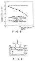
- the pulling apparatus is shown in Fig. 1.
- 11 denotes an outer crucible
- 14 denotes a cylindrical separation wall integrally and coaxially formed with outer crucible 11.
- the inner space of outer crucible 11 is divided into inner chamber 20 and outer chamber 21 by separation wall 14.
- Inner chamber 20 and outer chamber 21 are connected with each other by means of small hole 15 and narrow pipe-like coupling tube 16 formed with small hole 15.
- melt ML2 in outer chamber 21 is supplied to inner chamber 20 while single crystal 17 is being pulled from melt ML1 in the inner chamber.
- the impurity of melt ML1 in the inner chamber is inhibited from flowing into the outer chamber by the preset length L of coupling tube 16 not only during the pulling process but also when melt is not transferred from outer chamber 21 to inner chamber 20.
- Length L is determined to be larger than four times inner diameter a of tube 16.
- the integral type double crucible is different from the floating type double crucible which has only hole 15.
- One of the proposed crystal pulling methods using the integral type double crucible is to solve the problem that the impurity concentration in the longitudinal direction of crystal formed by the floating type double crucible method is limited by the solidification ratio used in equation (1).
- doped material melt ML1 impurity concentration Ci
- undoped material melt ML2 is received in outer chamber 21.
- ratio r/R of radius r of inner chamber 20 and radius R of outer chamber 21 is set to be equal to square root k of segregation coefficient k of the doping impurity and crystal 17 of impurity concentration kCi is pulled by ⁇ R 2 ⁇ H ( ⁇ H is decrease in the surface level of melt ML1) from melt ML1 in the inner chamber.
- the impurity concentration in the longitudinal direction of crystal 17 can be kept at constant value kCi.
- electrically conductive impurity (B, Al or the like) flows out of the crucible itself and may cause an inadvertent influence, making it difficult to attain crystal of high and constant resistivity.
- electrically conductive impurity B, Al or the like
- An object of this invention is to provide a novel crystal pulling method by which substantially 100% of yield with respect to the resistivity of crystal can be attained.
- an object of this invention is to provide a crystal pulling method capable of controlling the resistivity in the longitudinal direction of crystal (1) when electrically conductive impurity of the opposite or the same conductivity type is unintentionally introduced into the melt, (2) when two kinds of electrically conductive impurity of the opposite conductivity types are intentionally introduced into the melt, or (3) when melt regions with two different impurity concentration levels of the same conductivity type are intentionally formed.
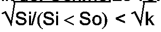
- a crystal pulling method which comprises the steps of: coaxially disposing a separation wall 14 in a semiconductor crystal pulling crucible to divide said crucible into an inner chamber 20 and an outer chamber 21; putting first doped material melt ML1 into said inner chamber 20 and second material melt ML2 into said outer chamber 21; and pulling crystal from the first material melt ML1 in said inner chamber 20 while the second material melt ML2 in said outer chamber 21 is being supplied to said inner chamber 20 via coupling means 15, 16 for connecting said inner chamber 20 and outer chamber 21 with each other and suppressing an outflow of impurity from said inner chamber 20 to said outer chamber 21, and which is characterized in that the second material melt ML2 in said outer chamber 21 is undoped melt; and the condition of Si/(Si+So) > k is set to increase the doping impurity concentration in the longitudinal direction of the crystal so as to compensate for the influence of the opposite type conductive impurity which has flowed out of the crucible and mixed into the melt, or the condition
- a crystal pulling method which comprises the steps of: coaxially disposing a tubular separation wall 14 in a cylindrical semiconductor crystal pulling crucible 11 to divide said crucible 11 into an inner chamber 20 and an outer chamber 21 said tubular separation wall 14 having a diameter (2r) smaller than a diameter (2R) of said crucible 11, putting first doped material melt ML1 into said inner chamber 20 and second material melt ML2 into said outer chamber 21; and pulling crystal from the first material melt ML1 in said inner chamber 20 while the second material melt ML2 in said outer chamber 21 is being supplied to said inner chamber 20 via coupling means 15, 16 for connecting said inner chamber 20 and outer chamber 21 with each other and suppressing an outflow of impurity from said inner chamber 20 to said outer chamber 21, and which is characterized in that the second material melt ML2 in said outer chamber 21 is undoped melt; and the condition of (r/R) > /k is set to increase the doping impurity concentration in the longitudinal direction of the crystal so as to compensate for
- the crystal pulling method of this invention for compensating for variation in the characteristic of the pulling crystal due to inadvertent introduction of electrically conductive impurity is effected by using an integral type double crucible.
- This crucible is divided into inner chamber 20 and outer chamber 21 by concentric or coaxial cylindrical separation wall 14.
- first doped material melt ML1 is received in inner chamber 20
- second undoped material melt ML2 is received in outer chamber 21.
- (r/R) is set to be larger than k so as to increase the concentration of the doping impurity in the longitudinal direction of the crystal, thus compensating for the influence by impurity of the opposite conductivity types unintentionally introduced into crystal 17.
- (r/R) is set to be smaller than k so as to decrease the concentration of the doping impurity in the longitudinal direction of the crystal, thus compensating for the influence by impurity of the same conductivity types unintentionally introduced into crystal 17.
- the influence of changing the resistivity in the longitudinal direction of the crystal by P-type or N-type impurity unintentionally introduced into N-type crystal can be compensated for by intentionally changing the concentration of the N-type doping impurity in the longitudinal direction of the crystal.
- the resistivity in the longitudinal direction of the pulling crystal can be controlled.
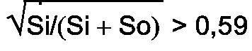
- the resistivity of more than 20 ⁇ cm is controlled in the longitudinal direction of phosphorus (P) doped N-type high resistance silicon single crystal pulled from a quartz crucible from which acceptor, such as B or Al, flows out of the quartz crucible, and segregation coefficient k is set at 0.35 and therefore k is 0.59.
- the ratio of (r/R) is set to satisfy the condition of 0.85 ⁇ (r/R) > 0.59. Selection of the resistivity in the above range can be made by previously detecting the amount of acceptor flowing out of the crucible.
- ratio r/R must be understood as ratio Si/(So+Si) when the upper surface area of melt in inner chamber 20 is Si and the upper surface area of melt in outer chamber 21 is So. That is, the above range is determined by using Si/(Si+So) instead of r/R when the crucible and separation wall are not cylindrical. The range must be set to satisfy the condition that 0.85 > Si/(Si+So) > 0.59, for example.
- first doped material melt ML1 is received in inner chamber 20 of the integral type double crucible, and conductive impurity having a conductivity type (P) opposite to the conductivity type (N) of the doped impurity of melt ML1 is introduced into second material melt ML2 in outer chamber 21.
- the doped impurity concentration of melt ML1 which will become high during the pulling process, is reduced and compensated for by introducing melt ML2 into the inner chamber.
- the resistivity variation in the longitudinal direction of pulling crystal can thus be controlled.
- concentration C A S (x) of impurity A which has been doped into melt ML1 in the inner chamber and has been taken into pulling crystal 17 can be expressed as follows.
- k eff A k A x ( ⁇ R 2 / ⁇ r 2 ) and k A is the segregation coefficient of impurity A and C A m (0) is the concentration of impurity A in melt of the inner chamber at the initial pulling stage.
- concentration C B S (x) of impurity B which has been doped into melt ML2 in the outer chamber and taken into pulling crystal 17 can be expressed as follows.
- k eff B k B x ( ⁇ R 2 / ⁇ r 2 ) and k B is the segregation coefficient of impurity B and C B m (0) is the concentration of impurity B in melt of the outer chamber at the initial pulling stage.
- the effective concentration of impurity A in the crystal with solidification ratio x can be kept at substantially the same value as that of the crystal obtained at the initial pulling stage by such a manner that one of impurity A and impurity B compensates for the other thereof.
- concentration C B m (0) of impurity B which determines C B S (x) in equation (4) is so adjusted to substantially satisfy the following equation.
- C S A (x) - C S A (0) C S B (x)
- the resistivity becomes equal in portions with solidification ratios of 0 and x (0 ⁇ x ⁇ 0.85). Further, the resistivity in portions with the segregation coefficient other than the portion of x in the solidification ratio can be controlled, so that deviation of the resistivity from a desired value can be suppressed within a relatively narrow range.
- impurity concentration Cs(x) in the pulling crystal can be expressed as follows.
- k eff k x ( ⁇ R 2 / ⁇ r 2 ) and k is the segregation coefficient of impurity
- Ci(0) is the impurity concentration of the melt in the inner chamber at the initial pulling stage
- Co(0) is the impurity concentration of the melt in the outer chamber at the initial pulling stage.
- the impurity concentration in the crystal can be made constant in the longitudinal direction thereof.
- a coupling mechanism (15, 16) provided between the inner and outer chambers is used to suppress the outflow of doped impurity included in melt ML1 in the inner chamber of the integral type double crucible to outer chamber 21.
- the coupling mechanism is not limited to pipe-like tube 16.
- Fig. 1 shows a crystal pulling apparatus used in one embodiment of this invention.
- graphite crucible 12 is mounted on vertically movable and rotatable crucible shaft 13, and quartz crucible 11 of 30,5cm (12 ⁇ ) ⁇ is disposed in close contact with the inner surface of graphite crucible 12.
- Quartz cylindrical separation wall 14 with radius r is coaxially disposed in and bonded to crucible 11.
- L is determined to satisfy the condition: 2 ⁇ r > L ⁇ 4a.
- the charge amount of silicon material was 14 kg.
- the coupling means is constructed only by means of small hole 15, supply of dopant impurity to inner chamber 20 or outer chamber 21 is effected after the grown crystal in the stage of the shouldering becomes 10 mm ⁇ and before the straight body thereof, so that reverse flow of the melt from inner chamber 20 to outer chamber 21 is prevented.
- the coupling means between the inner and outer chambers is formed of pipe-like passage 16 which has an effect of suppressing the outflow of impurity from inner chamber melt ML1 to outer chamber melt ML2, supply of dopant impurity is effected after material silicon has melted and the surface levels of the melts in the inner and outer chambers have become equal to each other.
- impurity which is flowed out from the quartz crucible is compensated for and high resistance N-type single crystal having a uniform resistivity of 50 ⁇ cm and 100 ⁇ cm, which is constant in the longitudinal direction thereof, is pulled.
- inner diameter 2r of the separation wall was variously changed, crystals were grown from the undoped melt (in both the inner and outer chambers), and then the conductivity types and the resistances of the grown crystals were detected and the apparent impurity concentration was derived based on these detected values.
- the conductivity type of the flow-out impurity from crucible body 11 and separation wall 14 of quartz was detected to be P-type, and the resistivity in the longitudinal direction was detected to decrease from the head portion of 1000 to 2000 ⁇ cm to the tail portion of several hundreds ⁇ cm.
- Fig. 2 shows the distribution of the derived impurity concentration.
- Ratio r/R was set to 0.70 according to the result of Fig. 2.
- Phosphorus was doped into melt ML1 in the inner chamber so as to set the resistivity of the crystal head portion to 50 ⁇ cm (the concentration of phosphorus is 1 x 10¹⁴ atoms/cc).
- Melt ML2 in the outer chamber was kept undoped. Under this condition, single crystal 17 of N-type high resistance was pulled.
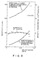
- Fig. 3 shows the distribution of the resistivity and the impurity concentration in the longitudinal direction of single crystal 17.
- Fig. 3 indicates that gradually increasing amount of P-type impurity (mark ⁇ ) flowing out of the quartz crucible (11, 14) with ratio r/R set at 0.70 and unintentionally doped into crystal 17, can be compensated for by gradually increasing concentration (mark o) of N-type impurity (P) intentionally doped into crystal 17 and, consequently, the resistivity (mark ⁇ ) of crystal 17 can be made substantially constant in the longitudinal direction.
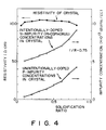
- Fig. 5 shows the distribution of impurity concentration of high resistance silicon single crystal having N-type resistivity of 50 ⁇ cm and pulled by use of the quartz floating type double crucible.
- solidification ratio x is set in the range of 0 ⁇ x ⁇ 1-(h/H)
- the effective impurity concentration (mark o) or the resistivity cannot be made constant.
- N-type impurity: P its segregation coefficient is 0.35
- boron P-type impurity: B, its segregation coefficient is 0.80
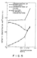
- N-type silicon single crystal 17 with constant resistivity (5 ⁇ cm) in the longitudinal direction was pulled while ratio r/R was variously changed.
- C B m (0) was determined based on equation (11), and the expected resistivity and effective phosphorus concentration in the longitudinal direction of crystal of 5 ⁇ cm were obtained by calculation as shown in table 2.
- the resistivity can be sufficiently expected to be made constant.
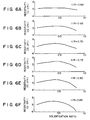
- Figs. 6A to 6F show the results of the verification experiments effected in conditions that ratios r/R were respectively set at 0.60, 0.65, 0.70, 0.75, 0.80, and 0.85; phosphorus and boron were respectively doped into melts in inner chamber 20 and outer chamber 21, and the effective phosphorus concentration of a portion in which solidification ratio x is 0.70 and that of a portion in which solidification ratio x is 0 were controlled to become equal to each other. From the experiments, it was verified that the resistivity was kept substantially constant at a value of 5 ⁇ cm in the longitudinal direction as indicated by the above theory.
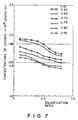
- ratio r/R when ratio r/R is set to any value within the range between 0.60 (or 0.59) and 0.85, the resistivity in the longitudinal direction of crystal can be made constant. Therefore, ratio r/R can be set to a proper value which is preferable to a characteristic other than the resistivity. For example, oxygen concentration [Oi] in silicon single crystal becomes high as the diameter of the crucible with respect to that of the crystal becomes smaller.
- Fig. 7 shows oxygen concentration [Oi] in the longitudinal direction of crystals obtained in the above verification experiments. As is clearly seen from Fig. 7, if the specific range of 1.55 to 1.85 x 10¹⁸ atoms/cc is set with respect to [Oi], the specific [Oi] values can be satisfied by setting ratio r/R to 0.70 or 0.75.
- ratio r/R is set to 0.70
- boron is doped into the melts in the inner and outer chambers
- single crystal with the resistivity of 10 ⁇ cm and oxygen concentration of 1.55 to 1.85 x 10¹⁸ atoms/cc is grown.
- equation (9) is solved as follows.
- Ci(0) is the concentration of boron in the melt in the inner chamber at the initial pulling stage
- Co(0) is the concentration of boron in the melt in the outer chamber at the initial pulling stage.
- Crystal was pulled in a condition that boron was doped into the melt in inner chamber 20 at the concentration of Ci(0) to attain the resistivity of 10 ⁇ cm and boron was doped into the melt in outer chamber 21 at a concentration of Co(0) to satisfy equation (12). Then, the single crystal in which the resistivity was constant as shown in Fig. 8 and the oxygen concentration was set within the same specified range as that shown by marks ⁇ in Fig. 7 was obtained.
- the resistivity of the single crystal obtained by the CZ technique is shown in Fig. 8.
- the segregation coefficient of boron is 0.80 and is close to 1, and is a dopant which causes the lest variation in the resistivity in the longitudinal direction of crystal.
- the resistivity will significantly vary from 10 ⁇ cm to 7 ⁇ cm.
- the resistivity can be kept substantially constant, and moreover the oxygen concentration can be set to a desired value.
- an integral type double crucible different from that used in the conventional CZ technique or floating type double crucible method is used, and the resistivity in the longitudinal direction of the semiconductor single crystal can be made constant.
- (a) it becomes possible to pull crystal with the constant and high resistivity of 50 ⁇ cm or 100 ⁇ cm which cannot be attained by the conventional method and
- (b) it is possible to pull crystal by use of two types of impurities or two kinds of melts which impurity concentration levels are different each other.
- (c) it is possible to control not only the resistivity but also a characteristic such as the oxygen concentration other than the resistivity.
- the features (a), (b), and (c) can be realized with substantially 100% of yield, and therefore the industrial value of the method of this invention is significantly large.
- crucible 11 and/or separation wall 14 can be formed of Pyrolytic Boron Nitride (PBN), Si 3 N 4 , or SiC, or can be formed of quartz coated with PBN, Si 3 N 4 , or SiC.
Landscapes
- Chemical & Material Sciences (AREA)
- Engineering & Computer Science (AREA)
- Crystallography & Structural Chemistry (AREA)
- Materials Engineering (AREA)
- Metallurgy (AREA)
- Organic Chemistry (AREA)
- Crystals, And After-Treatments Of Crystals (AREA)
- Liquid Deposition Of Substances Of Which Semiconductor Devices Are Composed (AREA)
Claims (10)
- Verfahren zum Ziehen eines Kristalls in folgenden Schritten:
koaxiales Anordnen einer Trennwand (14) in einem Halbleiterkristall-Ziehtiegel zwecks Unterteilung desselben in eine Innenkammer (20) und eine Außenkammer (21),
Einbringen einer ersten dotierten Materialschmelze (ML1) in die Innenkammer (20) und einer zweiten Materialschmelze (ML2) in die Außenkammer (21) und
Ziehen eines Kristalls aus der in der Innenkammer (20) befindlichen ersten Materialschmelze (ML1), während die in der Außenkammer (21) befindliche zweite Materialschmelze (ML2) zur Innenkammer (20) über Verbindungsmittel (15, 16) zum Verbinden der Innenkammer (20) und der Außenkammer (21)- miteinander und zum Unterdrücken eines Ausfließens von Fremdatom (Dotierstoff) aus der Innenkammer (20) zur Außenkammer (21) zugeführt wird,
dadurch gekennzeichnet, daß die in der Außenkammer (21) befindliche zweite Materialschmelze (ML2) eine undotierte Schmelze ist und
die Bedingung
- Verfahren zum Ziehen eines Kristalls nach Anspruch 1, dadurch gekennzeichnet, daß der spezifische Widerstand in Längsrichtung eines aus dem Quarztiegel gezogenen phosphordotierten hochohmigen N-Typ-Siliziumeinkristalls mit einem spezifischen Widerstand von wesentlich mehr als 20 Ω·cm unter einer Bedingung von praktisch 0,85 >
- Verfahren zum Ziehen eines Kristalls nach Anspruch 1, dadurch gekennzeichnet, daß der spezifische Widerstand in Längsrichtung eines aus dem Quarztiegel gezogenen phosphordotierten hochohmigen N-Typ-Siliziumeinkristalls mit einem spezifischen Widerstand von wesentlich mehr als 20 Ω·cm unter einer Bedingung von praktisch 0,75 ≧

- Verfahren zum Ziehen eines Kristalls nach Anspruch 1, dadurch gekennzeichnet, daß der spezifische Widerstand in Längsrichtung des gezogenen Kristalls durch Einführen eines Fremdatoms eines dem Leitfähigkeitstyp des Dotierungsfremdatoms entgegengesetzten Leitfähigkeitstyps in die in der Außenkammer (21) befindliche zweite Materialschmelze (ML2) zum Verdünnen und Kompensieren der Konzentration des Dotierungsfremdatoms, das in der ersten Materialschmelze (ML1) enthalten ist und dessen Konzentration während des Kristallziehprozesses hoch wird, gesteuert wird.
- Verfahren zum Ziehen eines Kristalls nach Anspruch 1, dadurch gekennzeichnet, daß der spezifische Widerstand in Längsrichtung des gezogenen Kristalls durch Einführen eines Fremdatoms mit dem gleichen Leitfähigkeitstyp wie dem des Fremdatoms, mit dem die erste Materialschmelze (ML1) dotiert ist, in die in der Außenkammer (21) befindliche zweite Materialschmelze (ML2) zum Einstellen der Konzentration des in der ersten Materialschmelze (ML1) enthaltenen Dotierungsfremdatoms, dessen Konzentration während des Kristallziehprozesses niedrig wird, gesteuert wird.
- Verfahren zum Ziehen eines Kristalls in foglenden Schritten:
koaxiales Anordnen einer rohrförmigen Trennwand (14) in einem zylindrischen Halbleiterkristall-Ziehtiegel (11) zwecks Unterteilung desselben in eine Innenkammer (20) und eine Außenkammer (21), wobei der Durchmesser (2r) der rohrförmigen Trennwand (14) kleiner ist als der Durchmesser (2R) des Tiegels (11),
Einbringen einer ersten dotierten Materialschmelze (ML1) in die Innenkammer (20) und einer zweiten Materialschmelze (ML2) in die Außenkammer (21) und
Ziehen eines Kristalls aus der in der Innenkammer (20) befindlichen ersten Materialschmelze (ML1), während die in der Außenkammer (21) befindliche zweite Materialschmelze (ML2) zur Innenkammer (20) über Verbindungsmittel (15, 16) zum Verbinden der Innenkammer (20) und der Außenkammer (21) miteinander und zum Unterdrücken eines Ausfließens von Fremdatom (Dotierstoff) aus der Innenkammer (20) zur Außenkammer (21) zugeführt wird,
dadurch gekennzeichnet, daß die in der Außenkammer (21) befindliche zweite Materialschmelze (ML2) eine undotierte Schmelze ist und die Bedingung

k = Verteilungskoeffizient des Dotierfremdatoms in der ersten Materialschmelze (ML1), r = halber Innendurchmesser der Innenkammer (20) und R = halber Innendurchmesser der Außenkammer (21). - Verfahren zum Ziehen eines Kristalls nach Anspruch 6, dadurch gekennzeichnet, daß der spezifische Widerstand in Längsrichtung eines aus dem Quarztiegel gezogenen phosphordotierten hochohmigen Siliziumeinkristalls mit einem spezifischen Widerstand von wesentlich mehr als 20 Ω·cm unter einer Bedingung von praktisch 0,85 > (r/R) > 0,59 gesteuert wird.
- Verfahren zum Ziehen eines Kristalls nach Anspruch 6, dadurch gekennzeichnet, daß der spezifische Widerstand in Längsrichtung eines aus dem Quarztiegel gezogenen phosphordotierten hochohmigen Siliziumeinkristalls mit einem spezifischen Widerstand von wesentlich mehr als 20 Ω·cm unter einer Bedingung von praktisch 0,75 ≧ (r/R) ≧ 0,70 gesteuert wird.
- Verfahren zum Ziehen eines Kristalls nach Anspruch 6, dadurch gekennzeichnet, daß der spezifische Widerstand in Längsrichtung des gezogenen Kristalls durch Einführen eines Fremdatoms eines dem Leitfähigkeitstyp des Dotierungsfremdatoms entgegengesetzten Leitfähigkeitstyps in die in der Außenkammer (21) befindliche zweite Materialschmelze (ML2) zum Verdünnen und Kompensieren der Konzentration des Dotierungsfremdatoms, das in der ersten Materialschmelze (ML1) enthalten ist und dessen Konzentration während des Kristallziehprozesses hoch wird, gesteuert wird.
- Verfahren zum Ziehen eines Kristalls nach Anspruch 6, dadurch gekennzeichnet, daß der spezifische Widerstand in Längsrichtung des gezogenen Kristalls durch Einführen eines Fremdatoms mit dem gleichen Leitfähigkeitstyp wie dem des Fremdatoms, mit dem die erste Materialschmelze (ML1) dotiert ist, in die in der Außenkammer (21) befindliche zweite Materialschmelze (ML2) zum Einstellen der Konzentration des in der ersten Materialschmelze (ML1) enthaltenen Dotierungsfremdatoms, dessen Konzentration während des Kristallziehprozesses niedrig wird, gesteuert wird.
Applications Claiming Priority (2)
| Application Number | Priority Date | Filing Date | Title |
|---|---|---|---|
| JP63042583A JPH085740B2 (ja) | 1988-02-25 | 1988-02-25 | 半導体の結晶引上げ方法 |
| JP42583/88 | 1988-02-25 |
Publications (3)
| Publication Number | Publication Date |
|---|---|
| EP0330189A2 EP0330189A2 (de) | 1989-08-30 |
| EP0330189A3 EP0330189A3 (en) | 1989-10-25 |
| EP0330189B1 true EP0330189B1 (de) | 1992-09-30 |
Family
ID=12640091
Family Applications (1)
| Application Number | Title | Priority Date | Filing Date |
|---|---|---|---|
| EP89103115A Expired - Lifetime EP0330189B1 (de) | 1988-02-25 | 1989-02-22 | Verfahren zur Ziehung eines Halbleiter-Kristalls |
Country Status (5)
| Country | Link |
|---|---|
| US (1) | US5073229A (de) |
| EP (1) | EP0330189B1 (de) |
| JP (1) | JPH085740B2 (de) |
| KR (1) | KR920009564B1 (de) |
| DE (1) | DE68903008T2 (de) |
Families Citing this family (12)
| Publication number | Priority date | Publication date | Assignee | Title |
|---|---|---|---|---|
| US5312600A (en) * | 1990-03-20 | 1994-05-17 | Toshiba Ceramics Co. | Silicon single crystal manufacturing apparatus |
| EP0625595B1 (de) * | 1993-03-29 | 2001-09-19 | Research Development Corporation Of Japan | Regulierung der Sauerstoffkonzentration in einem Einkristall, der aus einer ein Gruppe V Element enthaltenden Schmelze gezogenen wird. |
| JP3015656B2 (ja) * | 1994-03-23 | 2000-03-06 | 株式会社東芝 | 半絶縁性GaAs単結晶の製造方法および製造装置 |
| JP3484870B2 (ja) * | 1996-03-27 | 2004-01-06 | 信越半導体株式会社 | 連続チャージ法によるシリコン単結晶の製造方法およびドーパント供給装置 |
| KR100485151B1 (ko) * | 2002-08-26 | 2005-04-22 | 주식회사 실트론 | 실리콘 단결정 성장 장치 |
| NO322246B1 (no) | 2004-12-27 | 2006-09-04 | Elkem Solar As | Fremgangsmate for fremstilling av rettet storknede silisiumingots |
| JP4760729B2 (ja) * | 2006-02-21 | 2011-08-31 | 株式会社Sumco | Igbt用のシリコン単結晶ウェーハ及びigbt用のシリコン単結晶ウェーハの製造方法 |
| FR2940806B1 (fr) * | 2009-01-05 | 2011-04-08 | Commissariat Energie Atomique | Procede de solidification de semi-conducteur avec ajout de charges de semi-conducteur dope au cours de la cristallisation |
| US10544517B2 (en) | 2011-05-06 | 2020-01-28 | Gtat Ip Holding Llc. | Growth of a uniformly doped silicon ingot by doping only the initial charge |
| US9863062B2 (en) | 2013-03-14 | 2018-01-09 | Corner Star Limited | Czochralski crucible for controlling oxygen and related methods |
| US9822466B2 (en) | 2013-11-22 | 2017-11-21 | Corner Star Limited | Crystal growing systems and crucibles for enhancing heat transfer to a melt |
| WO2016179022A1 (en) * | 2015-05-01 | 2016-11-10 | Sunedison, Inc. | Methods for producing single crystal ingots doped with volatile dopants |
Family Cites Families (10)
| Publication number | Priority date | Publication date | Assignee | Title |
|---|---|---|---|---|
| FR66315E (fr) * | 1906-09-03 | 1956-06-29 | Int Standard Electric Corp | Dispositifs amplificateurs utilisant des semi-conducteurs ou des cristaux |
| GB760778A (en) * | 1953-07-23 | 1956-11-07 | Telefunken Gmbh | Improvements in or relating to the manufacture of single crystals |
| US2892739A (en) * | 1954-10-01 | 1959-06-30 | Honeywell Regulator Co | Crystal growing procedure |
| DE2152801A1 (de) * | 1970-11-09 | 1972-05-10 | Little Inc A | Verfahren und Ofen zum Ziehen von Kristallen gleichförmiger Zusammensetzung nach dem Czochralski-Verfahren |
| US4352784A (en) * | 1979-05-25 | 1982-10-05 | Western Electric Company, Inc. | Double crucible Czochralski crystal growth apparatus |
| US4246064A (en) * | 1979-07-02 | 1981-01-20 | Western Electric Company, Inc. | Double crucible crystal growing process |
| JPS6126591A (ja) * | 1984-07-18 | 1986-02-05 | Fujitsu Ltd | 結晶成長方法 |
| JPS6270291A (ja) * | 1985-09-19 | 1987-03-31 | Toshiba Corp | GaAs単結晶の製造方法及び装置 |
| JPS62226890A (ja) * | 1986-03-27 | 1987-10-05 | Komatsu Denshi Kinzoku Kk | 単結晶及びその製造方法 |
| JPS6379790A (ja) * | 1986-09-22 | 1988-04-09 | Toshiba Corp | 結晶引上げ装置 |
-
1988
- 1988-02-25 JP JP63042583A patent/JPH085740B2/ja not_active Expired - Fee Related
-
1989
- 1989-02-22 DE DE8989103115T patent/DE68903008T2/de not_active Expired - Fee Related
- 1989-02-22 EP EP89103115A patent/EP0330189B1/de not_active Expired - Lifetime
- 1989-02-25 KR KR1019890002233A patent/KR920009564B1/ko not_active Expired
-
1990
- 1990-06-29 US US07/545,098 patent/US5073229A/en not_active Expired - Lifetime
Also Published As
| Publication number | Publication date |
|---|---|
| US5073229A (en) | 1991-12-17 |
| EP0330189A3 (en) | 1989-10-25 |
| KR920009564B1 (ko) | 1992-10-19 |
| DE68903008D1 (de) | 1992-11-05 |
| KR890012893A (ko) | 1989-09-20 |
| JPH01215789A (ja) | 1989-08-29 |
| EP0330189A2 (de) | 1989-08-30 |
| DE68903008T2 (de) | 1993-04-22 |
| JPH085740B2 (ja) | 1996-01-24 |
Similar Documents
| Publication | Publication Date | Title |
|---|---|---|
| EP0330189B1 (de) | Verfahren zur Ziehung eines Halbleiter-Kristalls | |
| US5515810A (en) | Method and apparatus for manufacturing semi-insulation GaAs monocrystal | |
| EP2705178B1 (de) | Wachstum eines gleichmässig dotierten siliciumstabs durch alleinige dotierung nur der anfänglichen ladung | |
| US4894206A (en) | Crystal pulling apparatus | |
| US4352784A (en) | Double crucible Czochralski crystal growth apparatus | |
| US5034200A (en) | Crystal pulling apparatus and crystal pulling method | |
| EP0149898B1 (de) | LEC-Verfahren und Vorrichtung zur Herstellung eines Einkristalls halbleitender Verbindungen | |
| EP0388503B1 (de) | Verfahren zum Ziehen von Einkristallen | |
| EP0330141B1 (de) | Vorrichtung und Verfahren zum Kristallziehen | |
| EP4271862B1 (de) | Verwendung von pufferelementen während des wachstums von einkristall-siliciumblöcken | |
| EP0141495B1 (de) | Verfahren zur Züchtung eines Einkristalls | |
| EP0219966B1 (de) | Verfahren für Kristallzüchtung | |
| KR20010079844A (ko) | 에피텍셜 웨이퍼 기판에 사용되는 증가형 n-타입 실리콘물질 및 이의 제조방법 | |
| EP0149082B1 (de) | Galliumarsenid-Einkristall und seine Herstellung | |
| US4456499A (en) | Double crucible Czochralski crystal growth method | |
| US5427056A (en) | Apparatus and method for producing single crystal | |
| US5488923A (en) | Method for producing single crystal | |
| US5284631A (en) | Crucible for manufacturing single crystals | |
| EP0141649B1 (de) | Vorrichtung zur Züchtung eines Einkristalls | |
| US4190631A (en) | Double crucible crystal growing apparatus | |
| EP0226794B1 (de) | Verfahren zum Ziehen von Einkristallen mit einer Zweitiegelvorrichtung und Zweitiegelvorrichtung zur Durchführung des Verfahrens | |
| EP0206514B1 (de) | Doppeltiegel zum Ziehen von Einkristallen | |
| JPH0362679B2 (de) | ||
| JPS61155293A (ja) | 化合物半導体単結晶の製造法 | |
| JPS63260891A (ja) | シリコン単結晶の製造方法 |
Legal Events
| Date | Code | Title | Description |
|---|---|---|---|
| PUAI | Public reference made under article 153(3) epc to a published international application that has entered the european phase |
Free format text: ORIGINAL CODE: 0009012 |
|
| 17P | Request for examination filed |
Effective date: 19890317 |
|
| AK | Designated contracting states |
Kind code of ref document: A2 Designated state(s): DE FR GB |
|
| PUAL | Search report despatched |
Free format text: ORIGINAL CODE: 0009013 |
|
| AK | Designated contracting states |
Kind code of ref document: A3 Designated state(s): DE FR GB |
|
| 17Q | First examination report despatched |
Effective date: 19910604 |
|
| GRAA | (expected) grant |
Free format text: ORIGINAL CODE: 0009210 |
|
| AK | Designated contracting states |
Kind code of ref document: B1 Designated state(s): DE FR GB |
|
| REF | Corresponds to: |
Ref document number: 68903008 Country of ref document: DE Date of ref document: 19921105 |
|
| ET | Fr: translation filed | ||
| PLBE | No opposition filed within time limit |
Free format text: ORIGINAL CODE: 0009261 |
|
| STAA | Information on the status of an ep patent application or granted ep patent |
Free format text: STATUS: NO OPPOSITION FILED WITHIN TIME LIMIT |
|
| 26N | No opposition filed | ||
| PGFP | Annual fee paid to national office [announced via postgrant information from national office to epo] |
Ref country code: FR Payment date: 19970211 Year of fee payment: 9 |
|
| PGFP | Annual fee paid to national office [announced via postgrant information from national office to epo] |
Ref country code: GB Payment date: 19970213 Year of fee payment: 9 |
|
| PGFP | Annual fee paid to national office [announced via postgrant information from national office to epo] |
Ref country code: DE Payment date: 19970228 Year of fee payment: 9 |
|
| PG25 | Lapsed in a contracting state [announced via postgrant information from national office to epo] |
Ref country code: GB Free format text: LAPSE BECAUSE OF NON-PAYMENT OF DUE FEES Effective date: 19980222 |
|
| PG25 | Lapsed in a contracting state [announced via postgrant information from national office to epo] |
Ref country code: FR Free format text: THE PATENT HAS BEEN ANNULLED BY A DECISION OF A NATIONAL AUTHORITY Effective date: 19980228 |
|
| GBPC | Gb: european patent ceased through non-payment of renewal fee |
Effective date: 19980222 |
|
| PG25 | Lapsed in a contracting state [announced via postgrant information from national office to epo] |
Ref country code: DE Free format text: LAPSE BECAUSE OF NON-PAYMENT OF DUE FEES Effective date: 19981103 |
|
| REG | Reference to a national code |
Ref country code: FR Ref legal event code: ST |