EP0329507A1 - Dünnschichtanordnung aus supraleitendem Material und Verfahren zu ihrer Herstellung - Google Patents
Dünnschichtanordnung aus supraleitendem Material und Verfahren zu ihrer Herstellung Download PDFInfo
- Publication number
- EP0329507A1 EP0329507A1 EP89400267A EP89400267A EP0329507A1 EP 0329507 A1 EP0329507 A1 EP 0329507A1 EP 89400267 A EP89400267 A EP 89400267A EP 89400267 A EP89400267 A EP 89400267A EP 0329507 A1 EP0329507 A1 EP 0329507A1
- Authority
- EP
- European Patent Office
- Prior art keywords
- layer
- superconductive
- rare earth
- layers
- thin layers
- Prior art date
- Legal status (The legal status is an assumption and is not a legal conclusion. Google has not performed a legal analysis and makes no representation as to the accuracy of the status listed.)
- Withdrawn
Links
- 239000000463 material Substances 0.000 title claims abstract description 76
- 238000000034 method Methods 0.000 title claims description 15
- 239000010409 thin film Substances 0.000 title abstract description 5
- 239000002887 superconductor Substances 0.000 title description 10
- 229910052761 rare earth metal Inorganic materials 0.000 claims abstract description 23
- 150000002910 rare earth metals Chemical class 0.000 claims abstract description 14
- 229910052727 yttrium Inorganic materials 0.000 claims abstract description 7
- VWQVUPCCIRVNHF-UHFFFAOYSA-N yttrium atom Chemical compound [Y] VWQVUPCCIRVNHF-UHFFFAOYSA-N 0.000 claims abstract description 6
- 238000000407 epitaxy Methods 0.000 claims description 12
- 239000000470 constituent Substances 0.000 claims description 11
- 229910052777 Praseodymium Inorganic materials 0.000 claims description 9
- 229910052746 lanthanum Inorganic materials 0.000 claims description 9
- 229910052706 scandium Inorganic materials 0.000 claims description 4
- SIXSYDAISGFNSX-UHFFFAOYSA-N scandium atom Chemical compound [Sc] SIXSYDAISGFNSX-UHFFFAOYSA-N 0.000 claims description 4
- FZLIPJUXYLNCLC-UHFFFAOYSA-N lanthanum atom Chemical compound [La] FZLIPJUXYLNCLC-UHFFFAOYSA-N 0.000 claims description 3
- PUDIUYLPXJFUGB-UHFFFAOYSA-N praseodymium atom Chemical compound [Pr] PUDIUYLPXJFUGB-UHFFFAOYSA-N 0.000 claims description 3
- 239000010410 layer Substances 0.000 description 58
- 238000006467 substitution reaction Methods 0.000 description 14
- 210000004027 cell Anatomy 0.000 description 5
- 229910052751 metal Inorganic materials 0.000 description 5
- 239000002184 metal Substances 0.000 description 5
- 230000004888 barrier function Effects 0.000 description 4
- 230000000694 effects Effects 0.000 description 4
- 239000000758 substrate Substances 0.000 description 4
- 150000001875 compounds Chemical class 0.000 description 3
- 238000005516 engineering process Methods 0.000 description 3
- 239000012212 insulator Substances 0.000 description 3
- 238000004519 manufacturing process Methods 0.000 description 3
- 229910052757 nitrogen Inorganic materials 0.000 description 3
- IJGRMHOSHXDMSA-UHFFFAOYSA-N Atomic nitrogen Chemical compound N#N IJGRMHOSHXDMSA-UHFFFAOYSA-N 0.000 description 2
- QVGXLLKOCUKJST-UHFFFAOYSA-N atomic oxygen Chemical compound [O] QVGXLLKOCUKJST-UHFFFAOYSA-N 0.000 description 2
- 238000005538 encapsulation Methods 0.000 description 2
- 229910052758 niobium Inorganic materials 0.000 description 2
- 239000010955 niobium Substances 0.000 description 2
- 229910052760 oxygen Inorganic materials 0.000 description 2
- 239000001301 oxygen Substances 0.000 description 2
- 239000002356 single layer Substances 0.000 description 2
- 239000007787 solid Substances 0.000 description 2
- 229910052718 tin Inorganic materials 0.000 description 2
- 229910021594 Copper(II) fluoride Inorganic materials 0.000 description 1
- 229910052692 Dysprosium Inorganic materials 0.000 description 1
- 229910052691 Erbium Inorganic materials 0.000 description 1
- 229910052693 Europium Inorganic materials 0.000 description 1
- KRHYYFGTRYWZRS-UHFFFAOYSA-M Fluoride anion Chemical compound [F-] KRHYYFGTRYWZRS-UHFFFAOYSA-M 0.000 description 1
- 229910052688 Gadolinium Inorganic materials 0.000 description 1
- 229910052689 Holmium Inorganic materials 0.000 description 1
- 229910052775 Thulium Inorganic materials 0.000 description 1
- ATJFFYVFTNAWJD-UHFFFAOYSA-N Tin Chemical compound [Sn] ATJFFYVFTNAWJD-UHFFFAOYSA-N 0.000 description 1
- 229910052769 Ytterbium Inorganic materials 0.000 description 1
- 230000006978 adaptation Effects 0.000 description 1
- 230000004075 alteration Effects 0.000 description 1
- 229910001632 barium fluoride Inorganic materials 0.000 description 1
- 238000007385 chemical modification Methods 0.000 description 1
- 229910052802 copper Inorganic materials 0.000 description 1
- GWFAVIIMQDUCRA-UHFFFAOYSA-L copper(ii) fluoride Chemical compound [F-].[F-].[Cu+2] GWFAVIIMQDUCRA-UHFFFAOYSA-L 0.000 description 1
- 239000013078 crystal Substances 0.000 description 1
- 230000003247 decreasing effect Effects 0.000 description 1
- 230000002349 favourable effect Effects 0.000 description 1
- 239000010408 film Substances 0.000 description 1
- 238000009413 insulation Methods 0.000 description 1
- 229910052745 lead Inorganic materials 0.000 description 1
- 239000007788 liquid Substances 0.000 description 1
- 230000015654 memory Effects 0.000 description 1
- 238000001451 molecular beam epitaxy Methods 0.000 description 1
- GUCVJGMIXFAOAE-UHFFFAOYSA-N niobium atom Chemical compound [Nb] GUCVJGMIXFAOAE-UHFFFAOYSA-N 0.000 description 1
- 230000001105 regulatory effect Effects 0.000 description 1
- 230000001360 synchronised effect Effects 0.000 description 1
Images

Classifications
-
- H—ELECTRICITY
- H10—SEMICONDUCTOR DEVICES; ELECTRIC SOLID-STATE DEVICES NOT OTHERWISE PROVIDED FOR
- H10N—ELECTRIC SOLID-STATE DEVICES NOT OTHERWISE PROVIDED FOR
- H10N60/00—Superconducting devices
- H10N60/80—Constructional details
- H10N60/85—Superconducting active materials
- H10N60/855—Ceramic superconductors
- H10N60/857—Ceramic superconductors comprising copper oxide
- H10N60/858—Ceramic superconductors comprising copper oxide having multilayered structures, e.g. superlattices
-
- H—ELECTRICITY
- H10—SEMICONDUCTOR DEVICES; ELECTRIC SOLID-STATE DEVICES NOT OTHERWISE PROVIDED FOR
- H10N—ELECTRIC SOLID-STATE DEVICES NOT OTHERWISE PROVIDED FOR
- H10N60/00—Superconducting devices
- H10N60/10—Junction-based devices
- H10N60/12—Josephson-effect devices
- H10N60/124—Josephson-effect devices comprising high-Tc ceramic materials
Definitions
- the invention relates to a device in thin layers of superconductive material and its production method and more particularly to a device in thin layers comprising at least one thin superconductive layer.
- Josephson junctions are the basic components of many superconducting devices, including SQUID (Superconducting Quantum Interference Device), mixers, correlators, superconducting memories, etc.).
- SQUID Superconducting Quantum Interference Device
- mixers mixers
- correlators correlators
- superconducting memories etc.
- the major constraint for the use of its technologies with new materials lies in the fact that, to obtain the expected operation of the Josephson structure thus constituted, it is imperative that the barrier separating the two superconductive electrodes has a thickness of the order magnitude of the coherence length of the superconductive material used.
- the invention therefore relates to a structure based on superconductive materials solving such a problem, as well as its production method.
- the invention also relates to a method for producing a device in thin layers of superconductive material comprising at least one step of epitaxy of a layer of a superconductive material, one of the constituents used in the epitaxy being an earth rare allowing to obtain a superconductive material, characterized in that during the epitaxy step at least one phase is provided during which the Rare Earth is replaced by a different constituent conferring on the material obtained during this phase different electrical characteristics, the duration of this phase being such that the layer obtained has a thickness of a few atomic layers.
- TR Ba2Cu3O 7-y where TR designates either Yttrium Y or an element of the Rare Earth type, we will consider substitutions on the first two elements.
- TR Y, Yb, Tm, Er, Ho, Dy, Gd, Eu, or Sm are superconductive with very similar characteristics such as for example the critical temperature can be greater than 93 degrees K, and are of Perovskite structure as described in the document by RJ Cava et al cited above.
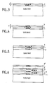
- the invention therefore consists in producing a structure such as that shown in FIG. 3 in which a layer 1 of superconductive material is covered with a layer 2 of material with different electrical characteristics, the two layers being different by the substitution of a Rare Earth element by another Rare Earth element so that the two materials have the same structure.
- the layer 1 of superconductive material being of the TR Ba2Cu3O 7-y type with TR chosen so that the material is superconductive with a high critical temperature Tc
- layer 2 is produced by replacing the rare earth TR with Lanthanum or Praseodymium or by substituting a small amount of Scandium for the rare earth TR.
- any other substitution can be made with other materials, we then obtain, depending on the substitution: - either an insulating layer 2 (I in FIG. 3), - or a layer 2 of weaker superconductivity than that of layer 1 (S ′ in FIG. 3).
- the layers 1 and 2 are thin layers and, in particular, the layer 2 has a thickness e of a few atomic layers.
- FIG. 4 represents a structure according to which two layers 1 and 3 of superconductive material enclose a layer 2 of a material with different electrical characteristics of identical constitution to that of layer 2 of FIG. 3.
- the layer 2 is then either insulating ( I) either normal metallic (N) or weakly superconductive (S ′).
- FIG. 5 represents a structure according to which it is a layer 1 of superconductive material which is enclosed by two layers 2 and 4 of material electrically different from layer 1.
- These layers 2 and 4 are similar to layer 2 of the structure of figure 3. They can be insulating (I), normal metallic (N) or weakly superconductive (S ′).
- the two layers 2 and 4 can be different.
- layer 2 can be insulating (I) and layer 4 weakly superconductive (S ′) or vice versa.
- FIG. 6 represents a structure comprising an alternation of superconductive layers (1, 3, 3 ′, ... n) and of layers (2, 2 ′, ...) of material electrically different from the superconductive material.
- These layers (2, 2 ′ 7) can thus be separately either insulating, or metallic, or slightly superconductive.
- the thin layers of superconductive oxides can be produced by molecular beam epitaxy as described in French patent application No. 87 09462 having as its title: "Process for producing thin film devices of superconductive materials and devices produced by this process "by G. CREUZET and A.FRIEDERICH.
- this patent application provides for making such layers by epitaxy, on a substrate, of the different constituent elements by regulating the admission of the different constituents to obtain a superconductive layer whose mesh parameter is substantially adapted to that of the substrate.
- Epitaxy can also be done directly from a superconductive material.
- the structures described above in relation to FIGS. 3 to 6 can be produced by momentary interruption of growth by epitaxy by molecular jets of the superconductor S when it is desired to produce a non-superconductive layer (I, N or S ′).
- a superconductor for example, of the following general formula: TR Ba2 Cu3 O 7-y where TR indicates a rare earth
- the conditions are modified in the following way: in the case where TR is substituted by La or Pr, one will close during a time corresponding to some atomic layers the cell of TR, and one will open in a synchronized way the La or Pr cell.
- the reverse operation will be carried out to resume growth of the superconductor in order to produce the second electrode.
- the Sc cell will be opened by simultaneously decreasing the power of the TR cell in order to achieve the partial substitution in the desired proportions, where the amount of Sc is minimized in order to maintain the structure.
- the invention extends to any process making it possible to destroy or reduce the superconductive properties of a material such as TR Ba2Cu3O 7-y by chemical modification of one or more elements in the process of growth and over a few atomic distances.
- the transport of the elements (Ba, Cu) in the form of a fluorinated compound (BaF2, CuF2) leading to total or partial occupation of the oxygen sites by the Fluoride without alteration of the crystal structure is included in the process.
- planar doping would consist, for example, of introducing a monolayer of Pr or La on the surface of the superconductor S, then of resuming the epitaxy of the superconductor on this monolayer.
- the process of the invention extends to sandwich structures where several layers are epitaxied in order to then produce complex systems of junctions. We then arrive at structures of the S - N - S - N - S - type as described in FIG. 6.
- the method of the invention also extends to the possibility of producing encapsulation layers impermeable to oxygen over the structures described above.
- the encapsulation layers are similar to those described in the patent of G.CREUZET and A.FRIEDERICH, July 87, already described previously.
- the invention resides mainly in the fact that a barrier made of non-superconductive material is produced by substitution of one of the constituents of the superconductive material on a few atomic layers, or in such a way that the very thin films thus produced have electrical properties such as insulator, normal metal, or weak superconductor.
- An intermediate layer of a junction comprising a first superconductive electrode by total substitution of TR with La or Pr, or by substitution of a small amount of Sc for TR. This operation is carried out on a few atomic layers, and the growth of the superconductive material is then resumed under normal conditions in order to produce a second superconductive electrode. This operation is carried out with structural continuity on both sides of the barrier. This substitution (total or partial) is of planar type because it only concerns a few atomic planes.
- the intermediate compound is not superconductive but has metallic properties.
- the junction is therefore of SNS type.
- the invention extends to any substitution of the same kind for another element which may lead to a junction of the SIS or SS′S type.
Landscapes
- Chemical & Material Sciences (AREA)
- Engineering & Computer Science (AREA)
- Ceramic Engineering (AREA)
- Superconductor Devices And Manufacturing Methods Thereof (AREA)
Applications Claiming Priority (2)
| Application Number | Priority Date | Filing Date | Title |
|---|---|---|---|
| FR8801163 | 1988-02-02 | ||
| FR8801163A FR2626715B1 (fr) | 1988-02-02 | 1988-02-02 | Dispositif en couches minces de materiau supraconducteur et procede de realisation |
Publications (1)
| Publication Number | Publication Date |
|---|---|
| EP0329507A1 true EP0329507A1 (de) | 1989-08-23 |
Family
ID=9362845
Family Applications (1)
| Application Number | Title | Priority Date | Filing Date |
|---|---|---|---|
| EP89400267A Withdrawn EP0329507A1 (de) | 1988-02-02 | 1989-01-31 | Dünnschichtanordnung aus supraleitendem Material und Verfahren zu ihrer Herstellung |
Country Status (4)
| Country | Link |
|---|---|
| US (1) | US5106823A (de) |
| EP (1) | EP0329507A1 (de) |
| JP (1) | JPH01272171A (de) |
| FR (1) | FR2626715B1 (de) |
Cited By (17)
| Publication number | Priority date | Publication date | Assignee | Title |
|---|---|---|---|---|
| EP0342038A2 (de) * | 1988-05-11 | 1989-11-15 | Canon Kabushiki Kaisha | Josephson-Einrichtung |
| WO1990000815A1 (de) * | 1988-07-06 | 1990-01-25 | Siemens Aktiengesellschaft | Josephson-tunnelelement mit metalloxidischem supraleitermaterial und verfahren zur herstellung des elementes |
| EP0371481A2 (de) * | 1988-11-29 | 1990-06-06 | Ube Industries, Ltd. | Laminierter Film und Methode zu dessen Herstellung |
| EP0422407A2 (de) * | 1989-10-13 | 1991-04-17 | International Business Machines Corporation | Mehrlagen-gitterdefekte Kupferoxyd-Perovkitstrukturen |
| EP0427640A1 (de) * | 1989-11-10 | 1991-05-15 | Sumitomo Electric Industries, Ltd. | Tunnelübergangsanordnung mit supraleitendem Oxydverbundmaterial |
| EP0430798A2 (de) * | 1989-11-27 | 1991-06-05 | Sumitomo Electric Industries, Ltd. | Tunnelübergangseinrichtung aus oxydisch supraleitendem Verbindungsmaterial und Methode zu ihrer Herstellung |
| DE4010489A1 (de) * | 1990-03-31 | 1991-10-02 | Dornier Luftfahrt | Supraleitendes element |
| EP0465326A2 (de) * | 1990-06-28 | 1992-01-08 | Sumitomo Electric Industries, Ltd. | Supraleitende Dünnschicht-Oxydverbindung und Verfahren zu deren Herstellung |
| EP0468868A2 (de) * | 1990-07-19 | 1992-01-29 | Sumitomo Electric Industries, Ltd. | Supraleitende Einrichtung mit geschichteter Struktur, zusammengesetzt aus oxidischem Supraleiter und Isolatordünnschicht und deren Herstellungsmethode |
| EP0476617A2 (de) * | 1990-09-18 | 1992-03-25 | Sumitomo Electric Industries, Limited | Supraleitende Übergangsstruktur und Verfahren zu deren Herstellung |
| WO1992005591A1 (en) * | 1990-09-21 | 1992-04-02 | The Regents Of The University Of California | Improved microelectronic superconducting devices and methods |
| EP0486404A2 (de) * | 1990-11-15 | 1992-05-20 | EASTMAN KODAK COMPANY (a New Jersey corporation) | Verbesserte Konstruktion von Hochtemperatur Supraleiter Übergangsanordnungen |
| EP0509886A2 (de) * | 1991-04-09 | 1992-10-21 | Sumitomo Electric Industries, Ltd. | Verfahren zum Strukturieren mehrlagiger Dünnschichten mit einer supraleitenden Lage |
| EP0543585A2 (de) * | 1991-11-15 | 1993-05-26 | The Hokkaido Electric Power Company Inc. | Verfahren zur Herstellung eines Oxidfilms |
| US5347143A (en) * | 1991-05-17 | 1994-09-13 | Dornier Luftfahrt Gmbh | Tunnelling barrier between two non-tunnelling superconductor-insulator-controlling superconductor-insulator-superconductor structures |
| US5747427A (en) * | 1991-11-15 | 1998-05-05 | Hokkaido Electric Power Co., Inc. | Process for forming a semiconductive thin film containing a junction |
| WO2000022652A2 (en) * | 1998-09-14 | 2000-04-20 | The Regents Of The University Of California | Superconducting structure including mixed rare earth barium-copper compositions |
Families Citing this family (24)
| Publication number | Priority date | Publication date | Assignee | Title |
|---|---|---|---|---|
| US5034359A (en) * | 1988-04-08 | 1991-07-23 | Kabushiki Kaisha Toshiba | Insulating composition |
| US5306699A (en) * | 1988-08-31 | 1994-04-26 | Superconductor Technologies, Inc. | Reactor vessel for manufacture of superconducting films |
| JPH02125672A (ja) * | 1988-11-04 | 1990-05-14 | Sanyo Electric Co Ltd | ジョセフソン接合素子及びその製造方法 |
| JPH02260674A (ja) * | 1989-03-31 | 1990-10-23 | Sumitomo Electric Ind Ltd | トンネル型ジョセフソン素子とその作製方法 |
| US5627139A (en) * | 1990-09-24 | 1997-05-06 | The Regents Of The University Of California | High-temperature superconducting josephson devices having a barrier layer of a doped, cubic crystalline, conductive oxide material |
| US5721196A (en) * | 1991-02-12 | 1998-02-24 | Sumitomo Electric Industries, Ltd. | Stacked tunneling and stepped grain boundary Josephson junction |
| JPH0570105A (ja) * | 1991-09-17 | 1993-03-23 | Sumitomo Electric Ind Ltd | 酸化物超電導薄膜 |
| JPH0575171A (ja) * | 1991-09-17 | 1993-03-26 | Sumitomo Electric Ind Ltd | 超電導接合 |
| JPH0585705A (ja) * | 1991-09-26 | 1993-04-06 | Sumitomo Electric Ind Ltd | 酸化物超電導薄膜 |
| WO1993010565A1 (en) * | 1991-11-13 | 1993-05-27 | Seiko Epson Corporation | Superconductive element |
| US5593950A (en) * | 1992-07-28 | 1997-01-14 | Nippon Telegraph & Telephone Corporation | Lattice matching super conducting device with a- and c- axes |
| US5479059A (en) * | 1993-08-23 | 1995-12-26 | United Technologies Corporation | Thin film superconductor magnetic bearings |
| JPH0782080A (ja) * | 1993-09-13 | 1995-03-28 | Kokusai Chodendo Sangyo Gijutsu Kenkyu Center | 酸化物超電導体単結晶薄膜作製法 |
| JPH07263767A (ja) | 1994-01-14 | 1995-10-13 | Trw Inc | イオンインプランテーションを用いたプレーナ型の高温超伝導集積回路 |
| FR2724769B1 (fr) * | 1994-09-16 | 1996-12-06 | Thomson Csf | Procede de realisation de diodes laser a emission surfacique |
| US5831278A (en) * | 1996-03-15 | 1998-11-03 | Conductus, Inc. | Three-terminal devices with wide Josephson junctions and asymmetric control lines |
| US6541136B1 (en) * | 1998-09-14 | 2003-04-01 | The Regents Of The University Of California | Superconducting structure |
| US6147032A (en) | 1999-05-19 | 2000-11-14 | Trw Inc. | Method for indirect Ion implantation of oxide superconductive films |
| US6188919B1 (en) | 1999-05-19 | 2001-02-13 | Trw Inc. | Using ion implantation to create normal layers in superconducting-normal-superconducting Josephson junctions |
| US6624122B1 (en) * | 2000-06-21 | 2003-09-23 | The Regents Of The University Of California | High critical current superconducting tapes |
| JP3425422B2 (ja) | 2000-10-31 | 2003-07-14 | 株式会社東芝 | 超電導素子の製造方法 |
| US6699820B2 (en) * | 2001-03-02 | 2004-03-02 | Hartmut Ulrich Bielefeldt | Method for making a superconductor with enhanced current carrying capability |
| US7615385B2 (en) | 2006-09-20 | 2009-11-10 | Hypres, Inc | Double-masking technique for increasing fabrication yield in superconducting electronics |
| US8204564B2 (en) * | 2007-11-07 | 2012-06-19 | Brookhaven Science Associates, Llc | High temperature interfacial superconductivity |
Citations (2)
| Publication number | Priority date | Publication date | Assignee | Title |
|---|---|---|---|---|
| FR2469005A1 (fr) * | 1979-11-05 | 1981-05-08 | Nippon Telegraph & Telephone | Jonction josephson de supraconducteurs a base d'oxyde et son procede de fabrication |
| DE3810243A1 (de) * | 1987-03-25 | 1988-10-06 | Hitachi Ltd | Supraleitende duennfilme und verfahren zu ihrer herstellung |
Family Cites Families (2)
| Publication number | Priority date | Publication date | Assignee | Title |
|---|---|---|---|---|
| US4905319A (en) * | 1987-07-28 | 1990-02-27 | Syracuse University | Superconducting device including a thin chromium film with negative susceptibility |
| US4869598A (en) * | 1988-03-11 | 1989-09-26 | Mcdonald Donald G | Temperature-sensitive multiple-layer thin film superconducting device |
-
1988
- 1988-02-02 FR FR8801163A patent/FR2626715B1/fr not_active Expired - Lifetime
-
1989
- 1989-01-31 EP EP89400267A patent/EP0329507A1/de not_active Withdrawn
- 1989-02-02 JP JP1024758A patent/JPH01272171A/ja active Pending
-
1991
- 1991-06-06 US US07/711,391 patent/US5106823A/en not_active Expired - Fee Related
Patent Citations (2)
| Publication number | Priority date | Publication date | Assignee | Title |
|---|---|---|---|---|
| FR2469005A1 (fr) * | 1979-11-05 | 1981-05-08 | Nippon Telegraph & Telephone | Jonction josephson de supraconducteurs a base d'oxyde et son procede de fabrication |
| DE3810243A1 (de) * | 1987-03-25 | 1988-10-06 | Hitachi Ltd | Supraleitende duennfilme und verfahren zu ihrer herstellung |
Non-Patent Citations (5)
| Title |
|---|
| APPLIED PHYSICS LETTERS, vol. 51, no. 7, 17 août 1987, pages 540-541, American Institute of Physics, New York, US; J. MORELAND et al.: "Josephson effect above 77 K in a YBaCuO break junction" * |
| JAPANESE JOURNAL OF APPLIED PHYSICS, vol. 26, no. 5, mai 1987, pages L815-L817, Tokyo, JP; S. OHSHIMA et al.: "Superconducting and structural properties of the new Ba1-xLnxCuO3-y compound system (Ln=La, Ce, Pr, Nd, Sm, Eu, Gd, Tb, Dy, Ho, Er and Yb) * |
| PHYSICAL REVIEW LETTERS, vol. 59, no. 10, 7 septembre 1987, pages 1160-1163, The American Physical Society, New York, US; T.K. WORTHINGTON et al.: "Anisotropic nature of high-temperature superconductivity in single-crystal Y1Ba2Cu3O7-x" * |
| SOLID STATE COMMUNICATIONS, vol. 63, no. 5, 1987, pages 409-410, Pergamon Journals Ltd, Oxford, GB; B.R. ZHAO et al.: "The effect of Sc on the superconductivity of the Ba-Y-Cu oxides" * |
| SOLID STATE COMMUNICATIONS, vol. 63, no. 6, 1987, pages 515-519, Pergamon Journals Ltd, Oxford, GB; K.N. YANG et al.: "High temperature superconductivity in rare-earth (R)-Barium copper oxides(RBa2)Cu3O9.delta" * |
Cited By (31)
| Publication number | Priority date | Publication date | Assignee | Title |
|---|---|---|---|---|
| EP0342038A2 (de) * | 1988-05-11 | 1989-11-15 | Canon Kabushiki Kaisha | Josephson-Einrichtung |
| EP0342038A3 (en) * | 1988-05-11 | 1990-01-10 | Canon Kabushiki Kaisha | Josephson device |
| WO1990000815A1 (de) * | 1988-07-06 | 1990-01-25 | Siemens Aktiengesellschaft | Josephson-tunnelelement mit metalloxidischem supraleitermaterial und verfahren zur herstellung des elementes |
| EP0371481A2 (de) * | 1988-11-29 | 1990-06-06 | Ube Industries, Ltd. | Laminierter Film und Methode zu dessen Herstellung |
| EP0371481A3 (en) * | 1988-11-29 | 1990-08-22 | Ube Industries, Ltd. | Laminated film and method for producing the same |
| EP0422407A3 (en) * | 1989-10-13 | 1991-08-07 | International Business Machines Corporation | Multilayer distorted-lattice copper-oxide perovskite structures |
| EP0422407A2 (de) * | 1989-10-13 | 1991-04-17 | International Business Machines Corporation | Mehrlagen-gitterdefekte Kupferoxyd-Perovkitstrukturen |
| US5529980A (en) * | 1989-10-13 | 1996-06-25 | International Business Machines Corporation | Multilayer distorted-lattice copper-oxide perovskite structures including NdCeCuO and YBaCuO multi-layers |
| EP0427640A1 (de) * | 1989-11-10 | 1991-05-15 | Sumitomo Electric Industries, Ltd. | Tunnelübergangsanordnung mit supraleitendem Oxydverbundmaterial |
| EP0430798A2 (de) * | 1989-11-27 | 1991-06-05 | Sumitomo Electric Industries, Ltd. | Tunnelübergangseinrichtung aus oxydisch supraleitendem Verbindungsmaterial und Methode zu ihrer Herstellung |
| EP0430798A3 (en) * | 1989-11-27 | 1991-09-11 | Sumitomo Electric Industries, Ltd. | Tunnel junction device composed of compound oxide superconductor material and method for fabricating the same |
| DE4010489A1 (de) * | 1990-03-31 | 1991-10-02 | Dornier Luftfahrt | Supraleitendes element |
| EP0465326A3 (en) * | 1990-06-28 | 1992-04-15 | Sumitomo Electric Industries, Ltd. | Superconducting thin film of compound oxide and a process for preparing the same |
| EP0465326A2 (de) * | 1990-06-28 | 1992-01-08 | Sumitomo Electric Industries, Ltd. | Supraleitende Dünnschicht-Oxydverbindung und Verfahren zu deren Herstellung |
| EP0468868A2 (de) * | 1990-07-19 | 1992-01-29 | Sumitomo Electric Industries, Ltd. | Supraleitende Einrichtung mit geschichteter Struktur, zusammengesetzt aus oxidischem Supraleiter und Isolatordünnschicht und deren Herstellungsmethode |
| US5422497A (en) * | 1990-07-19 | 1995-06-06 | Sumitomo Electric Industries, Ltd. | Superconducting device having layered structure composed of oxide thin film and insulator thin film |
| EP0468868A3 (en) * | 1990-07-19 | 1992-05-27 | Sumitomo Electric Industries, Ltd. | Superconducting device having layered structure composed of oxide superconductor thin film and insulator thin film and method for manufacturing the same |
| EP0476617A2 (de) * | 1990-09-18 | 1992-03-25 | Sumitomo Electric Industries, Limited | Supraleitende Übergangsstruktur und Verfahren zu deren Herstellung |
| EP0476617A3 (en) * | 1990-09-18 | 1992-07-22 | Sumitomo Electric Industries, Limited | Superconductor junction structure and process for fabricating the same |
| WO1992005591A1 (en) * | 1990-09-21 | 1992-04-02 | The Regents Of The University Of California | Improved microelectronic superconducting devices and methods |
| US5256636A (en) * | 1990-09-21 | 1993-10-26 | The Regents Of The University Of Calif. | Microelectronic superconducting device with multi-layer contact |
| EP0486404A3 (en) * | 1990-11-15 | 1992-11-04 | Eastman Kodak Company (A New Jersey Corporation) | Improved construction of high temperature josephson junction device |
| EP0486404A2 (de) * | 1990-11-15 | 1992-05-20 | EASTMAN KODAK COMPANY (a New Jersey corporation) | Verbesserte Konstruktion von Hochtemperatur Supraleiter Übergangsanordnungen |
| EP0509886A3 (en) * | 1991-04-09 | 1993-01-27 | Sumitomo Electric Industries, Ltd. | Process for patterning layered thin films including a superconductor layer |
| EP0509886A2 (de) * | 1991-04-09 | 1992-10-21 | Sumitomo Electric Industries, Ltd. | Verfahren zum Strukturieren mehrlagiger Dünnschichten mit einer supraleitenden Lage |
| US5347143A (en) * | 1991-05-17 | 1994-09-13 | Dornier Luftfahrt Gmbh | Tunnelling barrier between two non-tunnelling superconductor-insulator-controlling superconductor-insulator-superconductor structures |
| EP0543585A2 (de) * | 1991-11-15 | 1993-05-26 | The Hokkaido Electric Power Company Inc. | Verfahren zur Herstellung eines Oxidfilms |
| EP0543585A3 (de) * | 1991-11-15 | 1993-06-02 | The Hokkaido Electric Power Company Inc. | Verfahren zur Herstellung eines Oxidfilms |
| US5747427A (en) * | 1991-11-15 | 1998-05-05 | Hokkaido Electric Power Co., Inc. | Process for forming a semiconductive thin film containing a junction |
| WO2000022652A2 (en) * | 1998-09-14 | 2000-04-20 | The Regents Of The University Of California | Superconducting structure including mixed rare earth barium-copper compositions |
| WO2000022652A3 (en) * | 1998-09-14 | 2000-07-20 | Univ California | Superconducting structure including mixed rare earth barium-copper compositions |
Also Published As
| Publication number | Publication date |
|---|---|
| FR2626715A1 (fr) | 1989-08-04 |
| FR2626715B1 (fr) | 1990-05-18 |
| JPH01272171A (ja) | 1989-10-31 |
| US5106823A (en) | 1992-04-21 |
Similar Documents
| Publication | Publication Date | Title |
|---|---|---|
| EP0329507A1 (de) | Dünnschichtanordnung aus supraleitendem Material und Verfahren zu ihrer Herstellung | |
| Lee et al. | Epitaxially grown sputtered LaAlO3 films | |
| US5696392A (en) | Barrier layers for oxide superconductor devices and circuits | |
| US6011981A (en) | Oxide superconductor multilayered film and oxide superconductor josephson device | |
| EP0511056B1 (de) | Josephsonjunctionstruktur | |
| EP0390704B1 (de) | Josephsoneffektbauelement des Typs mit Tunnelverbindung und Verfahren zu seiner Herstellung | |
| US5627139A (en) | High-temperature superconducting josephson devices having a barrier layer of a doped, cubic crystalline, conductive oxide material | |
| CA2029662C (en) | Tunnel junction device using compound oxide superconductor material | |
| US6229154B1 (en) | Photo detecting element | |
| EP0458013B1 (de) | Aufbaustruktur einer supraleitenden Einrichtung bei Nutzung der Anisotropie der materialspezifischen Energielücke | |
| JPH104223A (ja) | 酸化物超電導体ジョセフソン素子 | |
| US5422338A (en) | Layer-by-layer vapor deposition method for forming a high Tc superconductor thin film device | |
| EP0325526A2 (de) | Aus supraleitendem Material hergestellte Anordnung und Verfahren zu deren Herstellung | |
| EP0491496B1 (de) | Artikel mit supraleiter/isolator Lagenstruktur und Verfahren zur Herstellung des Artikels | |
| JP2831967B2 (ja) | 超電導素子 | |
| US20040134967A1 (en) | Interface engineered high-Tc Josephson junctions | |
| Horiuchi et al. | Superconductivity of strained YBa2Cu3O7/(La1-xSrx) 2CuO4 superlattices | |
| JPH0272685A (ja) | 超伝導弱結合部の形成方法 | |
| EP0461016B1 (de) | Supraleitendes zusammengesetztes Element und dessen Herstellungsverfahren | |
| JP2955641B2 (ja) | イン サイチュー型ジョセフソン接合構造 | |
| JPH06302872A (ja) | 酸化物超電導薄膜上に上層の薄膜を積層する方法 | |
| JP3155641B2 (ja) | 超伝導トンネル接合デバイス | |
| JP2774713B2 (ja) | 超電導素子 | |
| JP2861235B2 (ja) | 超伝導素子 | |
| JP2899287B2 (ja) | ジョセフソン素子 |
Legal Events
| Date | Code | Title | Description |
|---|---|---|---|
| PUAI | Public reference made under article 153(3) epc to a published international application that has entered the european phase |
Free format text: ORIGINAL CODE: 0009012 |
|
| AK | Designated contracting states |
Kind code of ref document: A1 Designated state(s): DE GB IT NL |
|
| 17P | Request for examination filed |
Effective date: 19900122 |
|
| 17Q | First examination report despatched |
Effective date: 19920407 |
|
| STAA | Information on the status of an ep patent application or granted ep patent |
Free format text: STATUS: THE APPLICATION IS DEEMED TO BE WITHDRAWN |
|
| 18D | Application deemed to be withdrawn |
Effective date: 19920801 |