EP0422407A2 - Mehrlagen-gitterdefekte Kupferoxyd-Perovkitstrukturen - Google Patents
Mehrlagen-gitterdefekte Kupferoxyd-Perovkitstrukturen Download PDFInfo
- Publication number
- EP0422407A2 EP0422407A2 EP90117715A EP90117715A EP0422407A2 EP 0422407 A2 EP0422407 A2 EP 0422407A2 EP 90117715 A EP90117715 A EP 90117715A EP 90117715 A EP90117715 A EP 90117715A EP 0422407 A2 EP0422407 A2 EP 0422407A2
- Authority
- EP
- European Patent Office
- Prior art keywords
- copper
- comparison
- perovskite material
- oxide
- nondistorted
- Prior art date
- Legal status (The legal status is an assumption and is not a legal conclusion. Google has not performed a legal analysis and makes no representation as to the accuracy of the status listed.)
- Withdrawn
Links
Images

Classifications
-
- H—ELECTRICITY
- H10—SEMICONDUCTOR DEVICES; ELECTRIC SOLID-STATE DEVICES NOT OTHERWISE PROVIDED FOR
- H10N—ELECTRIC SOLID-STATE DEVICES NOT OTHERWISE PROVIDED FOR
- H10N60/00—Superconducting devices
- H10N60/01—Manufacture or treatment
- H10N60/0268—Manufacture or treatment of devices comprising copper oxide
- H10N60/0296—Processes for depositing or forming copper oxide superconductor layers
- H10N60/0521—Processes for depositing or forming copper oxide superconductor layers by pulsed laser deposition, e.g. laser sputtering
-
- C—CHEMISTRY; METALLURGY
- C04—CEMENTS; CONCRETE; ARTIFICIAL STONE; CERAMICS; REFRACTORIES
- C04B—LIME, MAGNESIA; SLAG; CEMENTS; COMPOSITIONS THEREOF, e.g. MORTARS, CONCRETE OR LIKE BUILDING MATERIALS; ARTIFICIAL STONE; CERAMICS; REFRACTORIES; TREATMENT OF NATURAL STONE
- C04B35/00—Shaped ceramic products characterised by their composition; Ceramics compositions; Processing powders of inorganic compounds preparatory to the manufacturing of ceramic products
- C04B35/01—Shaped ceramic products characterised by their composition; Ceramics compositions; Processing powders of inorganic compounds preparatory to the manufacturing of ceramic products based on oxide ceramics
- C04B35/45—Shaped ceramic products characterised by their composition; Ceramics compositions; Processing powders of inorganic compounds preparatory to the manufacturing of ceramic products based on oxide ceramics based on copper oxide or solid solutions thereof with other oxides
- C04B35/4504—Shaped ceramic products characterised by their composition; Ceramics compositions; Processing powders of inorganic compounds preparatory to the manufacturing of ceramic products based on oxide ceramics based on copper oxide or solid solutions thereof with other oxides containing rare earth oxides
- C04B35/4508—Type 1-2-3
-
- H—ELECTRICITY
- H10—SEMICONDUCTOR DEVICES; ELECTRIC SOLID-STATE DEVICES NOT OTHERWISE PROVIDED FOR
- H10N—ELECTRIC SOLID-STATE DEVICES NOT OTHERWISE PROVIDED FOR
- H10N60/00—Superconducting devices
- H10N60/80—Constructional details
- H10N60/85—Superconducting active materials
- H10N60/855—Ceramic superconductors
- H10N60/857—Ceramic superconductors comprising copper oxide
- H10N60/858—Ceramic superconductors comprising copper oxide having multilayered structures, e.g. superlattices
-
- Y—GENERAL TAGGING OF NEW TECHNOLOGICAL DEVELOPMENTS; GENERAL TAGGING OF CROSS-SECTIONAL TECHNOLOGIES SPANNING OVER SEVERAL SECTIONS OF THE IPC; TECHNICAL SUBJECTS COVERED BY FORMER USPC CROSS-REFERENCE ART COLLECTIONS [XRACs] AND DIGESTS
- Y10—TECHNICAL SUBJECTS COVERED BY FORMER USPC
- Y10S—TECHNICAL SUBJECTS COVERED BY FORMER USPC CROSS-REFERENCE ART COLLECTIONS [XRACs] AND DIGESTS
- Y10S505/00—Superconductor technology: apparatus, material, process
- Y10S505/70—High TC, above 30 k, superconducting device, article, or structured stock
- Y10S505/701—Coated or thin film device, i.e. active or passive
Definitions
- the present invention broadly concerns copper-oxide perovskite materials. More particularly, the invention concerns copper-oxide perovskite superconductor materials having strained crystallographic lattices and altered superconductive properties.
- Superconductive copper-oxide perovskite materials have excited great interest because certain of these materials have transition temperatures to the superconductive state which are a higher than previously-known superconductive materials. Although such superconductive materials have transition temperatures and critical current densities which are high enough for many applications, the ability to alter and improve such parameters would be desirable.
- the present invention as claimed discloses a multilayered structure comprising copper-oxide perovskite material having strained crystallographic lattices and altered superconductive properties.
- the multilayer structure of the invention comprises at least one first layer of a first copper-oxide perovskite material and at least one second layer of a second copper-oxide perovskite material.
- the first and second layers are adjacent to one another in an epitaxial lattice-distortion relationship.
- the first copper-oxide perovskite material is different from the second copper-oxide perovskite material.
- the first copper-oxide perovskite material in an unstressed bulk state defines a first comparison nondistorted crystallagraphic lattice structure having first comparison nondistorted unit cell dimensions.
- the first copper-oxide perovskite material in the unstressed bulk state exhibits normal and superconductive states which define a set of comparison normal/superconducting transition parameters.
- the second copper-oxide perovskite material in an unstressed bulk state defines a second comparison nondistorted crystallographic lattice structure having second comparison nondistorted unit cell dimensions.
- the first and the second comparison nondistorted unit cell dimensions differ in at least one dimension.
- the difference in dimension is at least one percent in magnitude. Differences in dimension of three percent, five percent or even more in magnitude may be preferred in certain cases.
- the first copper-oxide perovskite material in the first layer has a first crystallographic lattice structure having first unit cell dimensions.
- the first crystallographic lattice structure is distorted relative to the first comparison nondistorted crystallographic lattice structure, with at least one first unit cell dimension differing by a lattice-distortion amount from a corresponding first comparison nondistorted unit cell dimension.
- the first copper-oxide perovskite material in at least one first layer exhibits normal and superconductive states which define a set of normal/superconducting transition parameters. At least one of the normal/superconducting transition parameters differs by a lattice-distortion amount from a corresponding comparison normal/superconducting transition parameter.
- the second copper-oxide perovskite material in the second layer has a second crystallographic lattice structure having second unit cell dimensions.
- the second crystallographic lattice structure is distorted relative to the second comparison nondistorted crystallographic lattice structure with at least one first unit cell dimension differing by a lattice-distortion amount from a corresponding second comparison nondistorted unit cell dimension.
- An advantage of certain preferred multilayer structures of the invention is that the critical current density is increased relative to the critical current density of a film composed of the material of any one of the layers.
- the compositions of YBa2Cu3O 7- ⁇ and GdBa2Cu3O 7- ⁇ -high current densities have been achieved.
- multilayer structure of the invention made up of alternating layers of the above two materials with each layer, a current-density value of about 4 x 10⁶ A/cm2 at about 81 K has been achieved.
- a particularly preferred multilayer structure of the invention about 100 nm thick made up of alternating layers of YBa2Cu3O 7- ⁇ and Nd 1.83 Ce 0.17 CuO 4 ⁇ y with each layer about 5 nm thick, has exhibited a critical current density of about 2 x 10⁶ A/cm2 at about 80 K. It is expected that high current densities will also be observed in the presence of high magnetic fields.
- multilayer structures of the invention are preferably prepared on (100) oriented SrTiO3 by a laser ablation deposition process.
- Two alternating ceramic targets are preferably used at a temperature in the range of from about 700 to about 720°C in about 200 mTorr oxygen.
- Conductivity in the copper-oxide perovskite superonductor material YBa2Cu3O 7- ⁇ occurs mainly in the crystallographic a-b plane.
- the highest critical currents in films of such material are also generally obtained when the films are fully oriented with their crystallographic c axis perpendicular to the substrate and have a minimal number of grain boundaries.
- epitaxial films which are polycrystalline with c-axes oriented generally perpendicular to the substrate and with random orientation in the a-b plane are also capable of carrying reasonably high critical currents.
- Multilayer structures of the invention can be prepared in a deposition chamber made of stainless steel which is generally cylindrical in shape with a cylinder axis extending vertically, roughly 200 mm in diameter and roughly 400 mm high.
- the chamber can have five approximately 100 mm in diameter with vacuum-tight joints flanges attached to them.
- a first flange is located at the top of the deposition chamber for a heated substrate holder.
- a second flange is located at the bottom for connecting a vacuum pump and pressure gauges three flanges are located in an essentially horizontal plane passing midway through the deposition chamber. Axes passing through the three flanges define angles of about 0°, 90° and 135°.
- a rotable dual target holder which can hold two ceramic respectively of pellets respectively of Y Ba2Cu3O 7- ⁇ and Nd 1.83 Ce 0.17 CuO 4 ⁇ y , about 3 mm thick and about 25 mm in diameter.
- the other two flanges have fused silica windows about 100 mm in diameter, one for admitting an incoming laser beam at approximately 135° to the surface of the target, and the other to enable side viewing of the plume ablated from the target material and for viewing the substrates when rotated at about 90° to face this window.
- Pyrometric determination of the substrate surface temperatures can readily be carried out at the end of each deposition run using an infrared pyrometer since the surfaces of the hot films are black.
- the infrared pyrometer temperature measurements can be confirmed by a direct measurement of the film surface temperature, performed with the aid of a small thermocouple attached to the surface of the film.
- An additional thermocouple can be imbedded in the body of a resistively-heated stainless-steel sample holder, which could be heated to 900°C.
- the substrates can be approximately rectangular in shape, about 4 mm x 8 mm.
- the substrates can be glued to the heated sample holder with a silver paste for good thermal contact.
- Two target pellets can be located on the rotable target holder, with one or the other target pellet rotated to a position facing the substrates and substantially parallel to their surface at a distance of about 45 mm.
- a laser ablation technique can be used to deposit high quality films of YBa2Cu3O 7- ⁇ and Nd 1.83 Ce 0.17 CuO 4 ⁇ y on (100) oriented strontium titanate substrates.
- the relatively close lattice match along the crystallographic a and b-axis of the tetragonal neodymium cerium copper oxide (0,395 nm) with the lattice constant of cubic strontium titanate (0,3905 nm) makes the (100) cut of SrTiO3 suitable for growth of epitaxial films of the oxide.
- Pulses of an excimer laser wavelength of about 248 nm and a pulse duration of about 8 ns having a can be used for the ablation process.
- Two targets can be used, one as a source for the yttrium barium copper oxide layers and the other for the neodymium cerium copper oxide layers.
- the neodymium cerium copper oxide target can be an approximately 25-mm diameter sintered pellet of Nd 1.83 Ce 0.17 CuO4 prepared from a mixture of CeO2, Nd2O3 and CuO in proportions to give the desired stoichiometry.
- the powder can first calcined in air at about 900°C for about 32 hrs. The calcined powder can then be pressed into a pellet and sintered at about 1050°C in air for about 16 hrs and then furnace cooled to room temperature.
- the yttrium barium copper oxide target can be an approximately 25-mm diameter sintered pellet of YBa2Cu 3O7 prepared from a mixture of Y2O3, BaCO3 and CuO in proportions to give the desired stoichiometry.
- the mixture can be heated in oxygen at about 925°C for about 8 hours.
- the resulting material is then reground, pressed into a pellet, and heated to about 900°C in air for about 16 hours.
- the pellet may then be furnace cooled slowly to room temperature over eight hours.
- the laser pulse repetition rate is variable over the range of from about 1 Hz to 2 Hz.
- the 1 Hz pulse repetition rate is preferred for thicker films, say 20 nm thick, the 2-N2 pulse repitition rate is preferred.
- the laser beam can be focused down to an area of about 2.5 mm by about 1.5 mm on the surface of the target to produce fluences in the range of from about 2.00 J/cm2 to about 3.5 J/cm2. Fluences in the range of from about 2.5 to about 3.0 J/cm2 are particularly preferred.
- the focusing lens can be continuously rastered over an area about 6mm by about 6mm of the target.
- the focusing lens can be mounted on a translation stage and programmed to move horizontally and vertically so as to translate the laser beam in a zig-zag pattern on the pellet. In this way a film thickness uniform to within about ⁇ 5 percent over an area of about 15 mm by about 15 mm can generally be obtained.
- the laser-produced plume for the yttrium barium copper oxide target in about about 200 mTorr O2 ambient was purplish in color and had a cross section of about 20 mm diameter on the substrates.
- An oxygen pressure of about 200 mTorr is maintained in the chamber.
- a cone-shaped bluish white plume is produced.
- the plume can have a cross section of about 20 mm diameter on substrates placed at a distance of about 45 mm from the target.
- a vacuum base pressure of about 2 x 10 ⁇ 6 Torr, together with a few O2 flushing cycles prior to each deposition run can be used.
- the substrate surface temperature can be kept at about 730°C and the O2 pressure in the cell at about 200 mTorr.
- Alternating layers of Nd 1.83 Ce .17 Cu O 4 ⁇ y and YBa2Cu3O7- ⁇ can be deposited on the substrate by alternately positioning the neodymium cerium copper oxide pellet and the yttrium barium copper oxide pellet in the path of the laser beam using the rotatable target holder.
- Occasional O2 flushings can be employed to reduce the accumulation of particulates in the deposition chamber.
- oxygen to about 1 atm can be added slowly to the chamber while the substrate temperature is simultaneously lowered slowly to about 400°C.
- the films can be left at this temperature for half an hour and then slowly cooled down to room temperature.
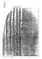
- a transmission electron micrograph shows a multilayer epitaxial neodymium cerium copper oxide/yttrium barium copper oxide structure 2 on a strontium titanate substrate 4.
- the multilayer structure 2 includes alternate layers 6 of Nd 1.83 Ce .17 Cu O4 ⁇ y which appear as dark bands in the transmission electron micrograph of Figure 1.
- Alternating with the neodymium cerium copper oxide layers 6 are layers 8 of YBa2Cu3O 7- ⁇ - which appear as light bands on the transmission electron micrograph of Figure 1.
- the neodymium cerium copper oxide layers 6 are approximately 20 nm thick.
- the yttrium barium copper oxide layers 8 are approximately 25 nm thick.
- Striations may be seen in both the neodymium cerium copper oxide layers 6 and in the yttrium barium copper oxide layers 8 in Figure 1.
- the striations are evidently images of individual copper-oxide planes in the two copper oxide perovskite materials.
- the regularity of the striations and their extent are evidence that both the neodymium cerium copper oxide layers 6 and the yttrium barium copper oxide layers 8 are epitaxial in structure with the crystallagraphic c axis extending normal to the striations in the plane of the Figure.
- the 20 nm thickness of the neodymium cerium copper oxide layers 6 corresponds to approximately 16 atomic planes.
- the 25 nm thickness of the layers of yttrium barium copper oxide 8 corresponds to approximately 21 atomic planes.
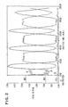
- FIG 2 an Auger electron spectroscopic ("AES") profile of a multilayer structure of the present invention on a strontium titanate substrate is shown.
- the AES profile of Figure 2 includes three atomic concentration traces: a titanium concentration trace 10 which represents an atomic concentration of titanium, a neodymium concentration trace 12 which represents an atomic concentration of neodymium, and a barium concentration trace 14 concentration which represents an atomic concentration of barium.
- the three traces 10, 12, 14 are given as a function of sputtering time, which corresponds to a depth within the multilayer structure.
- the atomic concentration of barium in the sample varies as a function of depth in an approximately rectangular-pulsed fashion between relatively a low and a relatively high value.
- the rouding of the rectangular pulses is believed to be due to the non-zero escape depth of the Auger electrons detected by the AES spectrometer.
- the neodymium concentration also varies in an approximately rectangular-pulsed fashion as a function of depth between a relatively low and a relatively high value.
- the barium and neodymium concentrations vary essentially out of phase with one another and evidence a relatively sharp transition from one concentration to the other, which indicates that the sample is made up of neo-denium-containing layers alternating with barium-containing layers.
- the profile of Figure 2 also indicates that the concentration of titanium was essentially zero to the depth sampled.
- the Auger electron spectroscopic profile of Figure 2 is consistent with the interpretation that the sample was essentially made up of alternating layers of neodymium cerium copper oxide and yttrium barium copper oxide.
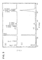
- Figure 3 shows x-ray defraction patterns of two samples of multilayer structures of neodymium cerium copper oxide layers alternated with layers of yttrium barium copper oxide.
- each layer was approximately 20 nm thick.
- each layer was approximately 40 nm thick. The reduced number of peaks in the lower diffraction pattern relative to the number of peaks in the upper pattern indicates that the crystallographic lattices of the samples for the respective diffraction patterns differ.
- the relatively fewer number of peaks in the upper diffraction pattern indicate that the lattice of the yttrium barium copper oxide material and the lattice of the neodymium cerium copper oxide material distorted one another to form intermediate lattice structures closely similar to each other.
- the alternating layers of materials exhibit a coherency strain.
- the relatively greater number of peaks indicate that at the 40 nm layer thickness, the two materials did not distort to form similar intermediate structures.
- the layers of materials at the 40 nm thickness evidently developed misfit dislocations and relaxed 40 noncoherency strained structures.
- FIG 4 graphs of the resistivity versus temperature of four films of copper oxide material deposited on a strontium titanate substrate is one shown. Each of the four films is roughly 100 nm thick.
- the films consist variously of Nd 1.83 Ce 0.17 CuO 4 ⁇ y and YBa2Cu3O 7- ⁇ , either alone or in multilayer structures of alternating layers of the two materials.
- the neodymium cerium copper oxide material and the yttrium barium copper material were deposited by laser ablation under substantially the same conditions.
- Trace 20 on Figure 4 is a graph of the resistivity versus temperature of a sample of essentially pure YBa2Cu3O 7- ⁇ .
- the resistivity of the sample decreases approximately linearly with absolute temperature to a transition temperature of about 93 K, where the resistivity drops sharply to zero.
- the film of yttrium barium copper oxide is thus superconductive below the transition temperature.
- Undistorted bulk YBa2Cu3O 7- ⁇ has an orthorhombic crystal structure, with the "a" and "b" unit cell dimensions of approximately 0,383 nm and 0,388 nm, respectively, for ⁇ close to zero.
- Trace 22 on Figure 4 is a graph of a film of neodymium cerium copper oxide.
- the resistivity drops to a minimum at roughly 100 K and then increases gradually as the temperature decreases further.
- the neodymium cerium copper oxide film is not superconductive at least down to approximately 5 K.
- Undistorted bulk Nd 1.83 Ce 0.17 CuO 4 ⁇ y has a tetragonal crystal structure, with the "a" and "b" unit-cell dimensions both approximately equal to 0,395 nm.
- Trace 24 on Figure 4 is a graph of the resistivity versus temperature of multilayer structure of alternate layers of Nd 1.80 Ce 0.17 CuO 4 ⁇ y and YBa2Cu3O 7- ⁇ on a (100) strontium titanate substrate.
- the multilayer structure has three layers of each material for a total of six layers. Each of the layers is approximately 20 nm thick.
- the resistivity decreases approximately linearly from about 300 K to a transition temperature of approximately 89 K, where the resistivity drops sharply to zero.
- the crystallographic lattices of both the neodynium cerium copper oxide layers and the yttrium barium copper oxide layers are distorted relative to the in bulk crystal structures.
- the "a" and "b" unit cell dimensions in both distorted crystallographic lattices are approximately equal to 0,388 nm.
- Trace 26 in Figure 4 is a graph of the resistivity versus temperature of a multilayer structure of alternate layers of Nd 1.83 Ce 0.17 CuO 4 ⁇ y and YBa2Cu3O 7- ⁇ on a (100) strontium titanate substrate.
- the multilayer structure has a total of twenty layers, with ten layers being composed of each copper oxide. Each of the layers is approximately 5 nm thick.
- the resistivity is seen to be greater than the films of traces 20 and 24.
- the resistivity drops substantially linearly as a function of temperature from about 300K to a transition temperature of approximately 89K, then drops to zero.
- the crystallographic lattices of both the neodymium cerium copper oxide layers and the yttrium barium copper oxide layers are distorted, with the "a" and "b" unit-cell dimensions approximately equal to 0,388 nm.
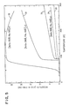
- FIG. 5 graphs of the resistivity versus temperature of five films of copper oxide material deposited on a strontium titanate substrate is one shown.
- the films consist variously and YBa2Cu3O 7- ⁇ either alone or in multilayer structures with alternating layers of Nd 1.83 Ce 0.17 CuO 4 ⁇ y .
- the neodymium cerium copper oxide material and the yttrium barium copper material were deposited by laser ablation under substantially the same conditions. Traces 20, 22, and 24 from Figure 4 are reproduced on Figure 5 for purposes of comparison.
- Trace 28 on Figure 5 is a graph of the resistivity versus temperature of multilayer structure of alternate layers of Nd 1.83 Ce 0.17 CuO 4 ⁇ y and YBa2Cu3O 7- ⁇ on a (100) strontium titanate substrate.
- the multilayer structure has five layers of each material for a total of ten layers.
- Each of the layers of the yttrium barium copper oxide material is approximately 10 nm thick.
- Each of the layers of the neodymium cerium copper oxide material is approximately 20 nm thick.
- the resistivity decreases from about 275 K to a transition temperature of approximately 83 K, where the resistivity drops to zero.
- the superconductive transition is broad relative to that of trace 24 for example.
- crystallographic lattices of both the neodynium cerium copper oxide layers and the yttrium barium copper oxide layers are distorted relative to their respective bulk crystal structures.
- the "a" and "b” unit cell dimensions in both distorted crystallographic lattices of the copper oxides of trace 28 are approximately equal to 0,390 nm.
- Trace 30 in Figure 5 is a graph of the resistivity versus temperature of a multilayer structure of alternate layers of Nd 1.83 Ce 0.17 CuO 4 ⁇ y and Y Ba2Cu3O 7- ⁇ on a (100) strontium titanate substrate.
- the multilayer structure has a total of ten layers, with five layers being composed of each copper oxide.
- Each of the layers of the neodymium cerium copper oxide material is approximately 20 nm thick.
- the layers of the yttrium barium copper oxide one each approximately 5 nm thick.
- the vertical scale has been expanded by a factor of 3 for trace 30 for clarity.
- the resistivity increases gradually from about 275 K to a broad maximum at roughly 145 K, and then decreases to zero.
- the superconducting transition for the multilayer structure of trace 30 is the broadest of the materials represented on Figure 5.
- the crystallographic lattices of both the neodymium cerium copper oxide layers and the yttrium barium copper oxide layers are distorted relative to their respective bulk crystal structures.
- the "a" and "b” unit cell dimensions in both distorted crystallographic lattices of the copper oxides of trace 30 in Figure 5 are approximately equal to 0,392 nm.
Landscapes
- Engineering & Computer Science (AREA)
- Chemical & Material Sciences (AREA)
- Ceramic Engineering (AREA)
- Manufacturing & Machinery (AREA)
- Organic Chemistry (AREA)
- Structural Engineering (AREA)
- Materials Engineering (AREA)
- Physics & Mathematics (AREA)
- Optics & Photonics (AREA)
- Inorganic Compounds Of Heavy Metals (AREA)
- Superconductors And Manufacturing Methods Therefor (AREA)
- Superconductor Devices And Manufacturing Methods Thereof (AREA)
- Laminated Bodies (AREA)
Applications Claiming Priority (2)
| Application Number | Priority Date | Filing Date | Title |
|---|---|---|---|
| US42084289A | 1989-10-13 | 1989-10-13 | |
| US420842 | 1989-10-13 |
Publications (2)
| Publication Number | Publication Date |
|---|---|
| EP0422407A2 true EP0422407A2 (de) | 1991-04-17 |
| EP0422407A3 EP0422407A3 (en) | 1991-08-07 |
Family
ID=23668060
Family Applications (1)
| Application Number | Title | Priority Date | Filing Date |
|---|---|---|---|
| EP19900117715 Withdrawn EP0422407A3 (en) | 1989-10-13 | 1990-09-14 | Multilayer distorted-lattice copper-oxide perovskite structures |
Country Status (3)
| Country | Link |
|---|---|
| US (2) | US5529980A (de) |
| EP (1) | EP0422407A3 (de) |
| JP (1) | JPH03151231A (de) |
Cited By (5)
| Publication number | Priority date | Publication date | Assignee | Title |
|---|---|---|---|---|
| EP0461592A3 (en) * | 1990-06-11 | 1992-04-08 | Mitsubishi Kasei Corporation | Thin film device |
| EP0586774A1 (de) * | 1992-09-11 | 1994-03-16 | International Business Machines Corporation | Verfahren zum Herstellen dünner Schichten durch Mehrlagen-Abscheidung |
| WO1996007926A1 (en) * | 1994-08-28 | 1996-03-14 | Philips Electronics N.V. | Magnetic field detector device |
| EP2096091A3 (de) * | 2008-02-27 | 2009-12-16 | Fujikura, Ltd. | Target aus supraleitenden Oxyd für Laser-Gasphasenabscheidung und Verfahren zu dessen Herstellung |
| WO2012135683A1 (en) | 2011-03-30 | 2012-10-04 | Ambature Llc | Electrical, mechanical, computing, and/or other devices formed of extremely low resistance materials |
Families Citing this family (9)
| Publication number | Priority date | Publication date | Assignee | Title |
|---|---|---|---|---|
| US6133050A (en) * | 1992-10-23 | 2000-10-17 | Symetrix Corporation | UV radiation process for making electronic devices having low-leakage-current and low-polarization fatigue |
| CA2344040A1 (en) * | 1998-09-14 | 2000-04-20 | William Larry Hults | Superconducting structure including mixed rare earth barium-copper compositions |
| US6624122B1 (en) * | 2000-06-21 | 2003-09-23 | The Regents Of The University Of California | High critical current superconducting tapes |
| US20040152599A1 (en) * | 2002-11-21 | 2004-08-05 | Allan Rosencwaig | High-temperature superconductivity devices and methods |
| US7541105B2 (en) * | 2006-09-25 | 2009-06-02 | Seagate Technology Llc | Epitaxial ferroelectric and magnetic recording structures including graded lattice matching layers |
| RU2567021C2 (ru) * | 2009-10-02 | 2015-10-27 | АМБАЧЕР Эл.Эл.Си. | Пленки с чрезвычайно низким сопротивлением и способы их модифицирования или создания |
| US8211833B2 (en) | 2010-06-04 | 2012-07-03 | Ambature, Llc | Extremely low resistance composition and methods for creating same |
| WO2011041766A1 (en) * | 2009-10-02 | 2011-04-07 | Ambature L.L.C. | High temperature superconducting films and methods for modifying and creating same |
| US8404620B2 (en) | 2011-03-30 | 2013-03-26 | Ambature, Llc | Extremely low resistance compositions and methods for creating same |
Family Cites Families (11)
| Publication number | Priority date | Publication date | Assignee | Title |
|---|---|---|---|---|
| JPS643011A (en) * | 1987-03-25 | 1989-01-06 | Hitachi Ltd | Superconducting film and production thereof |
| DE3854238T2 (de) * | 1987-04-08 | 1996-03-21 | Hitachi Ltd | Verfahren zur Herstellung eines supraleitenden Elements. |
| JPS6435996A (en) * | 1987-07-30 | 1989-02-07 | Nec Corp | Multilayered ceramic wiring board |
| JPS6436000A (en) * | 1987-07-30 | 1989-02-07 | Nec Corp | Multilayered ceramic wiring board and manufacture thereof |
| JPS6465716A (en) * | 1987-09-04 | 1989-03-13 | Furukawa Electric Co Ltd | Manufacture of oxide superconductive wire |
| JPS6476912A (en) * | 1987-09-17 | 1989-03-23 | Fujitsu Ltd | Superconductor having lamellar structure |
| JPH01130584A (ja) * | 1987-11-17 | 1989-05-23 | Fujitsu Ltd | 半導体発光装置 |
| FR2626715B1 (fr) * | 1988-02-02 | 1990-05-18 | Thomson Csf | Dispositif en couches minces de materiau supraconducteur et procede de realisation |
| US5151409A (en) * | 1989-01-27 | 1992-09-29 | Hitachi, Ltd. | Superconducting composition comprising ln-th-cu-o, wherein ln is pr, nd, pm, sm, eu, gd, er or mixtures thereof |
| EP0387525B1 (de) * | 1989-03-15 | 1993-08-11 | Asea Brown Boveri Ag | Verfahren zur Herstellung einer kristallorientierten Oberflächenschicht aus einem keramischen Hochtemperatur-Supraleiter |
| US5358927A (en) * | 1990-05-31 | 1994-10-25 | Bell Communications Research, Inc. | Growth of a,b-axis oriented pervoskite thin films |
-
1990
- 1990-09-13 JP JP2241357A patent/JPH03151231A/ja active Pending
- 1990-09-14 EP EP19900117715 patent/EP0422407A3/en not_active Withdrawn
-
1994
- 1994-06-23 US US08/264,837 patent/US5529980A/en not_active Expired - Fee Related
-
1995
- 1995-06-07 US US08/480,586 patent/US5612292A/en not_active Expired - Fee Related
Cited By (7)
| Publication number | Priority date | Publication date | Assignee | Title |
|---|---|---|---|---|
| EP0461592A3 (en) * | 1990-06-11 | 1992-04-08 | Mitsubishi Kasei Corporation | Thin film device |
| US5422338A (en) * | 1990-06-11 | 1995-06-06 | Mitsubishi Chemical Corporation | Layer-by-layer vapor deposition method for forming a high Tc superconductor thin film device |
| EP0586774A1 (de) * | 1992-09-11 | 1994-03-16 | International Business Machines Corporation | Verfahren zum Herstellen dünner Schichten durch Mehrlagen-Abscheidung |
| WO1996007926A1 (en) * | 1994-08-28 | 1996-03-14 | Philips Electronics N.V. | Magnetic field detector device |
| EP2096091A3 (de) * | 2008-02-27 | 2009-12-16 | Fujikura, Ltd. | Target aus supraleitenden Oxyd für Laser-Gasphasenabscheidung und Verfahren zu dessen Herstellung |
| WO2012135683A1 (en) | 2011-03-30 | 2012-10-04 | Ambature Llc | Electrical, mechanical, computing, and/or other devices formed of extremely low resistance materials |
| EP2691996A4 (de) * | 2011-03-30 | 2015-01-28 | Ambature Inc | Aus materialien von extrem geringem widerstand geformte elektrische und mechanische berechnungs- und/oder andere vorrichtungen |
Also Published As
| Publication number | Publication date |
|---|---|
| US5612292A (en) | 1997-03-18 |
| US5529980A (en) | 1996-06-25 |
| JPH03151231A (ja) | 1991-06-27 |
| EP0422407A3 (en) | 1991-08-07 |
Similar Documents
| Publication | Publication Date | Title |
|---|---|---|
| US6027826A (en) | Method for making ceramic-metal composites and the resulting composites | |
| EP0461050B1 (de) | Zusammensetzungen von kubischer Perowskit-Kristallstruktur, Verfahren zu ihrer Herstellung und Produkte daraus | |
| US5529980A (en) | Multilayer distorted-lattice copper-oxide perovskite structures including NdCeCuO and YBaCuO multi-layers | |
| US5470668A (en) | Metal oxide films on metal | |
| US5015618A (en) | Laser zone melted Bi--Sr--Ca--Cu--O thick films | |
| Reade et al. | Characterization of Y‐Ba‐Cu‐O thin films and yttria‐stabilized zirconia intermediate layers on metal alloys grown by pulsed laser deposition | |
| CA2037795C (en) | Process for preparing high-temperature superconducting thin films | |
| Maeda et al. | Two-dimensional laser molecular beam epitaxy and carrier modulation of infinite-layer BaCuO2 films | |
| US5972845A (en) | High critical temperature superconductors in the system La3-z . Me.subz Ba3 Ca1-v Ncv Cu7 O16+x where Me=a rare earth or alkaline metal ION and Nc is a Mg, Cd ION | |
| Tauber et al. | HTSC substrate and buffer layer compounds, A2MeSbO6 where A= Ba, Sr and Me= Sc, In and Ga | |
| US7258927B2 (en) | High rate buffer layer for IBAD MgO coated conductors | |
| Dam et al. | Triode-Sputtered High-T c Superconducting Thin Films | |
| EP0358545B1 (de) | Prozess zur Herstellung thalliumartiger supraleitender Dünnfilme | |
| US5189011A (en) | Superconducting material and method for preparing the same (Sr, γ)x (La, δ)1-x εy Cu1-y O3-z | |
| Takahashi et al. | Crystal growth of YBa2Cu3O7− x at the MgO (100) surface steps | |
| Wasa et al. | Growth mechanism and structural studies of sputtered PbTiO 3 thin films | |
| JP3037514B2 (ja) | 薄膜超伝導体及びその製造方法 | |
| Venturini et al. | Annealing and strain effects on Tl-Ba-Ca-Cu-O crystals and ceramics | |
| Kurian et al. | Growth of YBa2Cu3O7− δ–Ag thin films (T c (0)= 89 K) by pulsed laser ablation on polycrystalline Ba2LaNbO6: A new perovskite ceramic substrate | |
| EP0366510B1 (de) | Verfahren zur Herstellung eines Oxidverbindungssupraleiters des Bi-Sr-Ca-Cu-Systems | |
| US5236894A (en) | Process for producing a superconducting thin film at relatively low temperature | |
| JP4809700B2 (ja) | Ybco系高温超電導体成膜用基材およびybco系高温超電導体膜の作製方法 | |
| JP2594271B2 (ja) | 超電導体用薄膜の製造装置および超電導体用薄膜の製造方法 | |
| EP0333513B1 (de) | Oxid-Supraleiter | |
| JP2555477B2 (ja) | 超伝導薄膜およびその製造方法 |
Legal Events
| Date | Code | Title | Description |
|---|---|---|---|
| PUAI | Public reference made under article 153(3) epc to a published international application that has entered the european phase |
Free format text: ORIGINAL CODE: 0009012 |
|
| 17P | Request for examination filed |
Effective date: 19901213 |
|
| AK | Designated contracting states |
Kind code of ref document: A2 Designated state(s): DE FR GB |
|
| PUAL | Search report despatched |
Free format text: ORIGINAL CODE: 0009013 |
|
| AK | Designated contracting states |
Kind code of ref document: A3 Designated state(s): DE FR GB |
|
| 17Q | First examination report despatched |
Effective date: 19941125 |
|
| STAA | Information on the status of an ep patent application or granted ep patent |
Free format text: STATUS: THE APPLICATION IS DEEMED TO BE WITHDRAWN |
|
| 18D | Application deemed to be withdrawn |
Effective date: 19960611 |