EP0328331A2 - Semiconductor device and method of manufacturing the same - Google Patents
Semiconductor device and method of manufacturing the same Download PDFInfo
- Publication number
- EP0328331A2 EP0328331A2 EP89301137A EP89301137A EP0328331A2 EP 0328331 A2 EP0328331 A2 EP 0328331A2 EP 89301137 A EP89301137 A EP 89301137A EP 89301137 A EP89301137 A EP 89301137A EP 0328331 A2 EP0328331 A2 EP 0328331A2
- Authority
- EP
- European Patent Office
- Prior art keywords
- substrate
- forming
- breakdown voltage
- semiconductor substrate
- semiconductor
- Prior art date
- Legal status (The legal status is an assumption and is not a legal conclusion. Google has not performed a legal analysis and makes no representation as to the accuracy of the status listed.)
- Withdrawn
Links
Images


Classifications
-
- H—ELECTRICITY
- H10—SEMICONDUCTOR DEVICES; ELECTRIC SOLID-STATE DEVICES NOT OTHERWISE PROVIDED FOR
- H10D—INORGANIC ELECTRIC SEMICONDUCTOR DEVICES
- H10D12/00—Bipolar devices controlled by the field effect, e.g. insulated-gate bipolar transistors [IGBT]
- H10D12/411—Insulated-gate bipolar transistors [IGBT]
- H10D12/421—Insulated-gate bipolar transistors [IGBT] on insulating layers or insulating substrates, e.g. thin-film IGBTs
-
- H—ELECTRICITY
- H10—SEMICONDUCTOR DEVICES; ELECTRIC SOLID-STATE DEVICES NOT OTHERWISE PROVIDED FOR
- H10D—INORGANIC ELECTRIC SEMICONDUCTOR DEVICES
- H10D84/00—Integrated devices formed in or on semiconductor substrates that comprise only semiconducting layers, e.g. on Si wafers or on GaAs-on-Si wafers
- H10D84/80—Integrated devices formed in or on semiconductor substrates that comprise only semiconducting layers, e.g. on Si wafers or on GaAs-on-Si wafers characterised by the integration of at least one component covered by groups H10D12/00 or H10D30/00, e.g. integration of IGFETs
- H10D84/82—Integrated devices formed in or on semiconductor substrates that comprise only semiconducting layers, e.g. on Si wafers or on GaAs-on-Si wafers characterised by the integration of at least one component covered by groups H10D12/00 or H10D30/00, e.g. integration of IGFETs of only field-effect components
- H10D84/83—Integrated devices formed in or on semiconductor substrates that comprise only semiconducting layers, e.g. on Si wafers or on GaAs-on-Si wafers characterised by the integration of at least one component covered by groups H10D12/00 or H10D30/00, e.g. integration of IGFETs of only field-effect components of only insulated-gate FETs [IGFET]
-
- H—ELECTRICITY
- H10—SEMICONDUCTOR DEVICES; ELECTRIC SOLID-STATE DEVICES NOT OTHERWISE PROVIDED FOR
- H10D—INORGANIC ELECTRIC SEMICONDUCTOR DEVICES
- H10D86/00—Integrated devices formed in or on insulating or conducting substrates, e.g. formed in silicon-on-insulator [SOI] substrates or on stainless steel or glass substrates
- H10D86/201—Integrated devices formed in or on insulating or conducting substrates, e.g. formed in silicon-on-insulator [SOI] substrates or on stainless steel or glass substrates the substrates comprising an insulating layer on a semiconductor body, e.g. SOI
-
- H—ELECTRICITY
- H10—SEMICONDUCTOR DEVICES; ELECTRIC SOLID-STATE DEVICES NOT OTHERWISE PROVIDED FOR
- H10P—GENERIC PROCESSES OR APPARATUS FOR THE MANUFACTURE OR TREATMENT OF DEVICES COVERED BY CLASS H10
- H10P90/00—Preparation of wafers not covered by a single main group of this subclass, e.g. wafer reinforcement
- H10P90/19—Preparing inhomogeneous wafers
- H10P90/1904—Preparing vertically inhomogeneous wafers
- H10P90/1906—Preparing SOI wafers
-
- H—ELECTRICITY
- H10—SEMICONDUCTOR DEVICES; ELECTRIC SOLID-STATE DEVICES NOT OTHERWISE PROVIDED FOR
- H10W—GENERIC PACKAGES, INTERCONNECTIONS, CONNECTORS OR OTHER CONSTRUCTIONAL DETAILS OF DEVICES COVERED BY CLASS H10
- H10W10/00—Isolation regions in semiconductor bodies between components of integrated devices
- H10W10/01—Manufacture or treatment
- H10W10/011—Manufacture or treatment of isolation regions comprising dielectric materials
- H10W10/019—Manufacture or treatment of isolation regions comprising dielectric materials using epitaxial passivated integrated circuit [EPIC] processes
-
- H—ELECTRICITY
- H10—SEMICONDUCTOR DEVICES; ELECTRIC SOLID-STATE DEVICES NOT OTHERWISE PROVIDED FOR
- H10W—GENERIC PACKAGES, INTERCONNECTIONS, CONNECTORS OR OTHER CONSTRUCTIONAL DETAILS OF DEVICES COVERED BY CLASS H10
- H10W10/00—Isolation regions in semiconductor bodies between components of integrated devices
- H10W10/01—Manufacture or treatment
- H10W10/031—Manufacture or treatment of isolation regions comprising PN junctions
-
- H—ELECTRICITY
- H10—SEMICONDUCTOR DEVICES; ELECTRIC SOLID-STATE DEVICES NOT OTHERWISE PROVIDED FOR
- H10W—GENERIC PACKAGES, INTERCONNECTIONS, CONNECTORS OR OTHER CONSTRUCTIONAL DETAILS OF DEVICES COVERED BY CLASS H10
- H10W10/00—Isolation regions in semiconductor bodies between components of integrated devices
- H10W10/01—Manufacture or treatment
- H10W10/041—Manufacture or treatment of isolation regions comprising polycrystalline semiconductor materials
-
- H—ELECTRICITY
- H10—SEMICONDUCTOR DEVICES; ELECTRIC SOLID-STATE DEVICES NOT OTHERWISE PROVIDED FOR
- H10W—GENERIC PACKAGES, INTERCONNECTIONS, CONNECTORS OR OTHER CONSTRUCTIONAL DETAILS OF DEVICES COVERED BY CLASS H10
- H10W10/00—Isolation regions in semiconductor bodies between components of integrated devices
- H10W10/01—Manufacture or treatment
- H10W10/061—Manufacture or treatment using SOI processes together with lateral isolation, e.g. combinations of SOI and shallow trench isolations
-
- H—ELECTRICITY
- H10—SEMICONDUCTOR DEVICES; ELECTRIC SOLID-STATE DEVICES NOT OTHERWISE PROVIDED FOR
- H10W—GENERIC PACKAGES, INTERCONNECTIONS, CONNECTORS OR OTHER CONSTRUCTIONAL DETAILS OF DEVICES COVERED BY CLASS H10
- H10W10/00—Isolation regions in semiconductor bodies between components of integrated devices
- H10W10/10—Isolation regions comprising dielectric materials
- H10W10/181—Semiconductor-on-insulator [SOI] isolation regions, e.g. buried oxide regions of SOI wafers
-
- H—ELECTRICITY
- H10—SEMICONDUCTOR DEVICES; ELECTRIC SOLID-STATE DEVICES NOT OTHERWISE PROVIDED FOR
- H10W—GENERIC PACKAGES, INTERCONNECTIONS, CONNECTORS OR OTHER CONSTRUCTIONAL DETAILS OF DEVICES COVERED BY CLASS H10
- H10W10/00—Isolation regions in semiconductor bodies between components of integrated devices
- H10W10/30—Isolation regions comprising PN junctions
-
- H—ELECTRICITY
- H10—SEMICONDUCTOR DEVICES; ELECTRIC SOLID-STATE DEVICES NOT OTHERWISE PROVIDED FOR
- H10W—GENERIC PACKAGES, INTERCONNECTIONS, CONNECTORS OR OTHER CONSTRUCTIONAL DETAILS OF DEVICES COVERED BY CLASS H10
- H10W10/00—Isolation regions in semiconductor bodies between components of integrated devices
- H10W10/40—Isolation regions comprising polycrystalline semiconductor materials
-
- H—ELECTRICITY
- H10—SEMICONDUCTOR DEVICES; ELECTRIC SOLID-STATE DEVICES NOT OTHERWISE PROVIDED FOR
- H10P—GENERIC PROCESSES OR APPARATUS FOR THE MANUFACTURE OR TREATMENT OF DEVICES COVERED BY CLASS H10
- H10P90/00—Preparation of wafers not covered by a single main group of this subclass, e.g. wafer reinforcement
- H10P90/19—Preparing inhomogeneous wafers
- H10P90/1904—Preparing vertically inhomogeneous wafers
- H10P90/1906—Preparing SOI wafers
- H10P90/1914—Preparing SOI wafers using bonding
-
- Y—GENERAL TAGGING OF NEW TECHNOLOGICAL DEVELOPMENTS; GENERAL TAGGING OF CROSS-SECTIONAL TECHNOLOGIES SPANNING OVER SEVERAL SECTIONS OF THE IPC; TECHNICAL SUBJECTS COVERED BY FORMER USPC CROSS-REFERENCE ART COLLECTIONS [XRACs] AND DIGESTS
- Y10—TECHNICAL SUBJECTS COVERED BY FORMER USPC
- Y10S—TECHNICAL SUBJECTS COVERED BY FORMER USPC CROSS-REFERENCE ART COLLECTIONS [XRACs] AND DIGESTS
- Y10S148/00—Metal treatment
- Y10S148/012—Bonding, e.g. electrostatic for strain gauges
Definitions
- the present invention relates to a semiconductor device having a high breakdown voltage element and a low breakdown voltage element formed in a single substrate and a method of manufacturing the same.
- Pn junction isolation and dielectric isolation are known as isolation techniques for semiconductor integrated circuits.
- Dielectric isolation is preferably employed to isolate a high breakdown voltage element used for large current switching from other elements so as to ensure reliable electrical isolation.
- dielectric isolation is preferably employed to prevent the low breakdown voltage elements from being electrically influenced by the high breakdown voltage element, e.g., prevent mixing of noise in the bipolar transistors due to large current switching.
- a plurality of low breakdown voltage elements are respectively formed in different island regions isolated by a dielectric material in a substrate.
- a structure wherein all the elements are isolated from each other by a dielectric material in such a manner is not preferable in terms of integration density, because dielectric isolation requires a larger area than pn junction isolation.
- a semiconductor device comprising a semiconductor substrate, a pair of low breakdown voltage elements formed on the substrate so as to be adjacent to each other, and a high breakdown voltage element formed to be adjacent to one of the low breakdown voltage elements, wherein the pair of low breakdown voltage elements are isolated from each other by a pn junction and the one of the low breakdown voltage elements and the high breakdown voltage element are isolated from each other by a dielectric material.
- a composite substrate formed by directly bonding a first substrate serving as an element region a second substrate serving as a supporting member with an insulating film interposed therebetween can be used as the semiconductor substrate.
- the second substrate is of a first conductivity type having a low impurity concentration and is divided into a plurality of island regions which are isolated from each other by an isolating layer formed by burying a dielectric material in a trench.
- the high breakdown voltage element is formed in one island region, whereas the low breakdown voltage elements are formed in the other island region.
- the low breakdown voltage elements are isolated from each other by a pn junction.
- a method of manufacturing a semiconductor substrate comprising the steps of mirror-polishing one surface of each of first semiconductor substrate of a first conductivity type and second semiconductor substrate, forming a first impurity region of the first conductivity type in the mirror-polished surface of the first semiconductor substrate, forming a first insulating film on at least one of a surface of the first impurity region and the mirror-polished surface of the second semiconductor substrate, forming a composite substrate by directly bonding the mirror-polished surface of the first semiconductor substrate to the mirror-polished surface of the second substrate, forming at least one groove by selectively etching a portion of the first semiconductor substrate of the composite substrate, forming second impurity regions by diffusing an impurity in side walls of a plurality of semiconductor layers which are isolated from each other by the groove, forming a second insulating film in surfaces of the second impurity regions, forming a high breakdown
- a method of manufacturing a semiconductor substrate comprising the steps of mirror-polishing one surface of each of first semiconductor substrate of a first conductivity type and second semiconductor substrate, forming a first impurity region of the first conductivity type in the mirror-polished surface of the first semiconductor substrate, forming a first insulating film on at least one of a surface of the first impurity region and the mirror-polished surface of the second semiconductor substrate, forming a composite substrate by directly bonding the mirror-polished surface of the first semiconductor substrate to the mirror-polished surface of the second substrate, forming a first groove which reaches the insulating film and a plurality of second grooves which do not reach the first impurity region by selectively etching a portion of the first semiconductor substrate of the composite substrate, the first substrate being divided into a first semiconductor region and a second semiconductor region having the second trench which are isolated from each other by the first trench, forming second impurity region by diffusing an im
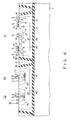
- Fig. 1 is a sectional view of a semiconductor device according to an embodiment of the present invention.
- lateral i nsulated g ate b ipolar t ransistor (IGBT) T1 as a high breakdown voltage element
- a plurality of bipolar transistors (Fig. 1 shows two transistors, i.e., pnp and npn transistors T2 and T3) as a plurality of low breakdown voltage elements used for a control circuit of transistor T1 are integrally formed.
- a plurality of p ⁇ -type Si layers 4a and 4b which are isolated from each other in island forms by SiO2 layers 3a and 3b are formed in Si substrate 4 on Si substrate 1.
- IGBT T1 is formed in one Si layer, i.e. layer 4a, whereas pnp and npn transistors T2 and T3 which are isolated from each other by pn junction isolation are formed in the other Si layer, i.e., layer 4b. This process will be described in detail in accordance with practical manufacturing steps.
- Figs. 2A to 2G show the manufacturing steps.
- two Si substrates 1 and 4 are prepared.
- One surface of each of Si substrates is mirror-polished.
- One substrate, i.e., Si substrate (first semiconductor substrate) 4 is a p ⁇ -type substrate for element formation, and has a resistivity of 70 to 100 ⁇ cm.
- SiO2 film 3a having a thickness of about 1 ⁇ m is formed on the surface of the resultant structure.
- the other substrate, i.e., Si substrate (second semiconductor substrate) 1 may be of p- or n-type, and has no limitation as to specific resistivity.
- Such two substrates 1 and 4 are bonded to each other by a silicon wafer direct-bonding technique. Then, a surface of substrate 4, which is opposite to the bonding surface, is polished to obtain p ⁇ -type Si layer 4 having a thickness of about 60 ⁇ m (Fig. 2B).
- SiO2 film 3a is used for element isolation. It has been confirmed from experiments performed by the present inventors that in order to reduce warpage of the resultant wafer, SiO2 film 3a must be formed on element formation substrate 4 in advance, and that bonding interface 2 must face the upper surface of SiO2 film 3a which is formed on element formation substrate 4 in advance.
- the steps of practical direct bonding are performed in the following manner.
- Substrates to be bonded are cleaned by an H2SO4-H2O2 mixture solution, HCl-H2O2 mixture solution, aqua regia, or the like.
- the substrates are cleaned by water for about ten minutes, and are dried by a spin dryer or the like.
- the substrates subjected to these processes are set in a clean atmosphere below, e.g., class 100, and their mirror-polished surfaces are bonded to each other in a state wherein substantially no contaminant is present therebetween. With this process, the two substrates are bonded to each other with a certain strength.
- heat-treatment can be performed in an oxygen, nitrogen, hydrogen, inert gas, steam, or a gas mixture thereof.
- cleaning was performed by an H2SO4-H2O2 mixture solution and an HCl-H2O2 mixture solution, and heat-treatment was performed a nitrogen atmosphere including a small amount of oxygen at 1,100°C for two hours.
- Si substrate 4 is lapped and polished to reduce the thickness.
- SiO2 film 31 is formed on the upper surface of Si substrate 4.
- Tapered isolation trench 32 is then formed by etching, e.g., anisotropic etching Si layer 4 to a depth reaching SiO2 film 3a using pattern 31a obtained by patterning SiO2 film 31 as a mask.
- Si layers 4a and 4b are isolated in the forms of islands (Fig. 2C). Boron is diffused in isolation trench 32 by diffusion so as to form p+-type layers 6b in the side walls of island Si layers 4a and 4b.
- p+-type layers 6b are integrated with p+-type layer 6a on the bottom of the isolation trench so as to constitute p+-type layer 6.
- SiO2 film 3b is formed in the side wall of each Si layer 4 by another thermal oxidation of the side wall. Then, SiO2 film 31 on the surface of Si layer 4b on the low breakdown voltage element side is patterned to form pattern 31a.
- Si layer 4 is etched by using pattern 31a as an etching mask to form recesses in the element region. Phosphorus or antimony is introduced in the recesses at a high concentration by diffusion to form n+-type layers 21a and 21b (Fig. 2D).
- SiO2 film 31b overhanging in the recesses need be theoretically removed when the epitaxial growth process in Fig. 2E is performed. However, if crystal growth is performed while SiO2 film 31b is locally left, a high-quality single crystal cannot be buried, and hence defects are often caused. In order to decrease the defects, SiO2 film 31b on the surface of Si layer 4b is preferably removed substantially entirely in crystal growth, as described above.
- Pnp transistor T2 and npn transistor T3 which are isolated from each other by a pn junction isolation are respectively formed in n ⁇ -type layers 22a and 22b buried in this manner.
- p-type layers 23 and 24 are formed in the surface region of n ⁇ -type 22a at a predetermined interval. Thereafter, collector, emitter, and base electrodes 27a, 28a, and 29a are formed. As a result, lateral type pnp transistor T2 having n ⁇ -type layer 22a serving as a base, and p-type layers 23 and 24 respectively serving as a collector and a emitter is formed.
- p-type layer 25 is formed in the surface region of n-type layer 22b by impurity diffusion.
- n-type layer 26 is formed in the surface region of p-type layer 25.
- collector, emitter, and base electrodes 27b, 28b, and 29b are formed to form vertical type npn transistor T3 having n ⁇ -type layer 22b as a collector, p-type layer 26 as a base, and n-type layer 26 as an emitter.
- p-type base layer 7 is formed in its peripheral portion, n-type source layer 8 is formed therein, n-type base layer 9 is formed in its central portion, and p-type drain layer 11 is formed therein by impurity diffusion.
- N ⁇ -type layer 10 serving as a guard ring is formed around n-type base layer 11 by impurity diffusion.
- Gate electrode 13 is formed on a region between n-type source layer 8 and n ⁇ -type layer 10 with gate insulating film 12 interposed therebetween.
- drain electrode 15 is formed on p-type drain layer 11
- source electrode 14 is formed on n-type source layer 8 and p-type base layer 7 so as to be simultaneously in contact with layers 8 and 7, thereby obtaining IGBT-T1 (Fig. 2G).
- high breakdown voltage IGBT-T1 processing a large current can be electrically isolated from low breakdown voltage transistors T2 and T3 operated by a small current with high reliability by a dielectric material.
- transistors T2 and T3 are isolated from each other by a pn junction isolation, an extra area for element isolation is not required. Therefore, a high integration density can be realized.
- two bipolar transistors are integrated as low breakdown voltage elements. The present invention, however, exhibits a noticeable effect in terms of integration density especially when a large number of low breakdown voltage elements are integrated.
- high-concentration p+-type layers 6 are formed on the oxide film interfaces of the bottom and side walls of the p ⁇ -type layers isolated in the forms of islands, thereby obtaining high reliability. More specifically, many defects are normally present in an oxide film interface. If a depletion layer extending from an element formed in the device reaches this interface, leak, a decrease in breakdown voltage, or the like may be caused. However, formation of p+-type layers 6 can prevent the depletion layer from reaching the interface.
- the high breakdown voltage elements preferably have a dielectric isolation structure.
- Fig. 3 shows an embodiment wherein transistors T2 and T3 in Fig. 1 are modified.
- n-type layers 33a and 33b respectively serving as a base layer and a collector layer of each of transistors T2 and T3 are formed by impurity diffusion.
- transistor characteristics are slightly inferior to those in the previous embodiment.
- the steps of forming the recesses, crystal growth, etching, and the like upon formation of the dielectric isolation structure are omitted, the overall steps can be greatly simplified, thereby decreasing the manufacturing cost.
- Fig. 4 shows an embodiment wherein lateral type MOSFET-T1 is used in place of IGBT-T1.
- n-type layer 9 is a drain layer, and drain electrode 15 is in direct contact therewith.
- MOSFET-T1 is not bipolar-operated but is unipolar-operated by ON/OFF control of a channel formed on its surface. In this embodiment, even when a plurality of identical lateral type MOSFETs are integrally formed, no specific element isolation is required between them.
- Fig. 5A shows an embodiment wherein vertical type MOSFET-T1 is used in place of IGBT-T1 in Fig. 1.
- substrate 1 has a double-layer structure consisting of n+- and n ⁇ -type layers 1a and 1b, and no SiO2 film is formed on bonding interface 2 in the region of MOSFET-T1.
- P-type base layer 52 is formed in a surface portion of n ⁇ -type layer 41a, n-type source layer 53 is formed therein, and n+-type layer 1a is formed as a drain, thereby forming vertical type MOSFET-T1.
- n+-type layer 1a can be replaced with p+-type layer.
- element T1 may be a MOS thyristor or IGBT.
- Fig. 5B shows an embodiment wherein npn transistor T1 is used in place of vertical type MOSFET-T1 in Fig. 5A.
- Npn transistor can be used in place of npn transistor.
- Fig. 5C shows an embodiment wherein GTO (gate turn-off thyristor) is used in place of vertical type MOSFET-T1 in Fig. 5A.
- Thyristor or MOSGTO can be used in place of GTO.
- Figs. 6 to 9 show embodiments wherein the arrangement of the bipolar transistor portions serving as low breakdown voltage elements is modified.
- p ⁇ -type layer 46, n-type well 61, and p-type well are formed by impurity diffusion, and a collector, a base, and an emitter are sequentially formed in the respective wells by impurity diffusion, thereby forming pnp and npn transistors T2 and T3.
- n- and p-type wells 61 and 62 are formed by diffusion, and hence lateral type pnp and npn transistors T2 and T3 are respectively formed therein.
- Fig. 6 p ⁇ -type layer 46, n-type well 61, and p-type well are formed by impurity diffusion, and a collector, a base, and an emitter are sequentially formed in the respective wells by impurity diffusion, thereby forming pnp and npn transistors T2 and T3.
- p-type layer 81 is formed in p ⁇ -type layer 4b independently of p+-type layer 6 prior to substrate bonding so as to reduce the resistance.
- lateral type transistor T2a and vertical type transistor T2b are simultaneously integrated as pnp transistors.
- Fig. 10 shows a structure of still another embodiment.
- space 91 is formed at a position of bonding interface 2 below the IGBT-T1 region serving as the high breakdown voltage element in Fig. 1.
- This structure is obtained by forming oxide film 3a to a sufficient thickness by a process prior to bonding, etching oxide film 3a in the high breakdown voltage element region, forming thin oxide film 3c in the etched portion again, and performing bonding. With this structure, a breakdown voltage in a bottom portion of the high breakdown voltage element side can be further increased.
- Fig. 11 is a sectional view of a semiconductor device in which low breakdown voltage elements are formed in two wells having V-shaped sectional areas.
- the method of forming a trench and burying a semiconductor layer therein, and the method of impurity diffusion are described as methods of forming wells isolated by pn junction isolation.
- the method of forming trenches described with reference to Figs. 2A to 2G is performed independently of the selective etching process for forming island Si layers by isolation. In this embodiment, however, trenches are formed in the wells simultaneously with the selective etching process for isolation of the island Si layers.
- the trenches for isolating/forming the island layers must reach the bottom portions while the trenches in the well regions must not reach the bottom portions.
- Such conditions can be obtained by applying anisotropic etching capable of obtaining a predetermined taper angle to selective etching so as to select the size of an etching window.
- Figs. 12A to 12G are sectional views showing the steps in manufacturing the semiconductor device in Fig. 11.
- the steps shown in Figs. 12A and 12B are the same as those in Figs. 2A and 2B.
- Si layer 4a on the high breakdown voltage element side and Si layer 4b on the low breakdown voltage element side are isolated from each other by forming isolation trench 32 by selective etching.
- trenches 32a and 32b are formed in the well regions on the low breakdown voltage element side (Fig. 12C).
- trench 32 of the isolation region can be caused to reach the bottom portion while trenches 32a and 32b in the well regions do not reach the bottom portions.
- n+-type layers 6c, 21a, and 21b are formed in the side walls of trenches 32, 32a, and 32b upon diffusion of phosphorus or arsenic by epitaxial diffusion (Fig. 12D).
- n ⁇ -type Si layer 22 is formed by removing an oxide film on the low breakdown voltage element side and forming an Si layer by epitaxial growth.
- polysilicon layer 5 is deposited on the high breakdown voltage element covered with the oxide film (Fig. 12E).
- n ⁇ -type layers 22a and 22b serving as wells are buried in the respective recesses in Si layer 4, and polysilicon layer 5 is buried in the isolation trench (Fig. 12F).
- IGBT-T1 is formed in Si layer 4a, and lateral type pnp transistor T2 and vertical type npn transistor T3 which are isolated from each other by a pn junction isolation are formed in Si layer 4b (Fig. 12G).
- Fig. 13 shows an embodiment wherein the structure in Fig. 11 is slightly modified.
- p+-type layers 6a are formed in the bottom portions of Si layers 4a and 4b
- n+-type layers 6c are formed on the side walls of the isolation trench simultaneously with formation of the n+-type layers on the side surfaces of the well region trenches.
- the p+-type layers are formed on the bottom and side walls of the island Si layers.
- Fig. 14 shows a structure of still another embodiment.
- n- and p-channel MOS transistors T4 and T5 constituting a CMOS circuit together with bipolar transistors T2 and T3 are formed in Si layer 4b on the low breakdown voltage element side.
- Bipolar transistors T2 and T3 are formed such that n ⁇ -type layer 22a formed by epitaxial growth is divided into a plurality of regions which are isolated from each other by a pn junction isolation, and transistors T2 and T3 are respectively formed in the regions.
- MOS transistors T4 and T5 are respectively formed in p- and n-type layers 22c and 22b formed by impurity diffusion.
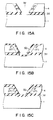
- a p+-type layer and an n+-type layer are formed on the inner surface of trench 32 shown in Figs. 2C and 12D, and SiO2 film 31, which has been used as the mask, is then removed by means or etching.
- SiO2 film 31 is removed away, SiO2 film 3a is inevitably etched away from the bottom of trench 32 as is shown in Fig. 15A.
- the side etching of SiO2 film 3a also proceeds. Thereafter, as is shown in Fig.
- SiO2 film 3b is formed on the inner surface of trench 32 by means of thermal oxidation.
- the thickness of SiO2 film 3a is determined by the breakdown voltage which is required of the interface between two Si substrates 1 and 4.
- the thickness of SiO2 film 3b is determined by the breakdown voltage which is required of the interface between island-shaped Si layers 4a and 4b.
- the breakdown voltage required of the interface between two Si substrates 1 and 4 is equal, in most cases, to that required of the interface between island-shaped Si layers 4a and 4b. Nonetheless, SiO2 film 3b is thinner than SiO2 film 3a since it is this SiO2 film 3b that isolates island-shaped Si layers 4a and 4b from each other.
- SiO2 film 3b is thinner than SiO2 film 3a, SiO2 film 3a is etched away from the bottom of trench 32 when SiO2 film 31 is etched away. Consequently, SiO2 film 3b formed on the bottom of trench 32 by thermal oxidation is thinner than SiO2 film 3a.
- the side-etched portion of SiO2 film 3a is particularly thin. SiO2 film 3b formed on the bottom of trench 32, which is thin, is electrically weak, and fails to have a breakdown voltage as high as is desired.
- SiO2 film 3b that is formed on the inner surface of trench 32, thicker than SiO2 film 3a formed between two Si substrates 1 and 4.
- SiO2 film 3b when SiO2 film 3b was made 1.5 ⁇ m thick, whereas SiO2 film 3a was made 1 ⁇ m thick, as is shown in Fig. 15C, the breakdown voltage of the interface between Si substrates 1 and 4 was as high as 700 to 800V.
- SiO2 film 3b was made 0.8 ⁇ m thick, while SiO2 film 3a was made 1 ⁇ m thick, the breakdown voltage of the interface between Si substrates 1 and 4 was only 500V to 600V.
- a dielectric isolation structure and a pn junction isolation structure are combined so that the integration density can be sufficiently increased while influences of noise and the like due to large current switching are effectively prevented.
Landscapes
- Element Separation (AREA)
- Metal-Oxide And Bipolar Metal-Oxide Semiconductor Integrated Circuits (AREA)
- Bipolar Integrated Circuits (AREA)
Abstract
Description
- The present invention relates to a semiconductor device having a high breakdown voltage element and a low breakdown voltage element formed in a single substrate and a method of manufacturing the same.
- Pn junction isolation and dielectric isolation are known as isolation techniques for semiconductor integrated circuits. Dielectric isolation is preferably employed to isolate a high breakdown voltage element used for large current switching from other elements so as to ensure reliable electrical isolation. When a high breakdown voltage element and a plurality of low breakdown voltage elements, such as bipolar transistors, constituting a control circuit for the high breakdown voltage element are integrated, dielectric isolation is preferably employed to prevent the low breakdown voltage elements from being electrically influenced by the high breakdown voltage element, e.g., prevent mixing of noise in the bipolar transistors due to large current switching. Generally, therefore, in a conventional integrated circuit using such dielectric isolation, a plurality of low breakdown voltage elements are respectively formed in different island regions isolated by a dielectric material in a substrate.
- A structure wherein all the elements are isolated from each other by a dielectric material in such a manner is not preferable in terms of integration density, because dielectric isolation requires a larger area than pn junction isolation.
- As described above, if the structure wherein all the elements are isolated by a dielectric material is employed in an integrated circuit having high and low breakdown voltage elements formed in a single substrate, an increase in integration density is limited.
- It is an object of the present invention to provide a semiconductor device in which a decrease in integration density due to isolation is prevented when high and low breakdown voltage elements are integrally formed on a single substrate.
- It is another object of the present invention to provide a method of manufacturing such a semiconductor device.
- According to the present invention, there is provided a semiconductor device comprising a semiconductor substrate, a pair of low breakdown voltage elements formed on the substrate so as to be adjacent to each other, and a high breakdown voltage element formed to be adjacent to one of the low breakdown voltage elements, wherein the pair of low breakdown voltage elements are isolated from each other by a pn junction and the one of the low breakdown voltage elements and the high breakdown voltage element are isolated from each other by a dielectric material.
- In the semiconductor device of the present invention, a composite substrate formed by directly bonding a first substrate serving as an element region a second substrate serving as a supporting member with an insulating film interposed therebetween can be used as the semiconductor substrate. In this case, of the composite substrate, the second substrate is of a first conductivity type having a low impurity concentration and is divided into a plurality of island regions which are isolated from each other by an isolating layer formed by burying a dielectric material in a trench. The high breakdown voltage element is formed in one island region, whereas the low breakdown voltage elements are formed in the other island region. The low breakdown voltage elements are isolated from each other by a pn junction.
- In addition, according to the present invention, there is provided a method of manufacturing a semiconductor substrate comprising the steps of mirror-polishing one surface of each of first semiconductor substrate of a first conductivity type and second semiconductor substrate, forming a first impurity region of the first conductivity type in the mirror-polished surface of the first semiconductor substrate, forming a first insulating film on at least one of a surface of the first impurity region and the mirror-polished surface of the second semiconductor substrate, forming a composite substrate by directly bonding the mirror-polished surface of the first semiconductor substrate to the mirror-polished surface of the second substrate, forming at least one groove by selectively etching a portion of the first semiconductor substrate of the composite substrate, forming second impurity regions by diffusing an impurity in side walls of a plurality of semiconductor layers which are isolated from each other by the groove, forming a second insulating film in surfaces of the second impurity regions, forming a high breakdown voltage element in one of the semiconductor layers, and forming a plurality of low breakdown voltage elements which are isolated from each other by a pn junction in the other one of the semiconductor layers.
- Furthermore, according to the present invention, there is provided a method of manufacturing a semiconductor substrate comprising the steps of mirror-polishing one surface of each of first semiconductor substrate of a first conductivity type and second semiconductor substrate, forming a first impurity region of the first conductivity type in the mirror-polished surface of the first semiconductor substrate, forming a first insulating film on at least one of a surface of the first impurity region and the mirror-polished surface of the second semiconductor substrate, forming a composite substrate by directly bonding the mirror-polished surface of the first semiconductor substrate to the mirror-polished surface of the second substrate, forming a first groove which reaches the insulating film and a plurality of second grooves which do not reach the first impurity region by selectively etching a portion of the first semiconductor substrate of the composite substrate, the first substrate being divided into a first semiconductor region and a second semiconductor region having the second trench which are isolated from each other by the first trench, forming second impurity region by diffusing an impurity in side walls of the first trench, forming a second insulating film on a surface of the second impurity region in the first groove, burying a dielectric material and semiconductor material layer in the first groove and the second grooves, respectively, forming a high breakdown voltage element in the first semiconductor region, and forming low breakdown voltage element which are isolated from each other by a pn junction in the semiconductor material layers.
- This invention can be more fully understood from the following detailed description when taken in conjunction with the accompanying drawings, in which:
- Fig. 1 is a sectional view of a semiconductor device according to one embodiment of the present invention;
- Figs. 2A to 2G are sectional views showing the steps in manufacturing the semiconductor device in Fig. 1;
- Fig. 3 is a sectional view of a semiconductor device in which a formation region of low breakdown voltage elements is formed by impurity diffusion;
- Fig. 4 is a sectional view of a semiconductor device in which a lateral MOSFET is used as a high breakdown voltage element;
- Fig. 5A to 5C are sectional views of semiconductor devices in which a vertical type device is used as a high breakdown voltage element;
- Figs. 6 to 9 are sectional views of semiconductor devices in which an arrangement of low breakdown voltage elements is variously changed;
- Fig. 10 is a sectional view of a semiconductor device in which a space is formed in a part of a bonding interface of a substrate;
- Fig. 11 is a sectional view of a semiconductor device in which a formation region of low breakdown voltage elements is formed simultaneously with formation of a trench for isolation;
- Figs. 12A to 12G are sectional views showing the steps in manufacturing the semiconductor device in Fig. 11;
- Figs. 13 and 14 are sectional views of semiconductor devices as modifications of the device in Fig. 11; and
- Figs. 15A to 15C are sectional views for explaining a modification of the present invention.
- Preferred embodiments will be described below with reference to the accompanying drawings.
- Fig. 1 is a sectional view of a semiconductor device according to an embodiment of the present invention. In this semiconductor device, lateral insulated gate bipolar transistor (IGBT) T1 as a high breakdown voltage element, and a plurality of bipolar transistors (Fig. 1 shows two transistors, i.e., pnp and npn transistors T2 and T3) as a plurality of low breakdown voltage elements used for a control circuit of transistor T1 are integrally formed. More specifically, a plurality of p⁻-
type Si layers SiO₂ layers Si substrate 4 onSi substrate 1. IGBT T1 is formed in one Si layer,i.e. layer 4a, whereas pnp and npn transistors T2 and T3 which are isolated from each other by pn junction isolation are formed in the other Si layer, i.e.,layer 4b. This process will be described in detail in accordance with practical manufacturing steps. - Figs. 2A to 2G show the manufacturing steps. First, two
Si substrates type layer 6a is formed in the mirror-polished surface ofsubstrate 4 by diffusing boron at a high concentration,SiO₂ film 3a having a thickness of about 1 µm is formed on the surface of the resultant structure. The other substrate, i.e., Si substrate (second semiconductor substrate) 1 may be of p- or n-type, and has no limitation as to specific resistivity. Such twosubstrates substrate 4, which is opposite to the bonding surface, is polished to obtain p⁻-type Si layer 4 having a thickness of about 60 µm (Fig. 2B).SiO₂ film 3a is used for element isolation. It has been confirmed from experiments performed by the present inventors that in order to reduce warpage of the resultant wafer,SiO₂ film 3a must be formed onelement formation substrate 4 in advance, and thatbonding interface 2 must face the upper surface ofSiO₂ film 3a which is formed onelement formation substrate 4 in advance. - The steps of practical direct bonding are performed in the following manner. Substrates to be bonded are cleaned by an H₂SO₄-H₂O₂ mixture solution, HCl-H₂O₂ mixture solution, aqua regia, or the like. Subsequently, the substrates are cleaned by water for about ten minutes, and are dried by a spin dryer or the like. The substrates subjected to these processes are set in a clean atmosphere below, e.g., class 100, and their mirror-polished surfaces are bonded to each other in a state wherein substantially no contaminant is present therebetween. With this process, the two substrates are bonded to each other with a certain strength. When the substrates bonded to each other in this manner are subjected to heat-treatment in a diffusion furnace or the like, bonding strength is increased, and the two substrates are completely bonded. An increase in bonding strength is observed at about 200°C or more, preferably at 800 to 1200°C. No special attention need be paid to the atmosphere for the heat-treatment process. For example, heat-treatment can be performed in an oxygen, nitrogen, hydrogen, inert gas, steam, or a gas mixture thereof. In the embodiment, cleaning was performed by an H₂SO₄-H₂O₂ mixture solution and an HCl-H₂O₂ mixture solution, and heat-treatment was performed a nitrogen atmosphere including a small amount of oxygen at 1,100°C for two hours.
- Subsequently, the surface of
Si substrate 4 is lapped and polished to reduce the thickness. And,SiO₂ film 31 is formed on the upper surface ofSi substrate 4. Taperedisolation trench 32 is then formed by etching, e.g., anisotropicetching Si layer 4 to a depth reachingSiO₂ film 3a usingpattern 31a obtained by patterningSiO₂ film 31 as a mask. With this process,Si layers isolation trench 32 by diffusion so as to form p⁺-type layers 6b in the side walls ofisland Si layers type layers 6b are integrated with p⁺-type layer 6a on the bottom of the isolation trench so as to constitute p⁺-type layer 6.SiO₂ film 3b is formed in the side wall of eachSi layer 4 by another thermal oxidation of the side wall. Then,SiO₂ film 31 on the surface ofSi layer 4b on the low breakdown voltage element side is patterned to formpattern 31a.Si layer 4 is etched by usingpattern 31a as an etching mask to form recesses in the element region. Phosphorus or antimony is introduced in the recesses at a high concentration by diffusion to form n⁺-type layers - Subsequently,
SiO₂ film 31b on the surface ofSi layer 4b in which the recesses are formed is removed, and epitaxial growth of Si is performed to form high-resistance n⁻-type layer 22. At the same time,polysilicon layer 5 is formed onSiO₂ film 31a on the isolation region covered withSiO₂ film 3b and on the other Si layer, i.e.,layer 4a (Fig. 2E). The growth layer surface is then lapped and polished so that the thickness ofsubstrate 4 is 20 to 100 µm, and n⁻-type layers polysilicon film 5 is buried in the isolation trench (Fig. 2F). Since n⁻-type layer 22 is buried only in the recesses and other portions thereof are removed, only portions ofSiO₂ film 31b overhanging in the recesses need be theoretically removed when the epitaxial growth process in Fig. 2E is performed. However, if crystal growth is performed whileSiO₂ film 31b is locally left, a high-quality single crystal cannot be buried, and hence defects are often caused. In order to decrease the defects,SiO₂ film 31b on the surface ofSi layer 4b is preferably removed substantially entirely in crystal growth, as described above. - Pnp transistor T2 and npn transistor T3 which are isolated from each other by a pn junction isolation are respectively formed in n⁻-
type layers - More specifically, p-
type layers type 22a at a predetermined interval. Thereafter, collector, emitter, andbase electrodes 27a, 28a, and 29a are formed. As a result, lateral type pnp transistor T2 having n⁻-type layer 22a serving as a base, and p-type layers - p-
type layer 25 is formed in the surface region of n-type layer 22b by impurity diffusion. In addition, n-type layer 26 is formed in the surface region of p-type layer 25. Then, collector, emitter, andbase electrodes type layer 22b as a collector, p-type layer 26 as a base, and n-type layer 26 as an emitter. - Subsequently, in p⁻-
type Si layer 4a, p-type base layer 7 is formed in its peripheral portion, n-type source layer 8 is formed therein, n-type base layer 9 is formed in its central portion, and p-type drain layer 11 is formed therein by impurity diffusion. N⁻-type layer 10 serving as a guard ring is formed around n-type base layer 11 by impurity diffusion.Gate electrode 13 is formed on a region between n-type source layer 8 and n⁻-type layer 10 withgate insulating film 12 interposed therebetween. Then, drainelectrode 15 is formed on p-type drain layer 11, andsource electrode 14 is formed on n-type source layer 8 and p-type base layer 7 so as to be simultaneously in contact withlayers - In the semiconductor device obtained in the above-described manner, high breakdown voltage IGBT-T1 processing a large current can be electrically isolated from low breakdown voltage transistors T2 and T3 operated by a small current with high reliability by a dielectric material. On the other hand, since transistors T2 and T3 are isolated from each other by a pn junction isolation, an extra area for element isolation is not required. Therefore, a high integration density can be realized. In the above embodiment, two bipolar transistors are integrated as low breakdown voltage elements. The present invention, however, exhibits a noticeable effect in terms of integration density especially when a large number of low breakdown voltage elements are integrated. Furthermore, in the above embodiment, high-concentration p⁺-
type layers 6 are formed on the oxide film interfaces of the bottom and side walls of the p⁻-type layers isolated in the forms of islands, thereby obtaining high reliability. More specifically, many defects are normally present in an oxide film interface. If a depletion layer extending from an element formed in the device reaches this interface, leak, a decrease in breakdown voltage, or the like may be caused. However, formation of p⁺-type layers 6 can prevent the depletion layer from reaching the interface. - Note that in the above embodiment, only one IGBT serving as a high breakdown voltage element is exemplified. However, a plurality of such elements may be integrally formed. In this case, the high breakdown voltage elements preferably have a dielectric isolation structure.
- The present invention is not limited to the above embodiment. Other embodiments will be described below. The same reference numerals in the drawings of the following embodiments denote the same parts as in the drawings of the previous embodiment, and a detailed description thereof will be omitted.
- Fig. 3 shows an embodiment wherein transistors T2 and T3 in Fig. 1 are modified. In this embodiment, n-
type layers 33a and 33b respectively serving as a base layer and a collector layer of each of transistors T2 and T3 are formed by impurity diffusion. - According to this embodiment, since a low-resistance n⁺-type buried layer such as shown in the previous embodiment is not formed, transistor characteristics are slightly inferior to those in the previous embodiment. However, since the steps of forming the recesses, crystal growth, etching, and the like upon formation of the dielectric isolation structure are omitted, the overall steps can be greatly simplified, thereby decreasing the manufacturing cost.
- Fig. 4 shows an embodiment wherein lateral type MOSFET-T1 is used in place of IGBT-T1. In this embodiment, n-
type layer 9, is a drain layer, and drainelectrode 15 is in direct contact therewith. Unlike IGBT-T1 in the embodiment of Fig. 1, MOSFET-T1 is not bipolar-operated but is unipolar-operated by ON/OFF control of a channel formed on its surface. In this embodiment, even when a plurality of identical lateral type MOSFETs are integrally formed, no specific element isolation is required between them. - Fig. 5A shows an embodiment wherein vertical type MOSFET-T1 is used in place of IGBT-T1 in Fig. 1. In this case,
substrate 1 has a double-layer structure consisting of n⁺- and n⁻-type layers 1a and 1b, and no SiO₂ film is formed onbonding interface 2 in the region of MOSFET-T1. P-type base layer 52 is formed in a surface portion of n⁻-type layer 41a, n-type source layer 53 is formed therein, and n⁺-type layer 1a is formed as a drain, thereby forming vertical type MOSFET-T1. - In Fig. 5A, n⁺-type layer 1a can be replaced with p⁺-type layer. In this case, element T1 may be a MOS thyristor or IGBT.
- Fig. 5B shows an embodiment wherein npn transistor T1 is used in place of vertical type MOSFET-T1 in Fig. 5A. Npn transistor can be used in place of npn transistor.
- Fig. 5C shows an embodiment wherein GTO (gate turn-off thyristor) is used in place of vertical type MOSFET-T1 in Fig. 5A. Thyristor or MOSGTO can be used in place of GTO.
- In these embodiments shown in Figs. 5A to 5C, the same effects as in the previous embodiment can be obtained.
- Figs. 6 to 9 show embodiments wherein the arrangement of the bipolar transistor portions serving as low breakdown voltage elements is modified. In Fig. 6, p⁻-type layer 46, n-
type well 61, and p-type well are formed by impurity diffusion, and a collector, a base, and an emitter are sequentially formed in the respective wells by impurity diffusion, thereby forming pnp and npn transistors T2 and T3. In Fig. 7, n- and p-type wells type layer 81 is formed in p⁻-type layer 4b independently of p⁺-type layer 6 prior to substrate bonding so as to reduce the resistance. In Fig. 9, lateral type transistor T2a and vertical type transistor T2b are simultaneously integrated as pnp transistors. - In the embodiments shown in Figs. 6 to 9, the same effects as in the previous embodiment can be obtained.
- Fig. 10 shows a structure of still another embodiment. In this embodiment,
space 91 is formed at a position ofbonding interface 2 below the IGBT-T1 region serving as the high breakdown voltage element in Fig. 1. This structure is obtained by formingoxide film 3a to a sufficient thickness by a process prior to bonding,etching oxide film 3a in the high breakdown voltage element region, forming thin oxide film 3c in the etched portion again, and performing bonding. With this structure, a breakdown voltage in a bottom portion of the high breakdown voltage element side can be further increased. - Fig. 11 is a sectional view of a semiconductor device in which low breakdown voltage elements are formed in two wells having V-shaped sectional areas. In the above-described embodiments, the method of forming a trench and burying a semiconductor layer therein, and the method of impurity diffusion are described as methods of forming wells isolated by pn junction isolation. The method of forming trenches described with reference to Figs. 2A to 2G is performed independently of the selective etching process for forming island Si layers by isolation. In this embodiment, however, trenches are formed in the wells simultaneously with the selective etching process for isolation of the island Si layers. The trenches for isolating/forming the island layers must reach the bottom portions while the trenches in the well regions must not reach the bottom portions. Such conditions can be obtained by applying anisotropic etching capable of obtaining a predetermined taper angle to selective etching so as to select the size of an etching window.
- Figs. 12A to 12G are sectional views showing the steps in manufacturing the semiconductor device in Fig. 11. The steps shown in Figs. 12A and 12B are the same as those in Figs. 2A and 2B.
Si layer 4a on the high breakdown voltage element side andSi layer 4b on the low breakdown voltage element side are isolated from each other by formingisolation trench 32 by selective etching. At the same time,trenches 32a and 32b are formed in the well regions on the low breakdown voltage element side (Fig. 12C). By selecting the size of a window of SiO₂ upon anisotropic etching,trench 32 of the isolation region can be caused to reach the bottom portion whiletrenches 32a and 32b in the well regions do not reach the bottom portions. Thereafter, n⁺-type layers trenches type Si layer 22 is formed by removing an oxide film on the low breakdown voltage element side and forming an Si layer by epitaxial growth. At the same time,polysilicon layer 5 is deposited on the high breakdown voltage element covered with the oxide film (Fig. 12E). Then, the grown layer is lapped, n⁻-type layers Si layer 4, andpolysilicon layer 5 is buried in the isolation trench (Fig. 12F). Thereafter, in an element forming process, IGBT-T1 is formed inSi layer 4a, and lateral type pnp transistor T2 and vertical type npn transistor T3 which are isolated from each other by a pn junction isolation are formed inSi layer 4b (Fig. 12G). - According to this embodiment, since isolation of the island Si layers and formation of the recesses in the well formation regions in the Si layers can be performed in a single etching process, the overall process can be simplified.
- Fig. 13 shows an embodiment wherein the structure in Fig. 11 is slightly modified. In Fig. 11, p⁺-
type layers 6a are formed in the bottom portions of Si layers 4a and 4b, and n⁺-type layers 6c are formed on the side walls of the isolation trench simultaneously with formation of the n⁺-type layers on the side surfaces of the well region trenches. In this embodiment, however, the p⁺-type layers are formed on the bottom and side walls of the island Si layers. - Fig. 14 shows a structure of still another embodiment. In this embodiment, n- and p-channel MOS transistors T4 and T5 constituting a CMOS circuit together with bipolar transistors T2 and T3 are formed in
Si layer 4b on the low breakdown voltage element side. Bipolar transistors T2 and T3 are formed such that n⁻-type layer 22a formed by epitaxial growth is divided into a plurality of regions which are isolated from each other by a pn junction isolation, and transistors T2 and T3 are respectively formed in the regions. MOS transistors T4 and T5 are respectively formed in p- and n-type layers 22c and 22b formed by impurity diffusion. - In the embodiment shown in Figs. 2A to 2G, and also the embodiment shown in Figs. 12A to 12G, a p⁺-type layer and an n⁺-type layer are formed on the inner surface of
trench 32 shown in Figs. 2C and 12D, andSiO₂ film 31, which has been used as the mask, is then removed by means or etching. WhenSiO₂ film 31 is removed away,SiO₂ film 3a is inevitably etched away from the bottom oftrench 32 as is shown in Fig. 15A. At the same time, the side etching ofSiO₂ film 3a also proceeds. Thereafter, as is shown in Fig. 15B,SiO₂ film 3b is formed on the inner surface oftrench 32 by means of thermal oxidation. The thickness ofSiO₂ film 3a is determined by the breakdown voltage which is required of the interface between twoSi substrates SiO₂ film 3b is determined by the breakdown voltage which is required of the interface between island-shaped Si layers 4a and 4b. The breakdown voltage required of the interface between twoSi substrates SiO₂ film 3b is thinner thanSiO₂ film 3a since it is thisSiO₂ film 3b that isolates island-shaped Si layers 4a and 4b from each other. - Since
SiO₂ film 3b is thinner thanSiO₂ film 3a,SiO₂ film 3a is etched away from the bottom oftrench 32 whenSiO₂ film 31 is etched away. Consequently,SiO₂ film 3b formed on the bottom oftrench 32 by thermal oxidation is thinner thanSiO₂ film 3a. The side-etched portion ofSiO₂ film 3a is particularly thin.SiO₂ film 3b formed on the bottom oftrench 32, which is thin, is electrically weak, and fails to have a breakdown voltage as high as is desired. - This problem can be solved by making
SiO₂ film 3b, that is formed on the inner surface oftrench 32, thicker thanSiO₂ film 3a formed between twoSi substrates SiO₂ film 3b was made 1.5 µm thick, whereasSiO₂ film 3a was made 1 µm thick, as is shown in Fig. 15C, the breakdown voltage of the interface betweenSi substrates SiO₂ film 3b was made 0.8 µm thick, whileSiO₂ film 3a was made 1 µm thick, the breakdown voltage of the interface betweenSi substrates - As has been described above, according to the present invention, in an integrated circuit in which high and low breakdown voltage elements coexist, a dielectric isolation structure and a pn junction isolation structure are combined so that the integration density can be sufficiently increased while influences of noise and the like due to large current switching are effectively prevented.
Claims (25)
Priority Applications (1)
| Application Number | Priority Date | Filing Date | Title |
|---|---|---|---|
| EP96104114A EP0721211B1 (en) | 1988-02-08 | 1989-02-06 | Semiconductor device |
Applications Claiming Priority (4)
| Application Number | Priority Date | Filing Date | Title |
|---|---|---|---|
| JP26787/88 | 1988-02-08 | ||
| JP2678788 | 1988-02-08 | ||
| JP24644188 | 1988-09-30 | ||
| JP246441/88 | 1988-09-30 |
Related Child Applications (2)
| Application Number | Title | Priority Date | Filing Date |
|---|---|---|---|
| EP96104114.2 Division-Into | 1989-02-06 | ||
| EP96104114A Division EP0721211B1 (en) | 1988-02-08 | 1989-02-06 | Semiconductor device |
Publications (2)
| Publication Number | Publication Date |
|---|---|
| EP0328331A2 true EP0328331A2 (en) | 1989-08-16 |
| EP0328331A3 EP0328331A3 (en) | 1991-03-20 |
Family
ID=26364616
Family Applications (2)
| Application Number | Title | Priority Date | Filing Date |
|---|---|---|---|
| EP96104114A Expired - Lifetime EP0721211B1 (en) | 1988-02-08 | 1989-02-06 | Semiconductor device |
| EP19890301137 Withdrawn EP0328331A3 (en) | 1988-02-08 | 1989-02-06 | Semiconductor device and method of manufacturing the same |
Family Applications Before (1)
| Application Number | Title | Priority Date | Filing Date |
|---|---|---|---|
| EP96104114A Expired - Lifetime EP0721211B1 (en) | 1988-02-08 | 1989-02-06 | Semiconductor device |
Country Status (5)
| Country | Link |
|---|---|
| US (1) | US5072287A (en) |
| EP (2) | EP0721211B1 (en) |
| JP (1) | JP2788269B2 (en) |
| KR (1) | KR920003442B1 (en) |
| DE (1) | DE68929504T2 (en) |
Cited By (13)
| Publication number | Priority date | Publication date | Assignee | Title |
|---|---|---|---|---|
| EP0398468A3 (en) * | 1989-05-16 | 1991-03-13 | Kabushiki Kaisha Toshiba | Dielectrically isolated substrate and semiconductor device using the same |
| EP0418737A1 (en) * | 1989-09-13 | 1991-03-27 | Kabushiki Kaisha Toshiba | Method of manufacturing a semiconductor substrate dielectric isolating structure |
| DE4042334A1 (en) * | 1990-02-27 | 1991-09-05 | Fraunhofer Ges Forschung | Mfg. insulated monocrystalline silicon island - implanting oxygen into highly doped monocrystalline region for forming insulated buried silicon di:oxide layer |
| DE4006158A1 (en) * | 1990-02-27 | 1991-09-12 | Fraunhofer Ges Forschung | METHOD FOR PRODUCING AN INSULATED, SINGLE-CRYSTAL SILICON ISLAND |
| WO1993003498A1 (en) * | 1991-08-08 | 1993-02-18 | Siemens Aktiengesellschaft | Integrated circuit with at least one insulated component |
| DE4127925A1 (en) * | 1990-02-27 | 1993-02-25 | Fraunhofer Ges Forschung | Mfr. of insulating, monocrystalline silicon@ island for microelectronic IC - by oxygen implanting doped monocrystalline silicon@ region, depositing epitaxial silicon@ layer, forming trench, forming mask on silicon@ wafer etc. |
| US5213993A (en) * | 1989-09-13 | 1993-05-25 | Kabushiki Kaisha Tobisha | Method of manufacturing semiconductor substrate dielectric isolating structure |
| US5496765A (en) * | 1993-06-23 | 1996-03-05 | Siemens Aktiengesellschaft | Method for manufacturing an insulating trench in a substrate for smart-power technologies |
| EP0813248A3 (en) * | 1996-06-12 | 2000-03-01 | Kabushiki Kaisha Toshiba | Dielectrically isolated IC merged with surge protection circuit and method for manufacturing the same |
| WO2004053993A1 (en) * | 2002-12-10 | 2004-06-24 | Power Electronics Design Centre | Power integrated circuits |
| WO2004064123A2 (en) | 2003-01-10 | 2004-07-29 | Fraunhofer-Gesellschaft zur Förderung der angewandten Forschung e.V | Method for the production of a semiconductor component |
| EP1191583A3 (en) * | 2000-09-08 | 2005-01-19 | Texas Instruments Incorporated | Low voltage transistor |
| EP1969634A4 (en) * | 2006-01-05 | 2011-04-20 | Int Rectifier Corp | VERTICAL DMOS DEVICE IN AN INTEGRATED CIRCUIT |
Families Citing this family (55)
| Publication number | Priority date | Publication date | Assignee | Title |
|---|---|---|---|---|
| US5294825A (en) * | 1987-02-26 | 1994-03-15 | Kabushiki Kaisha Toshiba | High breakdown voltage semiconductor device |
| US5592014A (en) * | 1987-02-26 | 1997-01-07 | Kabushiki Kaisha Toshiba | High breakdown voltage semiconductor device |
| US5241211A (en) * | 1989-12-20 | 1993-08-31 | Nec Corporation | Semiconductor device |
| US5294559A (en) * | 1990-07-30 | 1994-03-15 | Texas Instruments Incorporated | Method of forming a vertical transistor |
| JP3111500B2 (en) * | 1991-05-09 | 2000-11-20 | 富士電機株式会社 | Manufacturing method of dielectric isolation wafer |
| US5227653A (en) * | 1991-08-07 | 1993-07-13 | North American Philips Corp. | Lateral trench-gate bipolar transistors |
| EP0534632B1 (en) * | 1991-09-24 | 2002-01-16 | Matsushita Electronics Corporation, Ltd. | Semiconductor integrated circuit device and method of fabricating the same |
| DE69231803T2 (en) * | 1991-10-14 | 2001-12-06 | Denso Corp., Kariya | Method of manufacturing a semiconductor device |
| US5389569A (en) * | 1992-03-03 | 1995-02-14 | Motorola, Inc. | Vertical and lateral isolation for a semiconductor device |
| JPH05251292A (en) * | 1992-03-06 | 1993-09-28 | Nec Corp | Manufacture of semiconductor device |
| US5436173A (en) * | 1993-01-04 | 1995-07-25 | Texas Instruments Incorporated | Method for forming a semiconductor on insulator device |
| US5892264A (en) * | 1993-10-04 | 1999-04-06 | Harris Corporation | High frequency analog transistors, method of fabrication and circuit implementation |
| JP3252569B2 (en) * | 1993-11-09 | 2002-02-04 | 株式会社デンソー | Insulating separation substrate, semiconductor device using the same, and method of manufacturing the same |
| JP3344598B2 (en) * | 1993-11-25 | 2002-11-11 | 株式会社デンソー | Semiconductor nonvolatile memory device |
| JP3255547B2 (en) * | 1994-03-09 | 2002-02-12 | 株式会社東芝 | Thyristor with insulated gate |
| US5841197A (en) * | 1994-11-18 | 1998-11-24 | Adamic, Jr.; Fred W. | Inverted dielectric isolation process |
| US6124179A (en) * | 1996-09-05 | 2000-09-26 | Adamic, Jr.; Fred W. | Inverted dielectric isolation process |
| US6411155B2 (en) | 1994-12-30 | 2002-06-25 | Sgs-Thomson Microelectronics S.A. | Power integrated circuit |
| FR2729008B1 (en) * | 1994-12-30 | 1997-03-21 | Sgs Thomson Microelectronics | INTEGRATED POWER CIRCUIT |
| JP3435930B2 (en) * | 1995-09-28 | 2003-08-11 | 株式会社デンソー | Semiconductor device and manufacturing method thereof |
| US6831331B2 (en) | 1995-11-15 | 2004-12-14 | Denso Corporation | Power MOS transistor for absorbing surge current |
| US6242787B1 (en) | 1995-11-15 | 2001-06-05 | Denso Corporation | Semiconductor device and manufacturing method thereof |
| US5874767A (en) * | 1996-05-14 | 1999-02-23 | Mitsubishi Denki Kabushiki Kaisha | Semiconductor device including a lateral power device |
| US5929368A (en) * | 1996-12-09 | 1999-07-27 | The Ensign-Bickford Company | Hybrid electronic detonator delay circuit assembly |
| US5889310A (en) * | 1997-04-21 | 1999-03-30 | Mitsubishi Denki Kabushiki Kaisha | Semiconductor device with high breakdown voltage island region |
| US6133607A (en) * | 1997-05-22 | 2000-10-17 | Kabushiki Kaisha Toshiba | Semiconductor device |
| KR100664333B1 (en) * | 1997-10-28 | 2007-01-02 | 코닌클리케 필립스 일렉트로닉스 엔.브이. | Semiconductor devices |
| DE69838422D1 (en) * | 1998-10-23 | 2007-10-25 | St Microelectronics Srl | High-voltage resistance structure integrated on a semiconductor substrate |
| JP4206543B2 (en) | 1999-02-02 | 2009-01-14 | 株式会社デンソー | Semiconductor device |
| EP1028468A1 (en) * | 1999-02-09 | 2000-08-16 | STMicroelectronics S.r.l. | Biasing circuit for isolation region in integrated power circuit |
| TW502458B (en) * | 1999-06-09 | 2002-09-11 | Toshiba Corp | Bonding type semiconductor substrate, semiconductor light emission element and manufacturing method thereof |
| US6879023B1 (en) * | 2000-03-22 | 2005-04-12 | Broadcom Corporation | Seal ring for integrated circuits |
| US6768183B2 (en) * | 2001-04-20 | 2004-07-27 | Denso Corporation | Semiconductor device having bipolar transistors |
| US6670255B2 (en) * | 2001-09-27 | 2003-12-30 | International Business Machines Corporation | Method of fabricating lateral diodes and bipolar transistors |
| JP2003264244A (en) * | 2002-03-08 | 2003-09-19 | Seiko Epson Corp | Semiconductor device and method of manufacturing the same |
| DE102004028474B4 (en) * | 2004-06-11 | 2009-04-09 | X-Fab Semiconductor Foundries Ag | Integrated component in a SOI disk |
| KR100582374B1 (en) * | 2004-09-08 | 2006-05-22 | 매그나칩 반도체 유한회사 | High voltage transistor and method of manufacturing the same |
| DE102004053077B4 (en) * | 2004-11-03 | 2006-11-02 | X-Fab Semiconductor Foundries Ag | Vertical PIN photodiode and manufacturing process, compatible with a conventional CMOS process |
| US20070228505A1 (en) * | 2006-04-04 | 2007-10-04 | Mazzola Michael S | Junction barrier schottky rectifiers having epitaxially grown p+-n junctions and methods of making |
| JP4793078B2 (en) * | 2006-04-25 | 2011-10-12 | 株式会社デンソー | Semiconductor device |
| JP5036234B2 (en) | 2006-07-07 | 2012-09-26 | 三菱電機株式会社 | Semiconductor device |
| US20080128762A1 (en) * | 2006-10-31 | 2008-06-05 | Vora Madhukar B | Junction isolated poly-silicon gate JFET |
| US7700405B2 (en) * | 2007-02-28 | 2010-04-20 | Freescale Semiconductor, Inc. | Microelectronic assembly with improved isolation voltage performance and a method for forming the same |
| US8168466B2 (en) * | 2007-06-01 | 2012-05-01 | Semiconductor Components Industries, Llc | Schottky diode and method therefor |
| JP5479671B2 (en) * | 2007-09-10 | 2014-04-23 | ローム株式会社 | Semiconductor device |
| DE102008028452B4 (en) | 2008-06-14 | 2012-10-25 | X-Fab Semiconductor Foundries Ag | Power transistor for high voltages in SOI technology |
| DE102008049732B4 (en) | 2008-09-30 | 2011-06-09 | Amd Fab 36 Limited Liability Company & Co. Kg | Semiconductor device with buried polysilicon resistor and method for its production |
| JP5446388B2 (en) * | 2009-03-31 | 2014-03-19 | サンケン電気株式会社 | Method for manufacturing integrated semiconductor device |
| KR101148335B1 (en) * | 2009-07-23 | 2012-05-21 | 삼성전기주식회사 | Photoelectric multiplier using semiconductor and cell structure thereof |
| KR101084940B1 (en) * | 2009-09-28 | 2011-11-17 | 삼성전기주식회사 | Silicon photoelectric multiplier |
| JP5434961B2 (en) | 2010-08-04 | 2014-03-05 | 株式会社デンソー | Semiconductor device having lateral diode |
| US8476684B2 (en) * | 2010-09-29 | 2013-07-02 | Analog Devices, Inc. | Field effect transistors having improved breakdown voltages and methods of forming the same |
| JP5711646B2 (en) * | 2010-11-16 | 2015-05-07 | 株式会社豊田中央研究所 | diode |
| CN104282552A (en) * | 2013-07-03 | 2015-01-14 | 无锡华润上华半导体有限公司 | Method for manufacturing IGBT |
| JP6155911B2 (en) | 2013-07-04 | 2017-07-05 | 三菱電機株式会社 | Semiconductor device |
Family Cites Families (25)
| Publication number | Priority date | Publication date | Assignee | Title |
|---|---|---|---|---|
| US3370995A (en) * | 1965-08-02 | 1968-02-27 | Texas Instruments Inc | Method for fabricating electrically isolated semiconductor devices in integrated circuits |
| FR1527898A (en) * | 1967-03-16 | 1968-06-07 | Radiotechnique Coprim Rtc | Arrangement of semiconductor devices carried by a common support and its manufacturing method |
| JPS4944555A (en) * | 1972-09-04 | 1974-04-26 | ||
| US3858062A (en) * | 1973-02-15 | 1974-12-31 | Motorola Inc | Solid state current divider |
| JPS5423388A (en) * | 1977-07-22 | 1979-02-21 | Hitachi Ltd | Semiconductor integrated-circuit device and its manufacture |
| JPS5951743B2 (en) * | 1978-11-08 | 1984-12-15 | 株式会社日立製作所 | semiconductor integrated device |
| JPS6042844A (en) * | 1983-08-18 | 1985-03-07 | Nec Corp | Semiconductor integrated circuit |
| JPS6051700A (en) * | 1983-08-31 | 1985-03-23 | Toshiba Corp | Bonding method of silicon crystalline body |
| JPS6058633A (en) * | 1983-09-12 | 1985-04-04 | Hitachi Ltd | Semiconductor integrated circuit device |
| EP0161740B1 (en) * | 1984-05-09 | 1991-06-12 | Kabushiki Kaisha Toshiba | Method of manufacturing semiconductor substrate |
| JPS6134971A (en) * | 1984-07-25 | 1986-02-19 | Matsushita Electric Works Ltd | Semiconductor device |
| JPS6159852A (en) * | 1984-08-31 | 1986-03-27 | Toshiba Corp | Manufacture of semiconductor device |
| FR2571544B1 (en) * | 1984-10-05 | 1987-07-31 | Haond Michel | PROCESS FOR MANUFACTURING ELECTRICALLY ISOLATED MONOCRYSTALLINE SILICON ISLANDS FROM EACH OTHER |
| JPH0770474B2 (en) * | 1985-02-08 | 1995-07-31 | 株式会社東芝 | Method for manufacturing compound semiconductor device |
| JPH0770476B2 (en) * | 1985-02-08 | 1995-07-31 | 株式会社東芝 | Method for manufacturing semiconductor device |
| JPS61184843A (en) * | 1985-02-13 | 1986-08-18 | Toshiba Corp | Composite semiconductor device and manufacture thereof |
| CA1251514A (en) * | 1985-02-20 | 1989-03-21 | Tadashi Sakai | Ion selective field effect transistor sensor |
| JPS61196576A (en) * | 1985-02-26 | 1986-08-30 | Nissan Motor Co Ltd | Semiconductor device |
| JPS6248039A (en) * | 1985-08-28 | 1987-03-02 | Nec Corp | Dielectric isolated integrated circuit |
| JPH0671067B2 (en) * | 1985-11-20 | 1994-09-07 | 株式会社日立製作所 | Semiconductor device |
| JPS6276646A (en) * | 1985-09-30 | 1987-04-08 | Toshiba Corp | Manufacture of semiconductor device |
| JPS6276645A (en) * | 1985-09-30 | 1987-04-08 | Toshiba Corp | Structure of composite semiconductor crystal |
| US4751561A (en) * | 1986-04-29 | 1988-06-14 | Rca Corporation | Dielectrically isolated PMOS, NMOS, PNP and NPN transistors on a silicon wafer |
| US4897362A (en) * | 1987-09-02 | 1990-01-30 | Harris Corporation | Double epitaxial method of fabricating semiconductor devices on bonded wafers |
| JPH01179342A (en) * | 1988-01-05 | 1989-07-17 | Toshiba Corp | Composite semiconductor crystal |
-
1988
- 1988-12-28 JP JP63333588A patent/JP2788269B2/en not_active Expired - Lifetime
-
1989
- 1989-02-06 EP EP96104114A patent/EP0721211B1/en not_active Expired - Lifetime
- 1989-02-06 EP EP19890301137 patent/EP0328331A3/en not_active Withdrawn
- 1989-02-06 DE DE68929504T patent/DE68929504T2/en not_active Expired - Lifetime
- 1989-02-08 KR KR1019890001412A patent/KR920003442B1/en not_active Expired
-
1991
- 1991-01-22 US US07/643,087 patent/US5072287A/en not_active Expired - Lifetime
Cited By (15)
| Publication number | Priority date | Publication date | Assignee | Title |
|---|---|---|---|---|
| EP0398468A3 (en) * | 1989-05-16 | 1991-03-13 | Kabushiki Kaisha Toshiba | Dielectrically isolated substrate and semiconductor device using the same |
| EP0418737A1 (en) * | 1989-09-13 | 1991-03-27 | Kabushiki Kaisha Toshiba | Method of manufacturing a semiconductor substrate dielectric isolating structure |
| US5213993A (en) * | 1989-09-13 | 1993-05-25 | Kabushiki Kaisha Tobisha | Method of manufacturing semiconductor substrate dielectric isolating structure |
| DE4006158A1 (en) * | 1990-02-27 | 1991-09-12 | Fraunhofer Ges Forschung | METHOD FOR PRODUCING AN INSULATED, SINGLE-CRYSTAL SILICON ISLAND |
| DE4127925A1 (en) * | 1990-02-27 | 1993-02-25 | Fraunhofer Ges Forschung | Mfr. of insulating, monocrystalline silicon@ island for microelectronic IC - by oxygen implanting doped monocrystalline silicon@ region, depositing epitaxial silicon@ layer, forming trench, forming mask on silicon@ wafer etc. |
| DE4042334A1 (en) * | 1990-02-27 | 1991-09-05 | Fraunhofer Ges Forschung | Mfg. insulated monocrystalline silicon island - implanting oxygen into highly doped monocrystalline region for forming insulated buried silicon di:oxide layer |
| WO1993003498A1 (en) * | 1991-08-08 | 1993-02-18 | Siemens Aktiengesellschaft | Integrated circuit with at least one insulated component |
| US5496765A (en) * | 1993-06-23 | 1996-03-05 | Siemens Aktiengesellschaft | Method for manufacturing an insulating trench in a substrate for smart-power technologies |
| EP0813248A3 (en) * | 1996-06-12 | 2000-03-01 | Kabushiki Kaisha Toshiba | Dielectrically isolated IC merged with surge protection circuit and method for manufacturing the same |
| EP1191583A3 (en) * | 2000-09-08 | 2005-01-19 | Texas Instruments Incorporated | Low voltage transistor |
| WO2004053993A1 (en) * | 2002-12-10 | 2004-06-24 | Power Electronics Design Centre | Power integrated circuits |
| WO2004064123A2 (en) | 2003-01-10 | 2004-07-29 | Fraunhofer-Gesellschaft zur Förderung der angewandten Forschung e.V | Method for the production of a semiconductor component |
| WO2004064123A3 (en) * | 2003-01-10 | 2004-09-10 | Fraunhofer Ges Forschung | Method for the production of a semiconductor component |
| US7719077B2 (en) | 2003-01-10 | 2010-05-18 | Fraunhofer-Gesellschaft zur Förderung der angewandten Forschung e.V. | Method for the production of a semiconductor component |
| EP1969634A4 (en) * | 2006-01-05 | 2011-04-20 | Int Rectifier Corp | VERTICAL DMOS DEVICE IN AN INTEGRATED CIRCUIT |
Also Published As
| Publication number | Publication date |
|---|---|
| EP0721211A2 (en) | 1996-07-10 |
| EP0721211A3 (en) | 1996-12-27 |
| DE68929504T2 (en) | 2004-09-23 |
| DE68929504D1 (en) | 2004-01-15 |
| JP2788269B2 (en) | 1998-08-20 |
| KR890013770A (en) | 1989-09-26 |
| EP0328331A3 (en) | 1991-03-20 |
| KR920003442B1 (en) | 1992-05-01 |
| EP0721211B1 (en) | 2003-12-03 |
| JPH02168646A (en) | 1990-06-28 |
| US5072287A (en) | 1991-12-10 |
Similar Documents
| Publication | Publication Date | Title |
|---|---|---|
| EP0328331A2 (en) | Semiconductor device and method of manufacturing the same | |
| US5049968A (en) | Dielectrically isolated substrate and semiconductor device using the same | |
| US5332920A (en) | Dielectrically isolated high and low voltage substrate regions | |
| US5512774A (en) | Dielectrically isolated substrate and semiconductor device using the same | |
| US5304821A (en) | MOS-gate-turnoff thyristor | |
| US6559505B1 (en) | Power integrated circuit with vertical current flow and related manufacturing process | |
| US4892837A (en) | Method for manufacturing semiconductor integrated circuit device | |
| US4985745A (en) | Substrate structure for composite semiconductor device | |
| US4881107A (en) | IC device having a vertical MOSFET and an auxiliary component | |
| US4570330A (en) | Method of producing isolated regions for an integrated circuit substrate | |
| KR100191789B1 (en) | Bipolar transistor , semiconductor device having bipolar transistor and manufacturing method of the same | |
| US6010950A (en) | Method of manufacturing semiconductor bonded substrate | |
| JP2979554B2 (en) | Method for manufacturing semiconductor device | |
| KR100366896B1 (en) | Semiconductor device | |
| JP2000068372A (en) | Semiconductor device and manufacturing method thereof | |
| US3959812A (en) | High-voltage semiconductor integrated circuit | |
| JPH09129763A (en) | Semiconductor integrated circuit | |
| JPS6394667A (en) | Semiconductor integrated circuit | |
| JP2752655B2 (en) | Bipolar integrated circuit device | |
| JPS6140140B2 (en) | ||
| JPH0997853A (en) | Semiconductor integrated circuit and its manufacturing method | |
| JPS63140561A (en) | Manufacturing method of semiconductor integrated circuit | |
| JPH0346335A (en) | Bipolar-type semiconductor integrated circuit | |
| JPS6156624B2 (en) | ||
| JPH0697275A (en) | Semiconductor device |
Legal Events
| Date | Code | Title | Description |
|---|---|---|---|
| PUAI | Public reference made under article 153(3) epc to a published international application that has entered the european phase |
Free format text: ORIGINAL CODE: 0009012 |
|
| 17P | Request for examination filed |
Effective date: 19890216 |
|
| AK | Designated contracting states |
Kind code of ref document: A2 Designated state(s): DE FR IT |
|
| PUAL | Search report despatched |
Free format text: ORIGINAL CODE: 0009013 |
|
| AK | Designated contracting states |
Kind code of ref document: A3 Designated state(s): DE FR IT |
|
| 17Q | First examination report despatched |
Effective date: 19910827 |
|
| STAA | Information on the status of an ep patent application or granted ep patent |
Free format text: STATUS: THE APPLICATION IS DEEMED TO BE WITHDRAWN |
|
| 18D | Application deemed to be withdrawn |
Effective date: 19981105 |