EP0326053B1 - Datensicherungsverfahren für einen programmierbaren Speicher - Google Patents
Datensicherungsverfahren für einen programmierbaren Speicher Download PDFInfo
- Publication number
- EP0326053B1 EP0326053B1 EP89101077A EP89101077A EP0326053B1 EP 0326053 B1 EP0326053 B1 EP 0326053B1 EP 89101077 A EP89101077 A EP 89101077A EP 89101077 A EP89101077 A EP 89101077A EP 0326053 B1 EP0326053 B1 EP 0326053B1
- Authority
- EP
- European Patent Office
- Prior art keywords
- address
- data storage
- register
- memory
- protect
- Prior art date
- Legal status (The legal status is an assumption and is not a legal conclusion. Google has not performed a legal analysis and makes no representation as to the accuracy of the status listed.)
- Expired - Lifetime
Links
Images


Classifications
-
- G—PHYSICS
- G11—INFORMATION STORAGE
- G11C—STATIC STORES
- G11C11/00—Digital stores characterised by the use of particular electric or magnetic storage elements; Storage elements therefor
- G11C11/21—Digital stores characterised by the use of particular electric or magnetic storage elements; Storage elements therefor using electric elements
- G11C11/34—Digital stores characterised by the use of particular electric or magnetic storage elements; Storage elements therefor using electric elements using semiconductor devices
-
- G—PHYSICS
- G06—COMPUTING OR CALCULATING; COUNTING
- G06F—ELECTRIC DIGITAL DATA PROCESSING
- G06F12/00—Accessing, addressing or allocating within memory systems or architectures
- G06F12/14—Protection against unauthorised use of memory or access to memory
- G06F12/1416—Protection against unauthorised use of memory or access to memory by checking the object accessibility, e.g. type of access defined by the memory independently of subject rights
- G06F12/1425—Protection against unauthorised use of memory or access to memory by checking the object accessibility, e.g. type of access defined by the memory independently of subject rights the protection being physical, e.g. cell, word, block
- G06F12/1441—Protection against unauthorised use of memory or access to memory by checking the object accessibility, e.g. type of access defined by the memory independently of subject rights the protection being physical, e.g. cell, word, block for a range
Definitions
- the present invention relates to integrated circuit memory devices and, in particular, to an integrated, non-volatile, reconfigurable data protection scheme for an electrically erasable programmable read only memory (EEPROM) device.
- EEPROM electrically erasable programmable read only memory
- a memory comprises an array of locations for storing information items, generally referred to as "words", in the form of a plurality of digital bits, i.e. 1s or 0s.
- words information items
- Each storage location in the array has an associated address which defines its position in the memory array. Access to that location for the purpose of writing in or reading out an information word is gained by specifying the proper address together with an instruction that identifies the operation to be performed at the specified address.
- Protection schemes are available for external bulk memory, such electrostatic system memory or magnetic core memory, of the type usually associated with data processing systems.
- U.S. Pat. No. 3,264,615 issued to R. P. Case et al. on August 2, 1966, discloses a data processing system having an addressable bulk memory, a register for holding a memory address field which consists of a plurality of address bits that are common to a group of addresses, and comparison circuitry for comparing the address field held in the register with memory addresses sought to be accessed. The comparison determines whether the address sought to be accessed contains the pattern specified by the field. Control circuitry signals a violation of a protected area in response to a predetermined result of the comparison. The control circuit can cause either an equal or an unequal comparison result to signal a violation.
- the address field may specify either a protected area or an unprotected area separating non-contiguous protected areas. Variation in the size of the protected area is accomplished by varying the number of address bits in the field which must be compared. A count register holding a value identifying the number of bits to be compared controls this process. The field register, count register and the circuitry for determining which comparison result will signal violation of a protected area are all subject to program control so that their contents and status may be altered at will.
- the system is provided with registers for storing upper and lower memory limits for data to be read, data to be written and instructions to be fetched for execution.
- Comparison circuitry responds to a request from memory for comparing each memory request with the limits stored in the register file. The request for memory access is enabled only if the comparison indicates that the access is within the specified limits.
- U.S. Pat. 3,742,458 issued to Inoue et al. on June 26, 1973, discloses an apparatus for flexible protection against overwriting and destruction of the contents of selected portions of memory.
- Each memory unit is assigned a unique memory address number which serves to identify the memory unit and instructions to write data into the memory.
- the addresses are segregated into ranges of numbers defining separate memory portions to be protected, with the numbers at the boundaries of the ranges being entered into registers which can be reset to flexibly determine the protected ranges.
- the memory device is separated into three different portions: one permitting free writing access to the memory units, one withholding all writing access to the memory units, and one being conditioned to grant or withhold writing access according to the setting of a device, such as a flip-flop, which can be arranged for manual or programmable control.
- a device such as a flip-flop, which can be arranged for manual or programmable control.
- the associated address number is entered into a register and compared by means of digital comparators with the range boundary numbers in their registers.
- a gate then grants or withholds access to the memory unit in accordance with the comparison, thereby controlling the insertion of data into each memory unit and providing protection to selected portions of the memory device.
- ROMs Read-Only-Memories
- UVEPROMs Ultraviolet Erasable Programmable ROMs
- EEPROM Electrically Erasable ROM
- the document FR-A-2 580 851 discloses an electrically erasable programmable read-only memory as set forth in the preamble of patent claim 1. This document further teaches means to select whether or not banks of the memory array are or are not write-protected.
- the document US-A-4,298,934 discloses a microprocessor system wherein the storage registers of a selected part of the volatile memory are protected from any write operation.
- the system includes a volatile protect register which stores the address of a preselected storage register such that all storage registers having addresses smaller than the address of the preselected storage register are write-protected.
- the document EP-A 0 218 523 discloses a volatile memory wherein the storage registers of a selected part of the memory are write-protected. It includes two protect registers, a start address register, and a stop address register, both storing boundary addresses between which writing is permitted while the other storage registers are protected. At the end of the description, it is mentioned, without indicating any advantage, that the protect register may be an EPROM circuit.
- the memory device according to the invention is indicated in claim 1.
- the number of protected registers within the memory array is user-controlled and the range of protected registers can be varied from the last register only to all registers being fully protected against data modifications.
- N registers where N is less than or equal to the total number of registers in the array, can be protected against data modification by programming the address of the first register to be protected into a special, integrated memory protect register. All memory registers having addresses equal to or greater than the address specified in the memory protect register are then protected from any write operation. This address can be "locked" into the memory protect register to provide permanent data security to all protected registers. That is, a portion of the memory array can be converted to ROM.
- the memory protect register is a non-volatile register comprising electrically erasable elements.
- Fig. 1 is a block diagram illustrating the basic elements of a 4K-bit EEPROM array which utilizes a memory data protection scheme in accordance with the present invention.
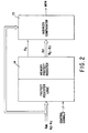
- Fig. 2 is a block diagram illustrating a memory data protection scheme in accordance with the present invention.
- Fig. 3 is a circuit diagram illustrating an embodiment of memory data protection circuitry in accordance with the present invention.
- Fig. 4 is a circuit diagram illustrating in detail an embodiment of the protect register logic and memory protect register circuit blocks 24 and 26, respectively, shown in Fig. 3.
- Fig. 5A is a cross-sectional view illustrating a portion of the nonvolatile memory cell utilized in the latch 26 as shown in Fig. 4.
- Fig. 5B is a cross-sectional view illustrating a second portion of the nonvolatile memory cell utilized in the latch 26 shown in Fig. 4.
- Fig. 6 is a block diagram illustrating use of the latch 26 shown in Fig. 4 in accordance with the present invention.
- Fig. 1 shows the basic elements of an electrically erasable programmable read only memory (EEPROM) device 10.
- the device 10 includes an EEPROM array 12 which is divided into 256 data storage registers of 16 bits each.
- Each of the storage registers in the array 12 has an address associated with it; the addresses define the storage registers sequentially from an initial register (i.e. R 1 ) to a final register (i.e. R 256 ).
- N registers (N ⁇ 256) in the array 12 can be protected against data modification by programming into a special on-chip, memory protect register 14 the address of the first register in the memory array 12 to be protected. Thereafter, all attempts to alter data in a storage register within the array 12 whose address is equal to or greater than the address stored in the memory protect register 14 will be ignored.
- data is written into the memory array 12 by serially clocking a WRITE instruction into an instruction register 16 and then clocking 16 bits of data to be written into the address specified in the WRITE instruction into a data shift register 18. After the 16 bits of data have been clocked into data shift register 18, this data is transferred in parallel to the specified storage register in array 12 via sense amplifiers 20 in a single, self-timed, 7.5 ms WRITE cycle.
- a READ instruction loads the address of the first memory register to be read from the instruction register 16 into an 8-bit address register 22.
- the data from the accessed storage register within the array 12 is then transferred in parallel to the data shift register 18 and then clocked out serially to the Data-Out pin DO.
- This register stores the address of the first register in the array 12 to be protected. All registers whose addresses are equal to or greater than the address specified in the protect register 12 will be protected from any WRITE operation. This address can also be "locked" into the protect register to provide permanent data security to all the protected registers, that is, converting a portion of the EEPROM array 12 into ROM.
- Fig. 2 provides a simple block diagram of the memory protection scheme of the present invention.
- "Ap” is the address stored in the memory protect register 14.
- the protect register 14 is a non-volatile register comprising electrically-erasable elements.
- An address comparator 13 compares the address stored in the protect register 14 with the present input address Ain.
- a Write Enable signal WEN for array 12 goes high enabling the appropriate address decoder 15 (see Fig. 1) if and only if Ap > Ain.
- PRCLR Protected Register Clear
- the protect register 14 is programmed with the address of the first register in the array 12, which converts the entire array 12 into a ROM. To protect only a portion of the array 12, the protect register 14 is programmed with an address greater than the first address. Thereafter, only those registers whose addresses are equal to or greater than that stored in the protect register 14 will be protected against data changes.
- the protect register address can be "locked” into the protect register 14 by executing a special instruction called “Protect Register Disable (PRDS). Once this instruction "locks-in” the address stored in the protect register 14, there is no way the user can vary the range of protected addresses.
- PRDS Protecte Register Disable
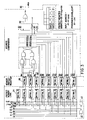
- Fig. 3 shows a schematic diagram of one embodiment of memory protection circuitry in accordance with the present invention.
- Fig. 4 shows a circuit diagram of the "lock-in" circuit using the PRDS instruction. Also included in Fig. 4 are the detail circuits for DET-A and DET-C blocks 24 and 26, respectively, which are shown in Fig. 3.
- the address comparator shown in Fig. 3 compares the input address A 0 -A 7 to the protect register address R 0 -R 7 and its output WEN is high when A n is less than R n .
- "PADX" in Fig. 4 is the internal test pad which is not bonded out and "EPR" stands for "Enable Protect Register".
- the basic memory protect register latch circuit 26 comprises two subcircuits, as shown in Fig. 4.
- the first subcircuit is a cross-coupled static latch which includes two P-channel field effect transistors 34 and 36 and two N-channel field effect transistors 38 and 40.
- the second subcircuit includes two nonvolatile memory transistors 42 and 44.
- the drains of transistors 34 and 38 are coupled to each other at node A.
- the drains of transistors 36 and 40 are coupled to each other at node B.
- the sources of transistors 34 and 36 are connected to the positive supply potential VCC.
- the sources of transistors 38 and 40 are connected to the ground potential VSS.
- the gates of transistors 34 and 38 are coupled together and are also coupled to node B.
- Transistors 42 and 44 are N-channel floating gate MOSFET devices in which the floating gates are formed in a polysilicon layer and the control gates are selectively defined in the bulk silicon by a buried N+ implant mask.
- the floating gate (node C) of the memory transistor 42 is capacitively coupled to its control gate (node D) via coupling capacitor 46.
- Coupling capacitor 46 is essentially formed by the overlap of the floating polysilicon gate and the buried N+ implant area exposed by the thin oxide mask, as illustrated in Fig. 5A.
- the floating gate (node E) of the memory transistor 44 is capacitively coupled to its control gate (node F) via the coupling capacitor 48.
- the floating gates of the transistors 42 and 44 are capacitively cross-coupled to the control gates of transistors 44 and 42, respectively, via relatively small area tunneling capacitors 50 and 52.
- the tunneling capacitors 52 and 50 are formed by the overlap of the floating gates of transistors 42 and 44 with the buried N+ implant areas which are exposed by the thin oxide mask and are electrically in common with the control gates of transistors 44 and 42, respectively.
- Both the coupling capacitors 46, 48 and the tunneling capacitors 50, 52 have relatively thin oxide (100 Angstroms) dielectrics between the floating gates and the control gates.
- the drain of the memory element 42 is coupled to node B, which was defined above in conjunction with the cross-coupled static latch.
- the drain of the memory element 44 is coupled to node A, which was also previously defined.
- the sources of both memory elements 42 and 44 are connected to the ground potential VSS.
- stray capacitances inherent in the layout of the latch shown in Fig. 2. These include the floating gate to control gate overlap capacitances in the nonthin-oxide areas and the capacitance due to the source and drain overlap to the floating gate in the memory transistors.
- Figs. 5A and 5B show the cross-sectional views of the memory cell elements 42 and 44.
- region 300 comprises the P-type silicon in which the highly doped N+ source and drain regions are formed for the N-channel CMOS transistors. Also formed in the region 300 are buried-N+ diffusions which are not as highly doped compared to the source/drain N+ regions. The buried-N+ regions are used to form the control gates of the memory transistors and can also be used for conductive underpasses in other parts of the circuitry.
- the control gates of transistors 42 and 44 are shown in the cross-sectional diagrams of Figs. 5A and 5B.
- the floating gates of transistors 42 and 44 are also shown in Figs. 5A and 5B and are comprised of conductive polycrystalline silicon.
- the floating polycrystalline gate of transistor 42 is separated from the crystalline silicon by the coupling oxide 46, the tunneling oxide 50, the gate oxide 54, the oxide over the buried-N+ region 301, and the field oxide 302.
- the oxide over the buried N+, region 301 is substantially thicker than the gate oxides 30 and 32.
- the field oxide, region, 302 is substantially thicker than the oxide in region 301.
- the floating gate of transistor 42 is also capacitively coupled to its own control gate due to the overlap of the floating polysilicon gate to its control gate formed by the oxide over the buried-N+ region in the silicon substrate, "Cbn+g.”
- Another component of the capacitance, "Cfld,” is due to the overlap of the floating polysilicon gate to the substrate in the field oxide regions 302.
- a high programming voltage "VPPI" (12-17v) must be applied to one of the two programming nodes D or F for about 5-10 ms.
- VPPI high programming voltage
- the other programming node F must be held at the ground potential.
- Rg Ccoup + Cbn+t Ccoup + Cbn+g + Ctun + Cfld + Cgox + Cbn+t
- the initial electric field "E” is of the order of 9-10 Mv/cm, then a sufficient number of electrons tunnel through the tunnel oxide onto the floating gate of transistor 42 storing a net negative charge on node C so as to make an appreciable positive shift in the threshold voltage of this device.
- E VPPI - Rg • VPPI Ttun
- the initial electric field "E" is of the order of 9-10 Mv/cm, then a sufficient number of electrons tunnel through the tunnel oxide out of the floating gate of transistor 44 storing a net positive charge on node E so as to make an appreciable negative shift in the threshold voltage of this device.
- the field "E” however decreases with time as more and more electrons tunnel through the tunnel oxide and are collected on the floating polycrystalline gate.
- the electric field "E” is so low that very few electrons tunnel through the oxide and further threshold voltage shift is negligible.
- the electric field "E′” also decreases with time as more electrons tunnel through the tunnel oxide out of the floating gate and eventually leave the floating gate with a net positive charge.
- the electric field "E′” at this point is so low that very few electrons tunnel through the tunnel oxide and further threshold voltage shift is negligible.
- the control gates of both the memory elements 42 and 44 are held at the ground potential and the electric fields across the tunnel oxides are minimal and are only due to the charges on the floating gates due to the programming operation.
- the two memory elements 42, 44 in the electrically alterable latch 26 remain programmed to their respective ERASED (enhancement) and WRITTEN (depletion) states.
- ERASED enhanced
- WRITTEN depletion
- node B pulls up to VCC and node A is pulled down to VSS.
- the two cross-coupled inverters are latched to their proper states and no dc power is consumed by the circuit.
- the current sinking capability of the written memory element should be such that it can pull the corresponding cross-coupled latch node low enough to set the latch to its proper programmed state.
- the latch circuit 26 described above can be used in conjunction with a high voltage inverter circuit 24, as shown in Fig. 1.
- the purpose of the protect register logic circuit 24 is to translate the low (VSS) and high (VCC) CMOS levels at its input into high (•VPPI 12-17v) and low (VSS) levels respectively.
- circuit 24 works like a high voltage inverter.
- a similar circuit block 24 can be connected to the control gate of memory element 44 shown in Fig. 4. This implementation is shown in Fig. 6. This circuit can be used to reset the DATAOUT (Node B) of the nonvolatile latch to a low (VSS) state, by taking the RESETB signal low during the program cycle.
- Fig. 6 shows one possible setup in which the nonvolatile latch circuit 26 could be used in accordance with the present invention.
- Circuit block 64 includes an "N" bit long register which has the nonvolatile latch circuit 26 described above as the basic building block.
- the circuit block 66 includes "N" high voltage inverter circuits 24 described above, the outputs of each feeding into the input of a corresponding nonvolatile latch 26 in the block 64.
- the top circuit block 24′ has "PROGB” and “PROG-DISABLEB” as the other inputs and its output “DISABLE” feeds into the control gate of one of the memory elements of the additional circuit block 26′.
- the control gate of the other memory element in the circuit block 26′ is connected to VSS.
- the output "PROG-DISABLE" of the circuit block 26′ serves as a common input to the remaining N+1 high voltage inverters 24.
- the second high voltage inverter 24 ⁇ outside of the circuit block 66 has its last remaining input connected to a signal called "RESETB” and its output “RESET” is connected to one input of each nonvolatile element in the circuit block 64.
- the last input of each high voltage inverter element in the circuit block 66 is connected to the input of the corresponding nonvolatile latch 26 in the circuit block 64 as shown in Fig. 6.
- the circuit block 64 can be disabled from further pattern changes by performing a PROG-DISABLE operation. This is done by taking the PROG-DlSABLE input to VSS during the programming operation with RESETB and ADDB1 - ADDBN all at VCC. This operation makes the signal PROG-DISABLE permanently high, thereby disabling all future pattern changes in the circuit block 64.
- a particular embodiment of the present invention is described below: a) device 10 in an 8-pin dual-in-line and small-outline package.
- a PE (Program Enable) pin provides extra security against accidental programming. The PE pin must be held “high” while loading any programming instruction. However, after loading the instruction, the PE pin becomes a "don't care”.
- a PRE (Protect Register Enable) pin is provided for all Protect-Register operations. Table 1 below lists the instructions for the device 10.
- VCC When VCC is first applied to the EEPROM device 10, it powers-up in the Write Disabled state, i.e. all programming modes must be preceded by a WRITE ENABLE (WEN) instruction. Once a WRITE ENABLE instruction is executed, programming remains enabled until a WRITE DISABLE (WDS) instruction is executed or VCC is removed from the device 10.
- WEN WRITE ENABLE
- WDS WRITE DISABLE
- This software solution to data security in addition to the hardware (PE pin) solution, provides virtually foolproof protection against an inadvertent Write Cycle. In order to Write or alter the address stored in the protect register 14, a precise sequence of instructions must be followed. Otherwise the instruction will be ignored. The proper sequence is as follows: first the device 10 must be Write Enabled, second the Protect Register Enable (PREN) instruction is executed.
- the PREN instruction must be followed immediately by a Protect Register Clear (PRCLEAR), Protect Register Write (PRWRITE), or a Protect Register Disable (PRDS) instruction.
- PRCLEAR Protect Register Clear
- PRWRITE Protect Register Write
- PRDS Protect Register Disable
- the protect register operations must follow this sequence exactly and are specifically intended to provide data security to the protect register 14.
- the PRCLEAR instruction clears the address stored in the protect register 14 and removes the Write protection from all registers in the array 12.
- the PRWRITE instruction is used to write into the protect register 14 the address of the first register in the array 12 to be protected. Thus, a user-defined field of addresses can be protected from Write operations.
- the PRDS instruction is a one-time-only instruction that renders the protect register 14 unalterable, allowing the specified registers to become permanently protected against data changes.
Landscapes
- Engineering & Computer Science (AREA)
- Theoretical Computer Science (AREA)
- Computer Security & Cryptography (AREA)
- Physics & Mathematics (AREA)
- General Engineering & Computer Science (AREA)
- General Physics & Mathematics (AREA)
- Computer Hardware Design (AREA)
- Read Only Memory (AREA)
- Storage Device Security (AREA)
Claims (2)
- Ein elektrisch löschbarer programmierbarer Nur-Lese-Speicher- (kurz: EEPROM)-Baustein (10), der eine Speichermatrix (12) mit einer Mehrzahl von elektrisch löschbaren programmierbaren Nur-Lese-Speicher-Datenspeicherregistern für das Speichern von Daten umfaßt, wobei jedem Datenspeicherregister eine entsprechende Zugriffsadresse zugeordnet ist, welche Zugriffsadressen die Datenspeicherregister sequentiell von einem Anfangsdatenspeicherregister zu einem Enddatenspeicherregister definieren, welcher EEPROM-Baustein ferner Mittel (20) umfaßt, die auf eine Lesezugriffsadresse für das Lesen von Daten, die in dem Datenspeicherregister entsprechend der Lesezugriffsadresse gespeichert sind, reagieren, mit Mitteln, die auf eine Löschzugriffsadresse für das elektrische Löschen von in einem Datenspeicherregister gespeicherten Daten entsprechend der Löschzugriffsadresse reagieren, und mit Mitteln, die auf eine Schreibzugriffsadresse reagieren für das Ändern von Daten, die in einem der Schreibzugriffsadresse entsprechenden Datenspeicherregister gespeichert sind, welcher EEPROM-Baustein gekennzeichnet ist durch:(a) ein EEPROM-Speicherschutzregister (14, 26), das die Zugriffsadresse eines ausgewählten Datenspeicherregisters als eine Schutzadresse speichert, welche Schutzadresse eine Abfolge von Datenspeicherregistern definiert mit Adressen gleich oder größer der Adresse des ausgewählten Datenspeicherregisters;(b) Mittel (13), die auf die Zugriffsadresse und auf die Schutzadresse reagieren für das Unterbinden der Veränderung von Daten, die in der Abfolge von Datenspeicherregistern, definiert durch die Schutzadresse,gespeichert sind; und(c) eine Schutzspeicherlogikschaltung (24), verbunden mit dem Speicherschutzregister (26) und auf ein extern zugeführtes Schutzregistersperrsignal (PRDS) reagierend, für das permanente Festlegen der Schutzadresse in dem Speicherschutzregister, um dadurch permanent jedes der Datenspeicherregister in der Abfolge von Datenspeicherregistern, definiert durch die Schutzadresse, aus einem elektrisch löschbaren programmierbaren Nur-Lese-Speicher-Datenspeicherregister in ein Nur-Lese-Datenspeicherregister umzuwandeln.
- Der Baustein nach Anspruch 1, ferner umfassend:(d) ein Befehlsregister (16), das einen binären Befehl empfängt, welcher die Zugriffsadresse als eine ausgewählte Schreibzugriffsadresse spezifiziert;(e) ein Datenschieberegister (18), das Daten empfängt, die in ein Datenspeicherregister entsprechend der ausgewählten Schreibzugriffsadresse einzuschreiben sind;(f) Schreibmittel (20), die auf den Empfang von Daten durch das Datenschieberegister reagieren für den Transfer von Daten von dem Datenschieberegister in das Datenspeicherregister mit einer Zugriffsadresse entsprechend der Schreibzugriffsadresse, wenn der Schreibzugriff zu dem entsprechenden Datenspeicherregister entsperrt worden ist;(g) einen Adreßdekoder (15), der auf den Empfang eines Schreibentsperrsignals und den Empfang der ausgewählten Schreibzugriffsadresse reagiert für das Entsperren des Schreibzugriffs zu einem Datenspeicherregister mit einer Zugriffsadresse entsprechend der ausgewählten Schreibzugriffsadresse, und wobei die genannten Mittel für das Unterbinden einen Adreßkomparator (13) für das Vergleichen der ausgewählten Schreibzugriffsadresse und der Schutzadresse umfassen und für das Bereitstellen des Schreibentsperrsignals an den Adreßdekoder nur dann, wenn das Datenspeicherregister entsprechend der ausgewählten Schreibzugriffsadresse nicht innerhalb der Abfolge von Datenspeicherregistern ist, definiert durch die Schutzadresse.
Applications Claiming Priority (2)
| Application Number | Priority Date | Filing Date | Title |
|---|---|---|---|
| US14937388A | 1988-01-28 | 1988-01-28 | |
| US149373 | 1988-01-28 |
Publications (3)
| Publication Number | Publication Date |
|---|---|
| EP0326053A2 EP0326053A2 (de) | 1989-08-02 |
| EP0326053A3 EP0326053A3 (de) | 1991-01-02 |
| EP0326053B1 true EP0326053B1 (de) | 1996-06-26 |
Family
ID=22529990
Family Applications (1)
| Application Number | Title | Priority Date | Filing Date |
|---|---|---|---|
| EP89101077A Expired - Lifetime EP0326053B1 (de) | 1988-01-28 | 1989-01-23 | Datensicherungsverfahren für einen programmierbaren Speicher |
Country Status (5)
| Country | Link |
|---|---|
| EP (1) | EP0326053B1 (de) |
| JP (1) | JPH025157A (de) |
| KR (1) | KR0127748B1 (de) |
| CA (1) | CA1322414C (de) |
| DE (1) | DE68926718T2 (de) |
Families Citing this family (7)
| Publication number | Priority date | Publication date | Assignee | Title |
|---|---|---|---|---|
| US5550997A (en) * | 1992-11-18 | 1996-08-27 | Canon Kabushiki Kaisha | In an interactive network board, a method and apparatus for preventing inadvertent loading of a programmable read only memory |
| FR2732487B1 (fr) * | 1995-03-31 | 1997-05-30 | Sgs Thomson Microelectronics | Procede de protection de zones de memoires non volatiles |
| FR2757654B1 (fr) * | 1996-12-24 | 1999-02-05 | Sgs Thomson Microelectronics | Memoire avec zones protegees en lecture |
| DE19738712C2 (de) * | 1997-09-04 | 2001-09-20 | Siemens Ag | Nichtflüchtiger Speicher mit zu Subblöcken zusammengefaßten Speicherzellen |
| FR2770327B1 (fr) * | 1997-10-24 | 2000-01-14 | Sgs Thomson Microelectronics | Memoire non volatile programmable et effacable electriquement comprenant une zone protegeable en lecture et/ou en ecriture et systeme electronique l'incorporant |
| US6526128B1 (en) * | 1999-03-08 | 2003-02-25 | Agere Systems Inc. | Partial voice message deletion |
| DE102006005480B3 (de) * | 2006-02-03 | 2007-02-22 | Technische Universität Clausthal | Mikroprozessor und Compiler |
Family Cites Families (4)
| Publication number | Priority date | Publication date | Assignee | Title |
|---|---|---|---|---|
| DE2842548A1 (de) * | 1978-09-29 | 1980-04-10 | Siemens Ag | Programmierbare speicherschutzlogik fuer mikroprozessorsysteme |
| US4573119A (en) * | 1983-07-11 | 1986-02-25 | Westheimer Thomas O | Computer software protection system |
| DE3514430A1 (de) * | 1985-04-20 | 1986-10-23 | Sartorius GmbH, 3400 Göttingen | Verfahren zum abspeichern von daten in einem elektrisch loeschbaren speicher und elektrisch loeschbarer speicher zur durchfuehrung des verfahrens |
| US4835733A (en) * | 1985-09-30 | 1989-05-30 | Sgs-Thomson Microelectronics, Inc. | Programmable access memory |
-
1989
- 1989-01-23 EP EP89101077A patent/EP0326053B1/de not_active Expired - Lifetime
- 1989-01-23 DE DE68926718T patent/DE68926718T2/de not_active Expired - Fee Related
- 1989-01-27 KR KR1019890000885A patent/KR0127748B1/ko not_active Expired - Fee Related
- 1989-01-27 CA CA000589323A patent/CA1322414C/en not_active Expired - Fee Related
- 1989-01-30 JP JP1017850A patent/JPH025157A/ja active Pending
Also Published As
| Publication number | Publication date |
|---|---|
| KR0127748B1 (ko) | 1998-10-01 |
| DE68926718T2 (de) | 1997-02-20 |
| KR890012316A (ko) | 1989-08-25 |
| CA1322414C (en) | 1993-09-21 |
| DE68926718D1 (de) | 1996-08-01 |
| EP0326053A3 (de) | 1991-01-02 |
| EP0326053A2 (de) | 1989-08-02 |
| JPH025157A (ja) | 1990-01-10 |
Similar Documents
| Publication | Publication Date | Title |
|---|---|---|
| US4975878A (en) | Programmable memory data protection scheme | |
| EP0326883B1 (de) | Elektrisch veränderliches nichtflüchtiges Flip-Flop mit Null-Leistung | |
| US5197034A (en) | Floating gate non-volatile memory with deep power down and write lock-out | |
| US4744062A (en) | Semiconductor integrated circuit with nonvolatile memory | |
| KR950014560B1 (ko) | 불휘발성 기억 장치 | |
| EP1143455B1 (de) | Nichtflüchtige Halbleiterspeicheranordnung | |
| US5673222A (en) | Nonvolatile semiconductor memory device | |
| KR0172366B1 (ko) | 불휘발성 반도체 메모리 장치의 독출 및 프로그램 방법과 그 회로 | |
| US6031757A (en) | Write protected, non-volatile memory device with user programmable sector lock capability | |
| US4975883A (en) | Method and apparatus for preventing the erasure and programming of a nonvolatile memory | |
| US5349249A (en) | Programmable logic device having security elements located amongst configuration bit location to prevent unauthorized reading | |
| EP0645774B1 (de) | Speicherschutzschaltung für EPROM | |
| EP0326053B1 (de) | Datensicherungsverfahren für einen programmierbaren Speicher | |
| US4680736A (en) | Method for operating a user memory designed a non-volatile write-read memory, and arrangement for implementing the method | |
| US4849942A (en) | Protection device for an erasable and reprogrammable read only memory | |
| WO1996008825A1 (en) | Memory with multiple erase modes | |
| US4545038A (en) | Precharged discharge sensing for EPROM | |
| Hieda et al. | Optimum design of dual-control gate cell for high-density EEPROM's | |
| KR930001653B1 (ko) | 불휘발성 반도체 기억장치 | |
| JP4642017B2 (ja) | 不揮発性半導体記憶装置用セクタ保護回路、セクタ保護方法、および不揮発性半導体記憶装置 | |
| JP2833621B2 (ja) | 不揮発性記憶装置 | |
| US6044006A (en) | Method for programming a ROM cell arrangement | |
| KR20070042501A (ko) | 불휘발성 반도체 기억장치용 섹터 보호 회로, 섹터 보호방법 및 불휘발성 반도체 기억장치 | |
| KR0172336B1 (ko) | 불 휘발성 반도체 메모리의 프로그램 검증 및 금지 방법과 그 회로 |
Legal Events
| Date | Code | Title | Description |
|---|---|---|---|
| PUAI | Public reference made under article 153(3) epc to a published international application that has entered the european phase |
Free format text: ORIGINAL CODE: 0009012 |
|
| AK | Designated contracting states |
Kind code of ref document: A2 Designated state(s): DE FR GB IT NL |
|
| PUAL | Search report despatched |
Free format text: ORIGINAL CODE: 0009013 |
|
| AK | Designated contracting states |
Kind code of ref document: A3 Designated state(s): DE FR GB IT NL |
|
| 17P | Request for examination filed |
Effective date: 19910508 |
|
| 17Q | First examination report despatched |
Effective date: 19930518 |
|
| GRAH | Despatch of communication of intention to grant a patent |
Free format text: ORIGINAL CODE: EPIDOS IGRA |
|
| GRAH | Despatch of communication of intention to grant a patent |
Free format text: ORIGINAL CODE: EPIDOS IGRA |
|
| GRAA | (expected) grant |
Free format text: ORIGINAL CODE: 0009210 |
|
| AK | Designated contracting states |
Kind code of ref document: B1 Designated state(s): DE FR GB IT NL |
|
| PG25 | Lapsed in a contracting state [announced via postgrant information from national office to epo] |
Ref country code: IT Free format text: LAPSE BECAUSE OF FAILURE TO SUBMIT A TRANSLATION OF THE DESCRIPTION OR TO PAY THE FEE WITHIN THE PRE;WARNING: LAPSES OF ITALIAN PATENTS WITH EFFECTIVE DATE BEFORE 2007 MAY HAVE OCCURRED AT ANY TIME BEFORE 2007. THE CORRECT EFFECTIVE DATE MAY BE DIFFERENT FROM THE ONE RECORDED.SCRIBED TIME-LIMIT Effective date: 19960626 Ref country code: NL Free format text: LAPSE BECAUSE OF FAILURE TO SUBMIT A TRANSLATION OF THE DESCRIPTION OR TO PAY THE FEE WITHIN THE PRESCRIBED TIME-LIMIT Effective date: 19960626 Ref country code: FR Effective date: 19960626 |
|
| REF | Corresponds to: |
Ref document number: 68926718 Country of ref document: DE Date of ref document: 19960801 |
|
| EN | Fr: translation not filed | ||
| NLV1 | Nl: lapsed or annulled due to failure to fulfill the requirements of art. 29p and 29m of the patents act | ||
| PG25 | Lapsed in a contracting state [announced via postgrant information from national office to epo] |
Ref country code: GB Effective date: 19970123 |
|
| PLBE | No opposition filed within time limit |
Free format text: ORIGINAL CODE: 0009261 |
|
| STAA | Information on the status of an ep patent application or granted ep patent |
Free format text: STATUS: NO OPPOSITION FILED WITHIN TIME LIMIT |
|
| 26N | No opposition filed | ||
| GBPC | Gb: european patent ceased through non-payment of renewal fee |
Effective date: 19970123 |
|
| PGFP | Annual fee paid to national office [announced via postgrant information from national office to epo] |
Ref country code: DE Payment date: 20040301 Year of fee payment: 16 |
|
| PG25 | Lapsed in a contracting state [announced via postgrant information from national office to epo] |
Ref country code: DE Free format text: LAPSE BECAUSE OF NON-PAYMENT OF DUE FEES Effective date: 20050802 |