EP0321133B1 - Circuit intégré à semi-conducteur avec une fonction de test à courant continu - Google Patents
Circuit intégré à semi-conducteur avec une fonction de test à courant continu Download PDFInfo
- Publication number
- EP0321133B1 EP0321133B1 EP88311498A EP88311498A EP0321133B1 EP 0321133 B1 EP0321133 B1 EP 0321133B1 EP 88311498 A EP88311498 A EP 88311498A EP 88311498 A EP88311498 A EP 88311498A EP 0321133 B1 EP0321133 B1 EP 0321133B1
- Authority
- EP
- European Patent Office
- Prior art keywords
- signal
- circuit
- output
- reset
- test
- Prior art date
- Legal status (The legal status is an assumption and is not a legal conclusion. Google has not performed a legal analysis and makes no representation as to the accuracy of the status listed.)
- Expired - Lifetime
Links
Images

Classifications
-
- G—PHYSICS
- G11—INFORMATION STORAGE
- G11C—STATIC STORES
- G11C29/00—Checking stores for correct operation ; Subsequent repair; Testing stores during standby or offline operation
-
- G—PHYSICS
- G01—MEASURING; TESTING
- G01R—MEASURING ELECTRIC VARIABLES; MEASURING MAGNETIC VARIABLES
- G01R31/00—Arrangements for testing electric properties; Arrangements for locating electric faults; Arrangements for electrical testing characterised by what is being tested not provided for elsewhere
- G01R31/28—Testing of electronic circuits, e.g. by signal tracer
- G01R31/30—Marginal testing, e.g. by varying supply voltage
-
- G—PHYSICS
- G01—MEASURING; TESTING
- G01R—MEASURING ELECTRIC VARIABLES; MEASURING MAGNETIC VARIABLES
- G01R31/00—Arrangements for testing electric properties; Arrangements for locating electric faults; Arrangements for electrical testing characterised by what is being tested not provided for elsewhere
- G01R31/28—Testing of electronic circuits, e.g. by signal tracer
- G01R31/317—Testing of digital circuits
- G01R31/31701—Arrangements for setting the Unit Under Test [UUT] in a test mode
Definitions
- the present invention relates to a semiconductor integrated circuit having a DC test function, and more particularly to a semiconductor integrated circuit able to test the DC characteristics without a deterioration of the AC characteristics.
- a method of testing a large scale integrated circuit (LSI) device consists of inputting a test pattern or signal to an LSI device under test, comparing an output value from the LSI device to determine whether or not a function of the LSI device is faulty, and measuring analogue-values of an input/output voltage or current and the like.
- LSI large scale integrated circuit
- a DC characteristic test and an AC characteristic test are used in the same way for a small scale integrated circuit (SSI) or a medium scale integrated circuit (MSI), based on the test method used for an LSI.
- SSI small scale integrated circuit
- MSI medium scale integrated circuit
- the DC characteristic test measures the voltage of external terminals, which are an input terminal and a power source terminal, of an LSI device or the DC current passing through the external terminals in a known DC testing method, and the AC characteristic test measures a propagation delay time between input/output terminals, a transition duration of the output waveform, a set-up time of the input waveform, a holding time, the minimum clock pulse width, and the maximum clock frequency or the like.
- LSI large scale integrated circuit
- a first test circuit and a second test circuit are arranged between an internal main circuit and an output buffer circuit, and the DC test of an LSI device is effected by using these test circuits.
- a deterioration of the AC characteristics occurs due to the delay caused by the DC test circuit.
- One of the AC characteristics is a propagation delay time between an input terminal and an output terminal, and when a signal is applied to an input pin or terminal in synchronization with a predetermined clock signal, the delay of a signal output from an output pin can be measured by the AC test as a propagation delay time within an LSI device.
- a signal is delayed by passing through gates of the first and second test circuits; i.e., the signal is delayed due to factors other than the essential function of the interior logic of the LSI device, and the AC characteristics deteriorate.
- the LSI appears to be faulty in having an unacceptably large delay but this occurs only when the device is under test with the first and second circuits in operation.
- an integrated circuit for receiving an input signal and producing an output signal comprising: an internal main circuit for carrying out various logic operations in accordance with the input signal and producing a first signal and second signal; a set/reset circuit, operatively connected to the internal main circuit, being set in response to the first signal and reset in response to the second signal in a normal mode; an output buffer circuit, connected to the set/reset circuit, for producing the output signal in response to an output of the set/reset circuit; and testing means for generating predetermined output signals during testing; characterised in that the testing means comprises a control circuit connected between the internal main circuit and the set/reset circuit, for receiving the first signal, a reset signal for initializing the internal main circuit, and a first test signal, further characterised in that, during a first DC test mode, the control circuit sets the set/reset circuit in response to the receipt of the first test signal regardless of the first signal and the reset signal for initializing the internal main circuit and during the second DC test mode, the control circuit resets the set/reset circuit in response to
- An advantage of the present invention is the provision of a semiconductor integrated circuit device able to test the DC characteristics without the deterioration of the AC characteristics, by incorporating the DC test conditions into a hardware reset condition, a reset condition or the like produced from an internal logic block.
- a hardware-reset is effected prior to a DC test and the set/reset circuit is held at a reset state, the output buffer circuit at an initialisation state, and further, a gate-ON signal is not output.
- a test signal is incorporated into one of a set condition and a reset condition, and therefore, a DC test circuit does not interfere with the AC characteristics of an LSI device and these characteristics are not deteriorated.
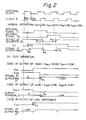
- the integrated circuit of Figure 1 is constituted by an internal main circuit 52, a set/reset circuit 1, testing circuits 11 and 13, an output buffer 12, input pins 51, a reset pin 54, test pins 55, 551, 56, 57 and output pins 21.
- reference numeral 1 denotes a set/reset circuit constituted by NOR gates 1 and 4 which form a set/reset flip-flop 2, abbreviated as S-R FF, AND gates 5 and 6, and an OR gate 7.
- An input signal is input to an internal main circuit 52 through input pins 51 and processed.
- Internal signals S1 and S2 as shown in Figure 2 that is, the outputs of the internal main circuit 52 are output to output pins 21 through a set/reset circuit 1, a first testing circuit 11 and an output buffer 12. If the internal main circuit 52 is constituted by a set of complicated logic circuits, it takes too long to set a state of output pin 21 by an input signal given to at least one of input pins 51.
- an output of an inverter 8 and a signal G C pass through a first testing circuits 11 and a second testing circuit 13 just as it is, respectively.
- the state of the output pins 21 can be set to a HIGH state, a LOW state or a high impedance (Z) state.
- all of output pins 21 can be set to a HIGH state, a LOW state or a high impedance state.
- the S-R FF 2 is set by the internal signals S1 and reset by the internal signal S2.
- the internal main circuit 52 is initialized by the hardware reset signal H-RESET.
- the internal signal S2 or the hardware reset signal (H-RESET) at a RESET PIN 54 is input to the AND gate 5 through the OR gate 7, and each of the above-noted signals is output to the S-R FF 2 in synchronization with a clock ⁇ .
- the internal signal S1 is input to the AND gate 6 and the internal signal S1 also output to the S-R FF 2 in synchronization with the clock ⁇ .
- An output of the set/reset circuit 1 is inverted by an inverter 8, the inverted signal is sent to an output buffer circuit 12 through a first test circuit 11, and further, an output of a second that circuit 13 is input to the output buffer circuit 12.
- the first test circuit 11 is constituted by P-channel MOS transistors 14 to 16, referred to as PMOS hereinafter, and N-channel MOS transistors (NMOS) 17 to 19.
- a test signal V OH which denotes that HIGH is active, is input to gates of the PMOS 14, and NMOS 19 and a test signal V OLX , which denotes that LOW is active, is input to gates of the NMOS 18 and PMOS 16.
- V OH or V OLX is active, regardless of the level of the signal output from the set/reset circuit 1, an output terminal 21 of the LSI device is forcibly brought to a HIGH level state or a LOW level state to effect a DC test.
- the first test circuit 11 is a circuit which brings to set forcibly a state of the output pin 21 to a HIGH or LOW level state.
- a first testing circuit 11 When a test signal V OH or V OLX is input, a first testing circuit 11, regardless of a signal output from the set/reset circuit 1, outputs an HIGH level or an LOW level signal to the output buffer circuit 12 through an inverter 20.
- the output buffer circuit 12 is formed by a NAND gate 31, a NOR gate 32, an inverter 33, a PMOS 34, and an NMOS 35, and buffer-amplifies an input signal to output same to an output terminal.
- the second testing circuit 13 is a circuit which sets forcibly a state of the output pin 21 to a high impedance state (Z).
- a second test circuit 13 is formed by PMOS's 41 to 43, NMOS's 44 to 47, and an inverter 48, and a gate-ON signal G on is input to a gate of a PMOS 41, a gate control signal G C is input to each gate of a PMOS 42 and an NMOS 44, where both gates are connected to each other, and a gate-OFF signal G OFF is input to a gate of an NMOS 45 through an inverter 48.
- the second test circuit 13 controls the output buffer circuit 12, i.e., determines whether or not the output buffer circuit 12 is enabled.
- signals G ON and G OFF are employed for a DC test and a signal G C is used during a normal operation.
- a normal operation i.e., when a DC test is not effected, the signals G ON and G OFF are in an LOW level state and only a signal G C is valid.
- the signal G C is a gate control signal during a normal operation, and when the signal G C is active, i.e. in a HIGH level active, i.e. in a HIGH level state, an output level of an inverter 20 appears at an output terminal 21 as it is.
- the signal G C is inactive, i.e. in a LOW level state, the output pin 21 is in a high impedance state (Z) of a three-state condition.
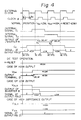
- Figure 2 shows the waveforms of the signals in a main parts of in Fig. 1. Based on the receipt of an external clock, a clock ⁇ is produced with a time delay, and accordingly, a normal operation and a DC operation of the LSI device are carried out. An internal signal S1 is followed by an internal signal S2 and an output of an inverter 20 is delayed by a time delay ⁇ 4.
- G ON is the same as above and the waveform of G OFF is slightly delayed at the leading edge, compared with that of the V OLX .
- the output of an inverter 49 is in an LOW level state, and therefore, the output of the LSI device is in a high impedance (Z) state as shown in the third waveforms.
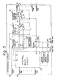
- FIG. 3 A semiconductor integrated circuit having a DC test function according to an embodiment of the present invention is shown in Fig. 3.
- the waveforms of the signals in the essential blocks in Fig. 3 are shown in Fig. 4.
- an LSI device is constituted by an internal main circuit 52 (for example, a microprocessor, a PMA controller, a peripheral controller, etc.) output buffer 12, input pins 81, output pins 21, and test pins 82 and 83.
- an internal main circuit 52 for example, a microprocessor, a PMA controller, a peripheral controller, etc.
- output buffer 12 input pins 81, output pins 21, and test pins 82 and 83.
- the output buffer 12 has a PMOS 34, a NMOS 35, a NAND gate 31, a NOR gate 32, and an inverter 33, the internal main circuit 52 carries out a variety of logical operations to deliver of setting and resetting condition signals to the output buffer, and on the other hand, is supplied with a hardware reset signal (H-RESET) signal from the reset pin 84 during a hardware resetting period.
- H-RESET hardware reset signal
- setting or resetting is an operation in which the data is stored temporarily in register or the like in internal logic circuits and after a lapse of a predetermined time a HIGH-active signal synchronized with the clock signal ⁇ is delivered.
- the hardware resetting is a resetting for forcibly resetting the logic circuit in the LSI device, for example, a resetting by an initialization. Normally, for a DC test, the hardware is reset to initialize all elements, and the DC test is started in this condition.
- the command signal for hardware resetting is H-RESET, which is supplied to the internal main circuit 52 and output buffer 52 from outside via the reset pin 84. Further, the internal main circuit 52 supplies a gate control signal G c to control the output buffer circuit 12.
- the gate control signal G c is effective when V OLX which is first DC test signal, and V OH which is second DC test signal are inactive in the condition shown in Fig. 3.
- the test pins 82 and 83 are provided to receive the first test signal V OLX and second test signal V OH when a DC test is carried out.
- Signals V OLX and V OH may be supplied from the mode register-1 and mode register-2 without providing test pins 82 and 83.
- the mode register-1 delivers signals V OLX and mode register-2 delivers signal V OH in accordance with commands from the internal main circuit 52.
- the internal signal S2 is supplied from the internal main circuit 52 to the OR gate 7 to which an output from the AND gate 58 is supplied from the OR gate 7.
- the V OLX signal is inverted by the inverter 62 and supplied to the OR gate 59, and is supplied to the OR gate 60 through the inverter 61.
- the OR gate 59 is supplied with the internal signal S1.
- This OR gate 59 will set the set/reset circuit 1 when internal signal S1 or an LOW-active V OLX signal.
- the set/reset circuit 1 provides an HIGH-level signal when the setting internal signal S1, is supplied or V OLX signal is at LOW level, and delivers an LOW-level signal when supplied with the internal signal S2 or H-RESET signal. Therefore, the V OLX signal for a DC test is one of the signals input to the set/reset circuit 1. It should be noted that the set/reset circuit operation is based on the clock ⁇ .
- the above-mentioned AND gate 58, OR gate 59, and inverter 62 together form control circuit 71.
- the output signal from the set/reset circuit 1 is supplied via the inverter 8 to the output buffer circuit 12, which buffer-amplifies the signal level of the set/reset circuit 1 and delivers an inverted level signal to the output pin 21.
- the output buffer 12 is supplied with a signal from the OR gate 60 which is supplied with a test signal V OH , gate control signal GATE ON condition and the output of the inverter 61.
- the gate control signal is such that unless a test is made, the gate of the output buffer 12 is opened to permit a normal signal from the set/reset circuit 1 to be passed. When a test is made, the gate control signal is not effective, so that the above-mentioned normal signal cannot be passed as it is.
- test signals V OH When in the normal mode, test signals V OH is fixed in a LOW level state and V OLX is fixed in a HIGH level state.
- the LSI device 50 follows the normal logical request with the generation of a signal having a predetermined level. More particularly, the internal main circuit 52 generates the internal signals S1 and S2, and this command signal S1 and S2 are delivered to the set/reset circuit 1.
- the internal main circuit 52 supplies gate control signal G C to the OR gate 60. When the gate control signal G C becomes HIGH-active, the output buffer 12 permits the output signal from the inverter 8 to be passed.
- one of the input terminals of the NOR gate 32 is supplied with the HIGH-level signal from the inverter 8, and at the other terminal thereof, is supplied with an HIGH-level signal from the inverter 33, which has been inverted to LOW-Level by the inverter 33, so that the output is at LOW-Level and NMOS 35 is turned OFF.
- the output pin 21 is charged by a High-level power source V cc so that the output pin 21 is at HIGH level, i.e. HIGH-level signal is delivered.
- the output pin 21 is at HIGH- level for a resetting condition.
- the condition output is supplied through the OR gate 59 to the set/reset circuit 1 which, in turn, generates an HIGH-level signal in synchronization with the clock ⁇ and delivers an LOW-level signal through the inverter 8 to the output buffer 12.
- the output of the NAND gate 31 becomes HIGH and the output of the NOR gate 32 also becomes HIGH, so that the PMOS 34 is turned OFF and the NMOS 35 is turned ON.
- the potential at the output pin 21 drops to the ground potential, and thus the output pin 21 is at LOW-level, an LOW-level signal is delivered.
- the internal main circuit 52 commands a high impedance (Z), for example, as one of three states, from time to time.
- Z high impedance
- the condition in this case is such that a command is issued to prevent the GATE ON conditions from being effective when in the normal mode (namely, the signals V OLX and V OH are all inactive). Therefore, the GATE ON condition becomes inactive, i.e. LOW Level, so that all of the three signals input to the OR gate 60 are brought to the LOW-level and supplied to the output buffer 12.
- the output from the NAND gate 31 is at HIGH level and the output from the NOR gate 32 is at LOW Level , regardless of the level of the signal from the inverter 8, so that both the PMOS 34 and NMOS 35 are turned OFF, with the result that the output pin 21 is at a high impedance (Z) level, at which the impedance is high.
- the AC test is made in such a normal condition to measure the propagation delay time between, for example, the aforementioned input and output pins or terminals, and the set-up time, and the like.
- an external HIGH-active H-RESET signal is applied to the reset pin 74.
- the V OLX signal is HIGH-inactive while V OH signal is LOW-inactive, and the signal G C is LOW-inactive. Namely, all the signals are initialized to be inactive.
- the internal logic of the internal main circuit 52 is reset to the initial state.
- the H-RESET signal is supplied via the AND gate 58 to the set/reset circuit 1, which will be reset, so that an HIGH-level signal is supplied to the output buffer 12.
- the output pin 21 has a high impedance as in the case of a high impedance (Z) as one of three states, i.e., an initialization is attained.
- the DC test is made during the above-mentioned hardware resetting period. Namely, in the first DC test, an LOW-active V OLX signal is applied to the test pin 82. After inversion by the inverter 62 to the H level, this V OLX signal is delivered to the set/reset circuit 1 through the OR gage 59, and therefore, the set/reset circuit 1 is brought to a state as if it were supplied with an HIGH-level signal for a setting condition, and the output of this set/reset circuit 1 is at HIGH level and is supplied to the output buffer 12 through the inverter 8. On the other hand, an Low-level V OLX signal is applied to the AND gate 58 at this time so that the H-RESET signal cannot pass through the AND gate 58.
- the setting and resetting conditions are simultaneously supplied to the set/reset circuit 1, and the set/reset circuit 1 will not oscillate.
- the V OLX signal is supplied to the output buffer 12 through the OR gate 60. Therefore, the gate of the output buffer 12 is opened so that the aforementioned LOW-level signal from the set/reset circuit 1 is accepted by the output buffer 12, the output of which, namely, the output pin 21 is at the LOW-level , and thus the first DC test is effected.
- an HIGH-active V OH signal is supplied to the test pin 83.
- This V OH signal is supplied to the output buffer 12 through the OR gate 60 so that the signal levels at the other inputs of the NAND gate 31 and NOR gate 32, respectively, in the output buffer 12 are changed. Namely, the signal level at one of the inputs of the NAND gate 31 is HIGH and that at the other input is changed from LOW to HIGH, but the output of the NAND gate 31 is at LOW-Level .
- the signal level at one of the inputs of the NOR gate 32 is LOW and that at the other input is changed from LOW to HIGH, so that the output of the NOR gate 32 is changed from HIGH to LOW and the NMOS 35 is turned OFF.
- the output pin 21 is at the HIGH level, and the second DC test is made.
- the state wherein the set/reset circuit 1 is forcibly kept in the reset state by the hardware resetting signal H-RESET is cancelled, and due to this V OLX signal, a signal equivalent to the setting condition is supplied to the set/reset circuit 1.
- the output of the set/reset circuit 1 becomes HIGH, i.e. set state, and the gate of the output buffer 12 is opened so that the output of the output buffer 12 is at the LOW-level . Consequently, the V OLX signal is simply one of the conditions for setting the set/reset circuit 1, and since a test circuit is not included as in the prior art, between the set/reset circuit 1 and output buffer 12, the AC characteristics are not degraded.
- the gate of the output buffer 12 is opened in a state wherein the set/reset circuit 1 is in the reset condition due to the H-RESET signal, a signal equivalent to the internal signal S2 is supplied to the output buffer 12, the output of which is at HIGH level. Therefore, the V OH signal is simply one of the gate control signals for the output buffer 12 and the AC characteristics will not be degraded as in the abovementioned case. As a result, the AC characteristics of the LSI device can be improved and the quality of the operation of the device can be enhanced.
- the signals V OLX and V OH are made inactive during a hardware resetting, a signal of a high impedance (Z) is obtained at the output pin 21.
- Figure 4 shows waveforms for illustrating a normal operation and a DC operation of Fig. 3.
- V OH LOW
- V OLX HIGH
- H-RESET LOW
- the output of an inverter 8 produces a predetermined time delay ⁇ 0 to a clock ⁇ .
- the output of the LSI output terminal 21 is shown as high impedance (Z), HIGH level (H), LOW level (L), HIGH level (H), high impedance (Z), and so on as shown in the figure in case of an AC standard.
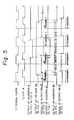
- Figure 5 shows waveforms for illustrating the outputs of the inverters 8, 20, 49 and the terminal 21 in Figs. 1 and 3.
Landscapes
- Engineering & Computer Science (AREA)
- General Engineering & Computer Science (AREA)
- Physics & Mathematics (AREA)
- General Physics & Mathematics (AREA)
- Tests Of Electronic Circuits (AREA)
- Logic Circuits (AREA)
- Testing Or Measuring Of Semiconductors Or The Like (AREA)
- Semiconductor Integrated Circuits (AREA)
Claims (3)
- Circuit intégré recevant un signal d'entrée et produisant un signal de sortie comprend:
un circuit principal interne (52) pour effectuer différentes opérations logiques en fonction du signal d'entrée et pour produire un premier signal (S₁) et un second signal (S₂);
un circuit de mise en service/remise à zéro (1), relié fonctionnellement au circuit principal interne (52), étant mis en service, en réponse au premier signal (S₁) et remis à zéro en réponse au second signal (S₂) en mode normal;
un circuit tampon de sortie (12), relié au circuit de mise en service/remise à zéro (1), pour produire le signal de sortie en réponse à une sortie du circuit de mise en service/remise à zéro (1); et
un moyen de test pour générer des signaux de sortie prédéterminés pendant le test;
caractérisé en ce que le moyen de test comprend un circuit de commande (71) relié au circuit principal interne (52) et au circuit de mise en service/remise à zéro (1), pour recevoir le premier signal (S₁), un signal de remise à zéro pour initialiser le circuit principal interne (52) et un premier signal de test (VOLX),
caractérisé en outre en ce que, pendant un premier mode de test en courant continu, le circuit de commande (71) met en service le circuit de mise en service/remise à zéro (1) en réponse à la réception du premier signal de test (VOLX) indépendamment du premier signal (S₁) et du signal de remise à zéro pour initialiser le circuit principal interne (52) et pendant le second mode de test en courant continu, le circuit de commande (71) remet à zéro le circuit de mise en service/remise à zéro (1) en réponse à la réception du signal de remise à zéro indépendamment du second signal (S₂). - Circuit intégré selon la revendication 1, dans lequel le circuit tampon de sortie comprend un circuit tampon à trois états (12) et le circuit principal interne (52) produit un signal de commande de porte (GC) pour commander le circuit tampon à trois états (12).
- Circuit intégré selon la revendication 2, dans lequel le circuit intégré comprend en outre un générateur de signal de porte (72), relié au circuit principal interne (52) et au circuit tampon à trois états (12) et recevant le signal de commande de porte (GC) et un second signal de test (VOH) et en rendant actif le circuit tampon à trois états (12) en réponse à la réception du second signal de test (VOH) indépendamment du signal de commande de porte (GC) pendant les modes de test en courant continu.
Applications Claiming Priority (2)
| Application Number | Priority Date | Filing Date | Title |
|---|---|---|---|
| JP307930/87 | 1987-12-04 | ||
| JP62307930A JP2579327B2 (ja) | 1987-12-04 | 1987-12-04 | 半導体集積回路 |
Publications (2)
| Publication Number | Publication Date |
|---|---|
| EP0321133A1 EP0321133A1 (fr) | 1989-06-21 |
| EP0321133B1 true EP0321133B1 (fr) | 1993-08-25 |
Family
ID=17974881
Family Applications (1)
| Application Number | Title | Priority Date | Filing Date |
|---|---|---|---|
| EP88311498A Expired - Lifetime EP0321133B1 (fr) | 1987-12-04 | 1988-12-05 | Circuit intégré à semi-conducteur avec une fonction de test à courant continu |
Country Status (5)
| Country | Link |
|---|---|
| US (1) | US4904883A (fr) |
| EP (1) | EP0321133B1 (fr) |
| JP (1) | JP2579327B2 (fr) |
| KR (1) | KR910007411B1 (fr) |
| DE (1) | DE3883504T2 (fr) |
Families Citing this family (12)
| Publication number | Priority date | Publication date | Assignee | Title |
|---|---|---|---|---|
| DE69020364T2 (de) * | 1989-07-13 | 1996-02-29 | Curtis Instr | Methode und Vorrichtung zum Kodieren und Lesen von Daten. |
| US5095267A (en) * | 1990-03-19 | 1992-03-10 | National Semiconductor Corporation | Method of screening A.C. performance characteristics during D.C. parametric test operation |
| US5070296A (en) * | 1990-06-22 | 1991-12-03 | Honeywell Inc. | Integrated circuit interconnections testing |
| US5181203A (en) * | 1990-12-21 | 1993-01-19 | Vlsi Technology, Inc. | Testable power-on-reset circuit |
| US5260950A (en) * | 1991-09-17 | 1993-11-09 | Ncr Corporation | Boundary-scan input circuit for a reset pin |
| US5841965A (en) * | 1994-05-16 | 1998-11-24 | Ricoh Company, Ltd. | System and method for automatically determining test point for DC parametric test |
| CN1439101A (zh) * | 1998-06-16 | 2003-08-27 | 因芬尼昂技术股份公司 | 用于测量和分析集成电路块的电信号的装置 |
| US6370675B1 (en) * | 1998-08-18 | 2002-04-09 | Advantest Corp. | Semiconductor integrated circuit design and evaluation system using cycle base timing |
| JP3942765B2 (ja) * | 1999-03-15 | 2007-07-11 | 株式会社アドバンテスト | 半導体デバイスシミュレート装置及びそれを用いた半導体試験用プログラムデバッグ装置 |
| JP3719654B2 (ja) * | 2001-05-10 | 2005-11-24 | 松下電器産業株式会社 | Lsiテスト方法 |
| DE10255665B4 (de) * | 2002-11-28 | 2008-05-08 | Qimonda Ag | Schaltung und Verfahren zur Bestimmung wenigstens eines Spannungs-, Strom- und/oder Leistungswerts einer integrierten Schaltung |
| JP2009025054A (ja) * | 2007-07-18 | 2009-02-05 | Panasonic Corp | 半導体検査回路、および半導体検査方法 |
Family Cites Families (8)
| Publication number | Priority date | Publication date | Assignee | Title |
|---|---|---|---|---|
| US4410991A (en) * | 1981-06-03 | 1983-10-18 | Gte Laboratories Incorporated | Supervisory control apparatus |
| DE3373759D1 (en) * | 1982-06-09 | 1987-10-22 | Fujitsu Ltd | One-chip semiconductor device incorporating a power-supply-potential detecting circuit with reset function |
| US4546472A (en) * | 1983-01-27 | 1985-10-08 | Intel Corporation | Method and means for testing integrated circuits |
| US4583041A (en) * | 1983-05-31 | 1986-04-15 | Takeda Riken Co., Ltd. | Logic circuit test system |
| US4803682A (en) * | 1985-03-04 | 1989-02-07 | Sanyo Electric Co., Ltd. | Resetting system |
| JPS61265829A (ja) * | 1985-05-20 | 1986-11-25 | Fujitsu Ltd | 半導体集積回路 |
| JPS62239221A (ja) * | 1986-04-10 | 1987-10-20 | Toshiba Corp | ワ−ドプロセツサ |
| KR900002770B1 (ko) * | 1986-08-04 | 1990-04-30 | 미쓰비시 뎅끼 가부시끼가이샤 | 반도체 집적회로장치 |
-
1987
- 1987-12-04 JP JP62307930A patent/JP2579327B2/ja not_active Expired - Fee Related
-
1988
- 1988-12-01 US US07/278,503 patent/US4904883A/en not_active Expired - Lifetime
- 1988-12-04 KR KR1019880016150A patent/KR910007411B1/ko not_active IP Right Cessation
- 1988-12-05 EP EP88311498A patent/EP0321133B1/fr not_active Expired - Lifetime
- 1988-12-05 DE DE88311498T patent/DE3883504T2/de not_active Expired - Fee Related
Also Published As
| Publication number | Publication date |
|---|---|
| US4904883A (en) | 1990-02-27 |
| US4904883B1 (fr) | 1993-02-02 |
| DE3883504D1 (de) | 1993-09-30 |
| JP2579327B2 (ja) | 1997-02-05 |
| KR890010922A (ko) | 1989-08-11 |
| DE3883504T2 (de) | 1993-12-09 |
| JPH01149447A (ja) | 1989-06-12 |
| EP0321133A1 (fr) | 1989-06-21 |
| KR910007411B1 (ko) | 1991-09-25 |
Similar Documents
| Publication | Publication Date | Title |
|---|---|---|
| EP0321133B1 (fr) | Circuit intégré à semi-conducteur avec une fonction de test à courant continu | |
| KR920010348B1 (ko) | 반도체 집적회로 장치 | |
| US4970410A (en) | Semiconductor integrated circuit device having improved input/output interface circuit | |
| EP0541839A1 (fr) | Appareil pour générer des signaux de test | |
| US5453993A (en) | Semiconductor integrated circuit with clock selecting function | |
| US5668492A (en) | Integrated circuit clocking technique and circuit therefor | |
| KR20000070402A (ko) | Sdram 클럭 테스트 모드 | |
| US7015600B2 (en) | Pulse generator circuit and semiconductor device including same | |
| US6275081B1 (en) | Gated clock flip-flops | |
| US6031786A (en) | Operation control circuits and methods for integrated circuit memory devices | |
| JPS634151B2 (fr) | ||
| JPH073751B2 (ja) | 電流サージ制御集積回路 | |
| US5826004A (en) | Input/output device with self-test capability in an integrated circuit | |
| JPS60140834A (ja) | テスト回路内蔵型半導体集積回路 | |
| US6134686A (en) | Technique to detect drive strength of input pin | |
| US6125462A (en) | Testing mechanism in a semiconductor integrated circuit device using an external clock signal and a non-connection pin input signal | |
| JP2000124791A (ja) | バッファ回路 | |
| JP2956912B2 (ja) | Ic試験装置 | |
| US7107552B2 (en) | Method and apparatus to analyze noise in a pulse logic digital circuit design | |
| JPS578858A (en) | Integrated circuit package | |
| KR0186189B1 (ko) | 마스크롬의 시험회로 | |
| JP3052312B2 (ja) | 出力バッファ回路 | |
| JP2826408B2 (ja) | 半導体論理集積回路 | |
| JPS6316276A (ja) | 半導体集積回路 | |
| JPS63271966A (ja) | 半導体集積回路 |
Legal Events
| Date | Code | Title | Description |
|---|---|---|---|
| PUAI | Public reference made under article 153(3) epc to a published international application that has entered the european phase |
Free format text: ORIGINAL CODE: 0009012 |
|
| AK | Designated contracting states |
Kind code of ref document: A1 Designated state(s): DE FR GB |
|
| 17P | Request for examination filed |
Effective date: 19891205 |
|
| 17Q | First examination report despatched |
Effective date: 19920220 |
|
| RAP1 | Party data changed (applicant data changed or rights of an application transferred) |
Owner name: FUJITSU DEVICES INC Owner name: FUJITSU LIMITED |
|
| GRAA | (expected) grant |
Free format text: ORIGINAL CODE: 0009210 |
|
| AK | Designated contracting states |
Kind code of ref document: B1 Designated state(s): DE FR GB |
|
| REF | Corresponds to: |
Ref document number: 3883504 Country of ref document: DE Date of ref document: 19930930 |
|
| ET | Fr: translation filed | ||
| PLBE | No opposition filed within time limit |
Free format text: ORIGINAL CODE: 0009261 |
|
| STAA | Information on the status of an ep patent application or granted ep patent |
Free format text: STATUS: NO OPPOSITION FILED WITHIN TIME LIMIT |
|
| 26N | No opposition filed | ||
| PGFP | Annual fee paid to national office [announced via postgrant information from national office to epo] |
Ref country code: GB Payment date: 20011205 Year of fee payment: 14 |
|
| PGFP | Annual fee paid to national office [announced via postgrant information from national office to epo] |
Ref country code: FR Payment date: 20011212 Year of fee payment: 14 |
|
| PGFP | Annual fee paid to national office [announced via postgrant information from national office to epo] |
Ref country code: DE Payment date: 20011217 Year of fee payment: 14 |
|
| REG | Reference to a national code |
Ref country code: GB Ref legal event code: IF02 |
|
| PG25 | Lapsed in a contracting state [announced via postgrant information from national office to epo] |
Ref country code: GB Free format text: LAPSE BECAUSE OF NON-PAYMENT OF DUE FEES Effective date: 20021205 |
|
| PG25 | Lapsed in a contracting state [announced via postgrant information from national office to epo] |
Ref country code: DE Free format text: LAPSE BECAUSE OF NON-PAYMENT OF DUE FEES Effective date: 20030701 |
|
| GBPC | Gb: european patent ceased through non-payment of renewal fee | ||
| PG25 | Lapsed in a contracting state [announced via postgrant information from national office to epo] |
Ref country code: FR Free format text: LAPSE BECAUSE OF NON-PAYMENT OF DUE FEES Effective date: 20030901 |
|
| REG | Reference to a national code |
Ref country code: FR Ref legal event code: ST |