EP0309236B1 - Mikrosonde, deren Herstellung und elektronisches Gerät, das diese Mikrosonde gebraucht - Google Patents
Mikrosonde, deren Herstellung und elektronisches Gerät, das diese Mikrosonde gebraucht Download PDFInfo
- Publication number
- EP0309236B1 EP0309236B1 EP88308780A EP88308780A EP0309236B1 EP 0309236 B1 EP0309236 B1 EP 0309236B1 EP 88308780 A EP88308780 A EP 88308780A EP 88308780 A EP88308780 A EP 88308780A EP 0309236 B1 EP0309236 B1 EP 0309236B1
- Authority
- EP
- European Patent Office
- Prior art keywords
- probe
- single crystal
- recording
- substrate
- standard
- Prior art date
- Legal status (The legal status is an assumption and is not a legal conclusion. Google has not performed a legal analysis and makes no representation as to the accuracy of the status listed.)
- Expired - Lifetime
Links
Images


Classifications
-
- G—PHYSICS
- G01—MEASURING; TESTING
- G01Q—SCANNING-PROBE TECHNIQUES OR APPARATUS; APPLICATIONS OF SCANNING-PROBE TECHNIQUES, e.g. SCANNING PROBE MICROSCOPY [SPM]
- G01Q60/00—Particular types of SPM [Scanning Probe Microscopy] or microscopes; Essential components thereof
- G01Q60/10—STM [Scanning Tunnelling Microscopy] or apparatus therefor, e.g. STM probes
- G01Q60/16—Probes, their manufacture, or their related instrumentation, e.g. holders
-
- G—PHYSICS
- G01—MEASURING; TESTING
- G01Q—SCANNING-PROBE TECHNIQUES OR APPARATUS; APPLICATIONS OF SCANNING-PROBE TECHNIQUES, e.g. SCANNING PROBE MICROSCOPY [SPM]
- G01Q70/00—General aspects of SPM probes, their manufacture or their related instrumentation, insofar as they are not specially adapted to a single SPM technique covered by group G01Q60/00
- G01Q70/08—Probe characteristics
- G01Q70/10—Shape or taper
-
- G—PHYSICS
- G01—MEASURING; TESTING
- G01Q—SCANNING-PROBE TECHNIQUES OR APPARATUS; APPLICATIONS OF SCANNING-PROBE TECHNIQUES, e.g. SCANNING PROBE MICROSCOPY [SPM]
- G01Q80/00—Applications, other than SPM, of scanning-probe techniques
-
- Y—GENERAL TAGGING OF NEW TECHNOLOGICAL DEVELOPMENTS; GENERAL TAGGING OF CROSS-SECTIONAL TECHNOLOGIES SPANNING OVER SEVERAL SECTIONS OF THE IPC; TECHNICAL SUBJECTS COVERED BY FORMER USPC CROSS-REFERENCE ART COLLECTIONS [XRACs] AND DIGESTS
- Y10—TECHNICAL SUBJECTS COVERED BY FORMER USPC
- Y10S—TECHNICAL SUBJECTS COVERED BY FORMER USPC CROSS-REFERENCE ART COLLECTIONS [XRACs] AND DIGESTS
- Y10S977/00—Nanotechnology
- Y10S977/84—Manufacture, treatment, or detection of nanostructure
- Y10S977/849—Manufacture, treatment, or detection of nanostructure with scanning probe
- Y10S977/86—Scanning probe structure
- Y10S977/875—Scanning probe structure with tip detail
- Y10S977/878—Shape/taper
-
- Y—GENERAL TAGGING OF NEW TECHNOLOGICAL DEVELOPMENTS; GENERAL TAGGING OF CROSS-SECTIONAL TECHNOLOGIES SPANNING OVER SEVERAL SECTIONS OF THE IPC; TECHNICAL SUBJECTS COVERED BY FORMER USPC CROSS-REFERENCE ART COLLECTIONS [XRACs] AND DIGESTS
- Y10—TECHNICAL SUBJECTS COVERED BY FORMER USPC
- Y10S—TECHNICAL SUBJECTS COVERED BY FORMER USPC CROSS-REFERENCE ART COLLECTIONS [XRACs] AND DIGESTS
- Y10S977/00—Nanotechnology
- Y10S977/84—Manufacture, treatment, or detection of nanostructure
- Y10S977/849—Manufacture, treatment, or detection of nanostructure with scanning probe
- Y10S977/86—Scanning probe structure
- Y10S977/875—Scanning probe structure with tip detail
- Y10S977/879—Material
Definitions
- This invention relates to a method of making a microprobe having an extremely small radius of curvature at the tip end portion which is used for a probe for measurement of muscle activity current, a probe for STM (Scanning Tunneling Microscope), a probe for high density recording-reproduction device or a probe utilized for an encoder which performs positional information measurement in micropositional determination, dimensional measurement, distance measurement, speed measurement, etc.
- a probe for STM Sccanning Tunneling Microscope
- STM Scanning Tunneling Microscope
- STM utilizes the phenomenon that tunnel current will flow when a probe of a metal (probe electrode) and an electroconductive substance are brought near to a distance of about 1 nm under application of a voltage therebetween.
- the current is very sensitive to the distance change between the both, and by scanning the probe so that the current or the average distance between the both may be maintained constant, a surface information of the real space can be obtained.
- the resolving power in the plane direction is about 1 ⁇ .
- the recording density becomes higher as the curvature of radius of the probe tip end opposed to the recording layer is smaller. Therefore a probe is desired ideally which has a sharpness of as small as about an atom level.
- the radius of curvature of the tip portion of microprobe is required to be smallest.
- an encoder is constituted of a standard scale having the information concerning position or angle and a detecting means for detecting this information concerning position or angle by moving relatively thereto.
- the encoders are classified into several types depending on the standard scale and the detecting means, such as the optical encoder, the magnetic encoder, the capacitance encoder, etc.
- such an encoder is provided with a standard scale concerning length and a probe provided in proximity to the scale, and has the function of encoding by signal processing of the information from the tunnel current flowing between the standard scale provided with a driving mechanism and a probe as the signal source.
- the probe for detecting the tunnel current of the above encoder is required to have a small radius of curvature at the tip end in order to provide a high performance and high resolution encoder.
- the probe having such tip with small radius of curvature has been prepared by use of mechanical polishing and electrolytic polishing.
- the mechanical polishing method it is possible to prepare a probe having a fine tip portion with a radius of curvature of 5 to 10 »m by cutting and polishing a wire of fibrous crystal (Pt, etc.) by means of a clock lathe.
- a wire of 1 mm in diameter or less (W, etc.) is held vertical in the axis direction, dipped in an electrolyte to about 1 to 2 mm, and the wire is subjected to electrolytic polishing by application of a voltage between the wire and the opposed electrode in the electrolyte, whereby a probe having a fine tip of about 0.1 to 1 »m of radius of curvature can be prepared.
- the cutting method has the drawback that the probe will be soon bent because stress is applied on the probe, while the electrolytic polishing method, although finer probe as compared with the cutting method can be prepared, has the drawback that it is extremely difficult to prepare a fine probe with a radius of curvature on the order of atomic or molecular level.
- the probe electrode prepared according to the above method because it is fixed on a device by holding by fixing with a screw or by spring force, is weak in rigidity so far as the tip of the probe electrode is concerned, namely having the drawback of low natural frequency.
- the tunnel current draw-out electrode is apart from the detecting portion, it is susceptible to acoustic vibration, floor vibration, electric noise, whereby the amount of the information detected by the probe is decreased.
- EP-A-0194323 discloses a scanning tunnel microscope including a semiconductor chip formed with a tongue carrying an integrated, protruding tip.
- a method for preparing a microprobe comprising the step of providing on a part of one main surface of a substrate or on a pat of a thin film formed on one main surface of the substrate, a different material having a nucleation density sufficiently larger than the nucleation density of said substrate or thin film and being small to such an extent that only a single nucleus can be grown thereon, and the step of forming a single crystal by growing a single nucleus on said material and thereafter epitaxially growing a single crystal from the nucleus until this produces an apex portion surrounded by crystal faces.
- the present invention enables recording and reproduction to be performed at high density and with high reliability or positional determination and measurement of length at high precision by use of a single crystal for the probe electrode.
- the present invention provides an electronic device by use of a probe electrode comprising a single crystal for recording and reproduction or an electronic device comprising an encoder by use of a probe electrode comprising a single crystal for positional determination and measurement of length, etc.
- a method for preparing a microprobe comprising the step of providing on a part of one main surface of a substrate or on a part of a thin film formed on one main surface of the substrate a different material having nucleation density sufficiently larger than the nucleation density of said substrate or thin film, and being small to such an extent that only a single nucleus can be grown thereon, and the step of forming a single crystal by growing a single nucleus on said material.
- a method for preparing a microprobe comprising laminating on a single crystal substrate an insulating layer and having an opening so that a part of said single crystal substrate may be exposed, and growing a single crystal having an apex portion surrounded by crystal faces having a specific plane direction and comprising a specific crystal face by selective epitaxial growth from said opening.
- an electronic device for performing recording and reproduction having a probe electrode comprising a single crystal, a recording medium provided in opposition to said probe electrode and a means for applying voltage between said probe electrode and said recording medium.
- an electronic device comprising an electroconductive standard scale which becomes the standard with respect to length, an electroconductive probe constituted of a single crystal with its tip being arranged in proximity to said standard scale face, a means for applying voltage between said standard scale and said probe, a means for detecting the tunnel current value flowing between said standard scale and said probe and outputting the signal corrresponding to the relative movement amount in the lateral direction between said standard scale and said probe based on said tunnel current value, a means for detecting the relative movement amount and the relative movement direction in the lateral direction between said standard scale and said probe based on the outputting signal from said signal outputting means, and a means for counting the relative deviation amount in the lateral direction between said standard scale and said probe from the signals of said relative movement amount in the lateral direction and said relative movement direction.
- the microprobe produced by the present invention is formed of a single crystal and more specifically comprises a single crystal having an apex portion surrounded by facets having specific plane directions and comprising specific crystal faces.
- the probe may be used in an electronic device for performing recording and reproduction, having a recording medium provided at a position opposed to said probe and a means for applying voltage between said probe electrode and said recording medium.
- An electronic device may be provided utilizing an encoder, having an electroconductive standard scale which becomes the standard with respect to length, an electroconductive probe constituted of a single crystal with its tip being placed in proximity to said standard scale face, a means for applying voltage between said standard scale and said probe, a means for detecting the tunnel current value flowing between said standard scale and said probe and outputting the signal corresponding to the relative movement amount in the lateral direction between said standard scale and said probe based on said tunnel current value, a means for detecting the relative movement amount and the relative movement direction in the lateral direction between said standard scale and said probe based on the outputting signal from said signal outputting means, and a means for counting the relative deviation amount in the lateral direction between said standard scale and said prove from the signals of said relative movement amount in the lateral direction and said relative movement direction.
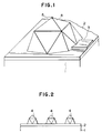
- FIG. 1 A first example is shown in Fig. 1. It exhibits an appearance provided with a single crystal probe having a thin film (insulating film) 2, an electrode 3 on a substrate 1 and an information reading portion 5 at the tip.
- Fig. 2 is a side view of the embodiment in which the single crystal probe 4 formed according to the present invention is provided in a plural number.
- FIG. 3 Another embodiment of the present invention using the microprobe as the current detecting probe is shown in a plan view in Fig. 3.
- a single crystal probe 4 having an apex portion surrounded by specific facets is provided on a substrate (not shown in Fig. 3).
- a source electrode 32, a gate electrode 31, a drain electrode 33 and a thin film resistance 35 are provided in the vicinity of the single crystal probe 4.
- the probe current detected by the probe 4 is on the order of 10 ⁇ 9A, but a probe current on the order of 10 ⁇ 7A can be obtained by amplification with the MOS transistor 34.
- the S/N ratio can be improved by far greater as compared with the case where the probe current is amplified after being led out of the substrate.
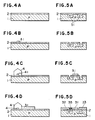
- Fig. 4 is a sectional view showing the first preparation step cut along the line A-A in Fig. 3.
- Fig. 5 is a sectional view showing the first preparation step cut along the line B-B in Fig. 3.
- the microprobe of this embodiment has a different material 41 and a single crystal probe 4 comprising tungsten (W) formed on the basis of the different material 41 provided on the silicon oxide (SiO2) film 2 formed on the silicon substrate 1. Further, in the vicinity of the single crystal probe 4, a MOS transistor 34 for amplifying the probe current is provided.
- the MOS transistor 34 has a gate electrode 31 comprising aluminum, a source electrode 32 and a drain electrode 33 comprising aluminum (Al), and a thin film resistance 35 comprising a material such as luthenium, etc.
- the materials for the respective electrodes are not limited to those mentioned above, but they may also comprise a metal such as Al, Au, Cu, Ag, Cr, W, etc., mixtures of semiconductors such as silicide, etc. with such a metal.
- the different material chip 41 used in this embodiment had a size of 1 »m square, and as the result of preparation according to the preparation method as described below, a very fine single crystal probe 4 having a tip diameter of 0.1 »m order or less was obtained.
- a p-type silicon semiconductor substrate 1 was prepared, and on its one main surface was formed a silicon oxide (SiO2) film 2.
- a silicon oxide (SiO2) film 2 In the region for forming the MOS transistor 34, n+ diffusion layer 51 having antimony (Sb) diffused therein which become respectively source and drain regions is formed.
- Fig. 4B on the silicon oxide film 2 was deposited by the vacuum vapor deposition method, which was then worked by the photolithographic technique to form a different material 41 of 1 »m square.
- openings are formed in layer 2.
- the substrate 1 was then placed in a reaction furnace heated to 500 °C, and the gas mixture of WF6 gas and H2 gas was permitted to flow under reduced pressure of 1 Torr at flow rates of 75 cc/min. and 10 cc/min., respectively.
- the different material chip 41 comprising silicon has by far greater nucleation density as compared with the silicon oxide film 2, tungsten crystal will grow around the different material chip 41 as the center.
- the different material chip 41 is sufficiently fine to the extent that only a single nucleus can grow, a single nucleus was formed on the different material chip 41, and further the nucleus grew while maintaining the single crystal structure, resulting in formation of a single crystal probe 4 (Fig. 4C).
- a gate electrode 31 was formed according to the sputtering method (Fig. 4D, Fig. 5C). Next, thin film resistance materials such as aluminum and ruthenium were vapor deposited and worked by use of the photolithographic technique to form the source electrode 32, the drain electrode 33, the thin film resistance 35 of the MOS transistor 34, thus obtaining a microprobe having the MOS transistor 34 for amplification shown in Fig. 3 and Fig. 5D.
- the above gate electrode 31 may be also made a polycrystalline gate electrode.
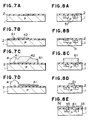
- FIG. 6 through Fig. 8 are drawings for illustration of one embodiment of a microprobe and its preparation of the present invention, Figs. 7A - 7D showing sectional views in the principal preparation steps cut along the line A-A in Fig. 6, Figs. 8A - 8D sectional view in the principal steps along the line B-B in Fig. 6, and Fig. 6 a plan view of the completed microprobe.
- the microprobe of this embodiment has different material chips 41 and 42 and a single crystal probe 4 comprising tungsten (W) formed on the basis of the different material chip 41 provided on the silicon oxide (SiO2) film 2 formed on the silicon substrate 1, and further in the vicinity of the single crystal probe 4 is provided the MOS transistor 34 for amplifying the probe current.
- the MOS transistor 34 has a polycrystalline gate electrode 61 comprising tungsten formed on the basis of the different material chip 42, a source electrode 32 and a drain electrode 33 comprising aluminum (A1), and a thin film resistance 35 comprising a material such as ruthenium, etc.
- the different material chip 41 used in this embodiment has a size of 1 »m square and, as the result of preparation according to the preparation method as described below, a very fine single probe 4 having a tip diameter of 0.1 »m order or less was obtained.
- a p-type silicon semiconductor substrate 1 was prepared, and a silicon oxide (SiO2) film 2 was formed on its one principal surface.
- n+ diffused layer 51 having antimony (Sb) diffused therein which functions respectively as the source and drain regions is formed.
- silicon oxide film 2 silicon was deposited by the vacuum vapor deposition method and worked by use of the photolithographic technique to form a different material chip 41 of 1 »m square and a different material chip 42 extending in the longer direction of the substrate 1.
- the distance between the different material chip 41 and the different material chip 42 was made about 50 »m which was the same as the radius of the single crystal to be formed.
- the substrate 1 was placed in a reaction furnace heated to 500 °C, and a gas mixture of WF6 gas and H2 gas was permitted to flow under a reduced pressure of 1 Torr at the flow rates of 75 cc/min. and 10 cc/min., respectively.
- a gas mixture of WF6 gas and H2 gas was permitted to flow under a reduced pressure of 1 Torr at the flow rates of 75 cc/min. and 10 cc/min., respectively.
- the different material chip 41 is sufficiently fine to the extent that only a single crystal can grow, a single nucleus is formed on the different material chip 41, and further this nucleus grows while maintaining the single crystal structure, resulting in formation of the single crystal probe 4.
- the different material chip 42 is not so fine as to permit only single crystal to grow, a polycrystalline gate electrode 61 comprising tungsten was grown on the different material chip 42 (Fig. 7C, Fig. 8C).
- the polycrystalline gate electrode 61 was worked by use of the photolithographic technique to obtain a polycrystalline gate electrode 61 having a predetermined width.
- thin film resistance materials such as aluminum (Al) and ruthenium were vapor deposited and worked by use of the photolithograhic technique to form the source electrode 32, the drain electrode 33 and the thin film resistance 35 for the MOS transistor, thus obtaining a microprobe having the MOS transistor 34 for initial stage amplification in Fig. 6 and Fig. 8E.
- the single crystal probe 4 comprising tungsten is formed on the silicon oxide film 2 by use of silicon as the different material chip 41, but the material for the single crystal probe is not limited thereto.
- the material for the single crystal probe is not limited thereto.
- the probe electrode as described above can be formed in a plural number.
- Fig. 9 illustrates schematically the plan view having the multi-probe electrode corresponding to Fig. 3 and Fig. 10 illustrates schematically the plan view having the multi-probe electrode corresponding to Fig. 6.
- the numeral 2 represents a thin film formed on a substrate; 4a and 4b, single crystal probes; 31a and 31b, gate electrodes; 32a and 32b, source electrodes; 33a ad 33b, drain electrodes; 34a and 34b, MOS transistors; 35a and 35b, thin film resistors.
- the micro-multi-probe of this embodiment has different material chips 41a, 41b and 42a, 42b and single crystal probes 4a, 4b comprising tungsten (W) formed on the basis of the different material 41a, 41b provided on the silicon oxide (SiO2) film 2 formed on the silicon substrate, and further in the vicinity of the single crystal probes 4a, 4b are provided MOS transistors 34a, 34b for amplifying the probe current.
- the MOS transistor 34 has polycrystalline gate electrodes 61a, 61b comprising tungsten formed on the basis of the different material chips 42a, 42b, source electrodes 32a, 32b and drain electrodes 33a, 33b comprising aluminum (Al), and thin film resistances 35a, 35b comprising a material such as ruthenium, etc.
- the size of the different material chip 41 was set at 1 »m square, but it is possible to form a different material chip 41 of up to several »m, or below 1 »m, by working by use of the ultra-fine working technique using X-ray, electron beam, ion beam after deposition of the different material by use of the sputtering method, the CVD method, the vacuum vapor deposition method, etc., and by controlling accurately the process conditions, a fine single probe 4 having a radius of curvature of the tip of a molecular or atomic level can be obtained.
- Fig. 11 is a sectional view showing the structure of another embodiment of the microprobe of the present invention.
- a different material chip 41 was directly provided on the substrate 1 and a single probe 4 was grown thereon.
- the different material chip 41 selected should have good adhesiveness to the substrate 1 and also have sufficiently greater nucleation density as compared with the substrate 1.
- ions may be injected selectively into a part of the substrate 1 by use of the converged ion beam technique, thereby forming a layer with great nucleation density at that portion.
- Fig. 12 is a sectional view showing another embodiment of the microprobe of the present invention.
- This embodiment has the central part of the substrate 1 protruded, and a single crystal probe 4 is formed on the protruded portion. According to this embodiment, the height of the probe can be controlled by the shape of the substrate 1.
- the present invention is not limited to the embodiments as described above, but various modifications may be possible.
- the substrate when a single crystal probe is directly provided on the substrate, the substrate is not limited to a single crystal, provided that the condition of having sufficiently smaller nucleation density as compared with the different material, and a polycrystalline or amorphous material may be also available.
- the substrate when a single crystal probe is formed on a thin film with sufficiently small nucleation density, the substrate may be either a silicon single crystal wafer or a quartz substrate, or further a substrate of metal, semiconductor, magnetic material, piezoelectric material, insulating material, etc. may be used.
- the first stage amplifier is not limited to MOS transistor, but a bipolar transistor may be used, and its structure and preparation method can be suitably selected.
- the first stage amplifier may be previously prepared before formation of the single crystal probe, or alternatively it may be prepared after formation of the single crystal probe. After completion of the crystal growth of the single crystal probe, working may be further applied thereon by way of the electrical field polishing method or the plasma etching method.
- the single crystal probe 4 shown in Fig. 1 can be also formed according to other methods than the methods as shown in Fig. 4 and Fig. 7 as described above.
- an insulating layer having an opening with a part of the single crystal substrate being exposed is provided on a single crystal substrate and, with the above insulating layer as the mask, an apex portion surrounded by the facets having specific plane distances and comprising specific crystal faces is subjected to selective epitaxial growth from the above opening, thereby growing a single crystal.
- Selective epitaxial growth is made to occur on a single crystal substrate (a material with great nucleation factor) by utilizing the difference in factors influencing nucleation under the crystal growth process between the materials such as surface energy, adhesion coefficient, surface diffusion speed, etc.
- epitaxial growth is permitted to occur only from the single crystal substrate surface exposed at the opening on the mask.
- the mask surface is a non-nucleation surface, generation of such stable nucleus is inhibited and crystal growth occurs selectively only from the single crystal substrate at the mask opening.
- Figs. 13A - 13D The crystal growth process during that period is described by referring to Figs. 13A - 13D.
- Fig. 13A crystal formation treatment is applied on the single crystal substrate 1 of a desired crystal direction provided with an opening 133 to have the surface of the single crystal substrate 1 exposed, by the crystal growth method as described above and under the growth conditions where no stable nucleus of crystal is generated on the surface of the mask 2 (specifically the conditions as shown later in Table 1).
- the crystal will grow epitaxially only from the single crystal substrate surface at the bottom of the opening 133 to embed gradually the opening 133 (Fig. 13 (b)).
- the crystal 134 under growth inherits the information concerning crystallinity such as crystal direction, etc. of the single crystal substrate.
- the crystal 134 will at least grow over the mask 2 in the form covering the surface of the mask 2 (overgrowth) to become a single crystal 4 provided with an external form having facets (Fig. 13C).
- the external form of the single crystal by the facets will grow into a large single crystal 4 as shown in Fig. 13B as accompanied with the increase of surface area of the single crystal 4.
- the single crystal 4 has the same crystal direction as the single crystal substrate 1, if its material is the same as the substrate single crystal 1, or if it has the same symmetry and approximate lattice constants even though the material is different. Accordingly, even when a plural number of crystals may be formed on the substrate, they will all have the external form of the same crystal direction.
- an insulating film 2 comprising a silicon oxide (SiO2) film with a thickness of about 2000 ⁇ is formed by thermal oxidation (Fig. 14A and Fig. 15B), and then an opening 133 (diameter 1.2 »m) is formed in a matrix with intervals of 50 »m is formed by use of the photolithographic technique (Fig. 14B and Fig. 15B).
- n+ type region 51 is formed by use of such means as impurity diffusion or ion implantation onto the p-type silicon single crystal substrate 1 (Fig. 14C and Fig. 15C). By this, a p-n junction is formed.
- a Si single crystal of about 15 »m of grain size having an apex portion surrounded by the facets as shown in Fig. 16 was formed in all of the openings as the center (Fig. 14D). Also, as shown in Fig. 15C, after formation of the p-n junction, the source electrode 32, the thin film resistance 35, the gate electrode 31 and the drain electrode 33 were formed according to the sputtering method to obtain Fig. 15D.
- electrode materials Al, etc. and for thin film resistance, materials such as ruthenium can be used, respectively.
- a current detecting microprobe 4 having the MOS transistor 34 for first stage amplification of the detected current as shown in Fig. 3, Fig. 14E, Fig. 15D could be prepared.
- the single crystal substrate may be also a substrate of a metal, a magnetic material, a piezoelectric material, an insulating material etc.
- the electrode materials, the insulating films, the thin film resistance in the present invention are not limited to this embodiment.
- the method for crystal formation treatment include, for example, the CVD method, the LPE method, the MOCVD method, etc., but of course other methods than these may be employed.
- the material for crystal growth may be either the same as or different from the material of the single crystal substrate.
- the material for crystal growth can be made Ge, Si, GaAs, GaAlAs or other compound semiconductors.
- the material for crystal growth can be made Ge, Si, GaAs, GaAlAs and other compound semiconductors.
- the single crystal as described above takes a growth form surrounded by facets comprising specific crystal faces due to anisotropy in growth speed.
- the crystal faces forming the facets are generally faces with slow growth speed, the growth speed is sensitive to the change in environmental phase during growth and its anisotropy is also great, and consequently the growth form of the single crystal depends on the growth method and the growth conditions. Accordingly, if a single crystal substrate having a suitable plane direction corresponding to the crystal to be grown is selected, a mask is formed thereon and a crystal formation treatment is applied thereon by selecting suitable growth method and suitable growth conditions, a single crystal having an apex portion surrounded by facets can be obtained.
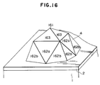
- Fig. 16 is a perspective view of the single crystal thus formed.
- the single crystal has each facets comprising four (111) faces 162a, eight faces 162b and high dimensional crystal faces 163 between the (311) and (411), and forms an apex portion 161 by the 4 triangular faces 163. Since the facet face 163 is a crystallographical crystal face, the top of the apex portion 161 is provided in principle with a sharpness of atomic level.
- the microprobe of the present invention has such stable structure and the improvement of its performance is obtained by forming the single crystal having a sharp apex portion at a desired position with good controllability.
- the single crystal can be grown to an external form by the facets with the apex portion being surrounded by the (111) faces.
- Fig. 17 is a block diagram showing the constitution of an example of a high density recording-reproducing device by use of the microprobe of the present invention.
- the high density recording-reproducing device writes the data by forming selectively low resistance portion (ON state) by applying a writing voltage between the both ends of the recording layer which has become the high resistance state (OFF state) under the initial state, and performs reproduction of the data by detecting the tunnel current from the probe by applying a voltage smaller than the switching threshold voltage during reproduction.
- the recording medium 184 comprises a substrate 181, a substrate electrode 182 and a recording layer 183, and is placed and fixed on a pedestal portion 185.
- the coarse adjustment mechanism 179 is provided for coarse adjustment control of the position in the vertical direction of the recording medium 184 in order to maintain the distance between the recording medium 184 and the single crystal probe 4 at a certain value, and is driven by the coarse adjustment driving circuit 178.
- Below the coarse adjustment mechanism is further provided an XY state 180, which can move the position of the recording medium 184 in the XY direction.
- the pulse power source 174 is provided for applying pulse voltage for recording/erazing between the single crystal probe electrode 4 and the substrate electrode 182.
- the probe current amplifier 177 amplifies the probe current at the single crystal probe 4 to deliver it to the servo circuit 176, and the servo circuit 176 controls movement in the vertical direction of the fine adjustment control mechanism 175 so that the current from the probe current amplifier 177 may become a desired value.
- the fine adjustment mechanism 175 is controlled in movement in the XY direction by the XY scanning driving circuit 173. Each circuit is controlled comprehensively by a microcomputer 172, and the processing information in the microcomputer 172 is displayed on the displaying device 171.
- the single crystal microprobe 4 prepared by the above method has very fine tip diameter, and is suitable for pracitcal use.
- the microprobe 4 Since the microprobe 4 has a MOS transistor 34 for initial stage amplification on the substrate, a probe current greater by 2 digits as compared with the probe current obtained from conventional probe can be obtained to improve the S/N ratio.
- Fig. 18 is a block diagram showing the constitution of an example of the high density recording-reproducing device when the probe shown in Fig. 17 is used multiwise.
- the two probes 4a, 4b can perform recording and reproduction independently.
- the high density recording medium 184 as mentioned above can be made of a materials having memory-switching phenomenon (electric memory effect) in the current-voltage characteristic.
- dye having suitable ⁇ electron system for the present invention there may be included, for example, dyes having porphyrine skelton such as phthalocyanine, tetraphenylporphyrine, etc., azulene type dyes having squarilium group and croconic methine group as the binding group, cyanine analogue type dyes having two hetero-atom containing heterocyclic rings such as quinoline, benzothiazole, benzoxazole, etc.
- cyanine dyes fused polycyclic aromatic such as anthracene and pyrene
- chain compounds formed by polymerisation of aromatic or heterocyclic ring compounds polymers of diacetylene groups, tetraquinodimethane or tetrathiafluvalene derivatives, analogues thereof and charge transfer complexes thereof, and further metal complex compounds such as ferrocene, trisbipyridyl ruthenium complex, etc.
- a monomolecular film of an organic compound having hydrophobic site and hydrophilic site in one molecule or a built-up film thereof can be easily formed on a substrate, and an organic ultra-thin film which is uniform and homogeneous over a large area can be stably supplied.
- the LB method is a method to prepare a monomolecular film or a built-up film thereof by utilizing the fact that, in a molecule with a structure having hydrophilic site and hydrophobic site within a molecule, when balance between the both (amphiphilic balance) is adequately maintained, the molecules form a monomolecular layer on the water surface with the hydrophilic groups directed downward.
- hydrophobic groups generally known widely such as saturated and unsaturated hydrocarbon groups or fused polycyclic aromatic groups and chain polycyclic phenyl groups, etc. These constitute the hydrophobic portion either individually or as a combination of a plurality thereof.
- hydrophilic groups such as carboxyl group, ester group, acid amide group, imide group, hydroxy group, further amino groups (primary, secondary, tertiary and quaternary), etc. These also individually or in combination constitute the hydrophilic portion of the above molecule.
- a dye molecule having these hydrophilic and hydrophobic groups with good balance, and a ⁇ electron system having adequate size can form a monomolecular film on the water surface to be an extremely suitable material for the present invention.
- R1 corresponds to the group having the ⁇ electron level as mentioned above, and is a long chain alkyl group introduced for making formation of monomolecular film on the water surface easier, with its carbon number n being preferably 5 ⁇ n ⁇ 30.
- R is introduced for making formation of monomolecular film easier, and is not limited to the substituents mentioned here.
- R1 - R4, and R correspond to the group having the ⁇ electron level as mentioned above.
- X is a hydrophilic group, and generally -COOH is used, but also -OH, -CONH2 can be used.
- dye materials suitable for the LB method are suitable for the present invention.
- biological materials e.g. bacteriorhodopsin or Cytochrome C
- PBLG synthetic polypeptides
- the substrate for supporting the material having the electric memory effect as mentioned in the above items (1) to (4) it is required to have the character as an electrode, but a conductor having a conductivity of 10 ⁇ 6 (ohm/cm) is all available. More specifically, there may be included a large number materials, including metal plates of Au, Pt, Pd, Ag, Al, In, Sn, Pb, W, etc. or alloys of these, or glass, ceramics, plastic materials having these metals or alloys vapor deposited thereon, or Si (crystalline, amorphous) or graphite and further electroconductive oxides such as ITO.
- a substrate electrode 182 comprising gold (Au), on which was further formed an LB film of squarilium-bis-6-octylazulene (hereinafter abbreviated as SOAZ) as the recording layer 183.
- SOAZ squarilium-bis-6-octylazulene
- chromium (Cr) was deposited thereon as the subbing layer to a thickness of 50 ⁇ according to the vacuum vapor deposition method, and further gold (Au) was vapor deposited to 400 ⁇ according to the same method to form a substrate electrode 182.
- a chloroform solution containing SOAZ at a concentration of 0.2 mg/ml dissolved therein was spread on an aqueous phase of 20°C and a monomolecular film was formed on the water surface.
- the surface pressure of such monomolecular film was enhanced to 20 mN/m, and further while maintaining this pressure constantly, the above electrode substrate was dipped at a speed of 5 mm/min. so as to transverse the water surface, and further withdrawn to build up two-layers Y-type monomolecular films.
- 8 layers of built-up films were formed on the substrate 181 to prepare an LB film of SOAZ.
- the device of the MIM structure by use of the LB film as the insulator exhibits the current-voltage characteristics as shown in Fig. 19 and Fig. 20, having the memory-switching characteristic. More specifically, as shown in Fig. 17 and Fig. 18, the recording current can be passed through the recording layer 183 by the current applied between the substrate electrode 182 and the probes 4a, 4b, whereby the high resistance state (OFF state) at the initial state can be changed to the low resistance state (ON state). As shown in Fig. 20, when under the OFF state, substantially no probe current will flow even when the probe voltage may be applied during reproduction, while under the ON state, the probe current changing linearlly at around -1 V to 1 V will flow. From this fact, ON/OFF of the recording layer 183 can be detected.
- two probe electrodes shown by 4a, 4b in Fig. 18 are utilized separately for positional detection and for recording-reproduction.
- the numeral 211 and 212 denote probe electrodes to be used to recording-reproduction and positional detection, respectively, and the distance between these two probe electrodes can be minutely controlled by the minute control mechanism 213 between the prove electrodes by use of a piezoelectric device, but generally maintained at a constant interval.
- 177 is a probe current amplifier, and 176 is a servo circuit for controlling the fine adjustment mechanisms 175a, 175b by use of piezoelectric devices so that the probe current may become constant.
- 174 is a pulse power source for applying pulse voltage between the probe electrode 211 for recording and reproduction and the substrate electrode 182.
- the servo circuit 176 controls the HOLD circuit so as to be ON so that the output voltage may become constnat during application of the voltage.
- 173 is an XY scanning driving circuit for moving a pair of probe electrodes 211, 212 in the XY direction. 178 and 179 are used for coarse adjustment control of the distance between the probe electrodes 211, 212, and the recording medium 184 so that a probe current of about 10 ⁇ 9 A may be obtained, or for taking a great relative displacement in the XY direction between the probe electrode and the substrate (outside of the fine adjustment control mechanism).
- Z-direction fine adjustment control range 0.1 nm - 1 »m
- Z-direction coarse adjustment control range 10 nm - 10 mm
- XY-direction scanning range 0.1 nm - 1 »m
- XY-direction coarse adjustment control range 10 nm - 10 mm
- the positional detection method of the present invention utilizes the fact that tunnel current will flow when the electroconductive probe (probe electrode) and an electroconductive substance are made to approach to a distance of about 1 nm while applying voltage therebetween, similarly as in recording and reproduction of information. Since tunnel current depends on the work function on the conductor surface, informations about various surface electron states can be read.
- regular atomic arrangement or such regular atomic arrangement for a recording medium having an original point which becomes the standard formed as desired, or a positional coordinate system based on the standard original point is introduced to perform positional detection by detecting the characteristic change in tunnel current corresponding to such positional coordinate system, and at the same time recording or reproduction position on the recording medium exhibiting the relative positional relationship to such positional coordinate system are specified based on such positional detection result, simultaneously with positional control of the probe electrode on such recording and reproduction position.
- Fig. 22 shows a schematic illustration of the positional relationship between the coordinate axis and the recording position.
- the position information (A - I) as the scale on the coordinate axis is always given by relative positional relationship (A - A′, etc.) with the recording positions (A′ - I′).
- the recording positions of A′ - I′ can be necessarily specified.
- the respective points (scale) on the coordinate axis are not necessarily required to take one single arrangement relative to the recording positions (for example, there are a plural number of recording positions corresponding to the positional information A exist, such as A ⁇ , A′′′, in addition to A′), but a single correspondence (1:1 correspondence) is preferred for precision.
- the coordinate axis is not required to be one, but a plurality thereof may be used, and also it is not required to be one-dimensional but also two-dimensional (in network).
- the recording positions are also arranged two-dimensionally.
- the coordinate axis as the positional detection system to be used in the present invention is formed by use of a regular atomic arrangement and/or the standard point formed as desired.
- regular atomic arrangement an electroconductive material of which the distance between lattices is known, namely various metals or graphite single crystals, etc. can be utilized.
- the tunnel current utilized in the present invention is as great as about nA, the above electroconductive material may have an electrical field ratio of 10 ⁇ 10 ( ⁇ cm ⁇ 1), or higher, and therefore a single crystal of a semiconductor such as silicon, etc. can be also used. Among them, as a typical example is considered a metal sample.
- J T ( ⁇ V/2 ⁇ z)exp(-2Z/ ⁇ ) (1)
- the state of atomic arrangement is any desired direction with a certain lattice point on any desired crystal face is self-explanatory, and the periodical change in tunnel current obtained can be sufficiently predicted for the case of scanning the probe electrode in such direction.
- the probe electrode will move along the atomic arrangement of the sample.
- the atomic arrangement is regarded as the coordinate axis
- the probe electrode will move on the coordinate axis.
- the probe electrode on the coordinate axis can be moved in a certain direction to a position with a certain distance apart threrefrom and the destination of movement is a region capable of recording and reproduction, and then recording and reproduction become possible at the positions corresponding at 1:1 to the respective points on the coordinate axis.
- the probe electrode is not necessarily moved between the coordinate axis and the recording region.
- the position of the probe electrode in the recording region namely the recording position can be determined corresponding singly to the coordinate axis utilizing the crystal lattice of the metal sample.
- the recording medium of the present invention is constituted of a combination of the electric memory material as described above and its supporting substrate (electrode), and when atomic arrangement is used as the coordinate axis, the atomic arrangement of such electric memory material itself is frequently inferior in its regularity and not preferably utilized as the coordinate axis. Accordingly, it is desirable to use a material having regular atomic arrangement such as a metal, a crystalline Si, graphite, etc. as the substrate and then, by making a part thereof undeposited with the electric memory material, utilize the substrate atomic arrangement at such site as the coordinate axis.
- Fig. 23 shows a constitutional diagram of a recording medium.
- a P-type Si wafer with the (111) face exposed of 1/2 inch indiameter (B doped, 0.3 mm thickness) was used as the substrate 181.
- the substrate is cut at the B-B′ line for the purpose of setting the recording-reproducing device on the X-Y stage 180 in a constant direction.
- the B-B′ line is substantially in parallel to the ( 2 11) direction of the Si crystal.
- the position of 1 mm from the center of B-B′ toward the substrate center is etched at 1 »m square to the depth of 0.2 »m to prepare the standard original point (coarse) 231.
- the method for preparing such standard original point (coarse) is shown below.
- PMMA polymethyl methacrylate
- OEBR-1000 trade name OEBR-1000, produced by Tokyo Oka Kogyo K.K.
- OEBR-1000 an electron beam resist to a thickness of 1 »m
- an electron beam was projected to draw an image of a size of 1 »m square at an acceleration voltage of 20 keV and a beam diameter of 0.1 »m diameter.
- a developer suitable for this purpose the electron-beam-irradiated portion was dissolved.
- a gas mixture of CF4 and H2 was employed to effect sputter etching under a pressure of 3 Pa and a discharging voltage of 100 W for 20 minutes. The etching depth at that time was 0.2 »m.
- PMMA was dissolved by use of methyl ethyl ketone.
- masking was effected in the vicinity of the standard original point (coarse) 231, followed by deposition of Cr as th subbing layer to a thickness of 50 ⁇ according to the vacuum vapor deposition method, and further Au was deposited to 400 ⁇ by the same method to provide a substrate electrode 182.
- an LB film (8 layers) of squarilium-bis-6-octylazulene (hereinafter abbreviated as SOAZ) similarly as described above to provide a recording layer 101. That is, a benzene solution containing SOAZ at a concentration of 0.2 mg/ml dissolved therein is first spread on an aqueous phase of 20 °C to form a monomolecular film on the water surface. After evaporation of the solvent to enhance the surface pressure to 20 mN/m, and further while maintaining this pressure constantly, the above substrate was dipped and withdrawn gently at a speed of 3 mm/min. in the direction transversing the water surface repeatedly, thereby forming 8-layer built-up films of SOAZ monomolecular film on the substrate electrode 104.
- SOAZ squarilium-bis-6-octylazulene
- the recording medium 184 having the recording layer 183 of built-up 8 SOAZ layers was placed on the X-Y stage 180 with the cutting B-B′ of the substrate set in a predetermined direction.
- the probe electrode 212 for positional detection was moved and, after application of a probe voltage of 0.6 V between the probe electrode for positional detection and the Si substrate 181, the X-direction of the X-Y direction fine adjustment mechanisms 173, 175a being tentatively adjusted in the direction substantially in parallel to B-B′, scanning was effected over a length of 1 »m.
- scanning was also effected in the Y direction (the direction perpendicular to the X-direction) over 1 »m.
- Measurement of the surface state was repeated by varying the manner of taking the X-Y coordinate axes at this time, the arrangement pitches of Si atoms obtained were controlled to take the values most approximate to 6.65 ⁇ and 3.84 ⁇ , respectively,
- X-axis of the X-Y fine adjustment mechanism coincides with the ( 2 11) direction of the Si substrate, and the Y-axis with the (01 1 ) direction.
- the X-Y direction of the coarse adjustment mechanism was controlled so as to coincide with the X-Y direction of the fine adjustment mechanism controlled within the control error range of the coarse adjustment mechanism.
- the position of the standard original point (coarse) 231 was detected by scanning the probe electrodes for positional detection by use of the coarse adjustment methanism.
- the lattice point of Si was detected.
- the probe electrode for positional detection 212 was scanned in the X-direction [( 2 11) direction].
- the directional control correction and confirmation of the positional coordinate (lattice pitch) were effected.
- the probe electrode 211 for recording-reproduction has also moved on the recording 183.
- the distance between the both probe electrodes was 3 mm in the direction of Y-axis. Recording of a desired information was performed by use of such probe for recording-reproduction 211, but prior to practical recording, the standard original point (fine) 242 was provided at the recording position (the point C′ in Fig. 24) corresponding to the positional coordinate original point 241.
- Such standard original point (fine) was formed by utilizing the electric memory effect of the recording layer 183. More specifically, between the probe electrode for recording-reproduction 211 and the Au electrode 182 was applied a probe voltage of 1.0 V, and the distance (Z) between the probe electrode for recording and reproduction 211 and the recording layer 183 was controlled by use of the fine adjustment mechanism 175b so that the probe current Ip may be 10 ⁇ 9A. With the probe electrode for recording-reproduction 211 on the + side and the Au electrode 182 on the - side, a rectangular pulse voltage (18V, 0.1 »s) higher than the threshold voltage (Vth) for ON state at which the electric memory material (SOAZ, 8 layers of LB films) was changed to low resistance state (ON state) to cause the ON state to occur.
- Vth threshold voltage
- the recording-reproduction method was as described above.
- the probe current Ip was measured by applying a probe voltage of 1.0 V between the probe electrode for recording-reproduction 211 and the Au electrode 182, while maintaining the distance (Z) between the probe electrode for recording-reproduction and the recording layer 183, a current of about 0.5 mA was found to flow, whereby the ON state was confirmed to exist.
- the standard original point (fine) 242 was set. During this operation, by bringing the recording region of 10 nm square to ON state, the positional information as the original point concerning the standard point (fine) 242 was prevented from confused reproduction with the recording information written later (Fig. 24), but the shape of the standard original point (fine) 242 is not limited to the shape of this embodiment at all.
- the probe electrode for positional detection 212 was scanned with respect to the X-Y direction to detect the position of the standard original point (coarse) 231. Based on such standard original point (coarse) 231, the probe electrode 211 for recording-reproduction was scanned by use of fine and coarse adjustment mechanisms to detect the position of the standard original point (fine) 242.
- the probe electrode for positional detection 212 was confirmed to exist on the Si lattice point (positional coordinate original point 241).
- X-Y coordinate system was corrected to control the probe electrode for positional detection 212 so as to coincide with the lattice point.
- scanning was effected in the ( 2 11) direction (X-axis direction) while detecting the position of the Si lattice point.
- the reproduction time at this time could be accelerated by about one digit as compared with the case when a tungsten probe, etc. of the prior art was used.
- the probe electrode 4 in Fig. 17 was prepared according to the selective deposition method (See Fig. 13A - Fig. 13D). As the result, a silicon single crystal 4 with a grain size of about 15 »m having an apex portion surrounded by the facet as shown in Fig. 13D was formed with the center at the opening 133.
- the probe electrode 4 is provided for controlling the distance (Z) from the surface of the recording medium 184, and its distance (Z) is subjected to fine adjustment control by a piezoelectric device so that the current may be constantly maintained. Further, the fine adjustment mechanism is designed so that fine adjustment control may be also possible in the (X,Y) direction within the plane, while maintaining constantly the distance (Z).
- the probe electrode 4 is used for performing relative directional positional detection within the recording medium plane and recording-reproducing-erasing.
- the recording medium 184 is placed on an X-Y stage 180 of high precision, and can be moved to any desired position (X-Y coarse adjustment mechanism).
- the X, Y directions of the coarse adjustment mechanism and the X,Y directions of the fine adjustment mechanism are coincident within the range of an error caused by the difference in precision between the respective adjustment mechanisms.
- Fig. 25A is a plan view of the recording medium used in the present invention, and Fig. 25B a cross-sectional view cut along A-A′ thereof.
- a P-type Si wafer with the (111) face exposed of 1/2 inch in diameter (B doped, 0.3 mm thick) was used as the substrate 181.
- the substrate is cut at the B-B′ point for the purpose of setting the recording-reproducing device on the X-Y stage 180 in a constant direction.
- the B-B′ point is substantially in parallel to the ( 2 11) direction of the Si crystal.
- etching was effected at the position of 1 mm from the center of B-B′ toward the substrate center to 1 »m square and 0.2 »m depth to prepare the standard original point 252 (coarse).
- the method for preparing such standard original point (coarse) is shown below.
- PMMA polymethyl methacrylate
- OEBR-1000 trade name OEBR-1000, produced by Tokyo Oka Kogyo K.K.
- OEBR-1000 an electron beam resist to a thickness of 1 »m
- an electron beam was projected to draw an image of a size of 1 »m square at an acceleration voltage of 20 keV and a beam diameter of 0.1 »m in diameter.
- a developer suitable for this purpose the electron-beam-irradiated portion was dissolved.
- a gas mixture of CF4 and H2 was employed to effect sputter etching under a pressure of 3 Pa and a discharging voltage of 100 W for 20 minutes. The etching depth at that time was 0.2 um.
- PMMA was dissolved by use of methyl ethyl ketone.
- masking was effected in the vicinity of the standard original point (coarse) 252, followed by deposition of Cr as the subbing layer to a thickness of 50 ⁇ according to the vacuum vapor deposition method, and further Au was deposited to 400 ⁇ by the same method to provide a substrate electrode 182.
- a recording layer 183 On the Au electrode was laminated an LB film (4 layers) of squarilium-bis-6-octylazulene (hereinafter abbreviated as SOAZ) to provide a recording layer 183.
- SOAZ squarilium-bis-6-octylazulene
- the method for forming the recording layer is to be described. First, a benzene solution containing SOAZ dissolved at a concentration of 0.2 mg/ml therein was spread on an aqueous phase of 20 °C to form a monomolecular film on the water surface.
- the above substrate was dipped and withdrawn gently at a speed of 3 mm/min in the direction transversing the water surface repeatedly, thereby forming a 4-layer built-up films of SOAZ monomolecular film on the substrate electrode 182.
- the recording-reproduction experiment was practiced by use of the recording medium 184 thus prepared.
- the recording medium 184 having the recording layer 183 of built-up 4 SOAZ layers was placed on the X-Y stage 180 with the cutting B-B′ of the substrate, set in a predetermined direction.
- the probe electrode 4 was moved to the position of about 1 mm inside of the substrate from B-B′ and, after application of a probe voltage of 0.6 V between the probe electrode and the Si substrate 181, the X-direction of the probe fine adjustment mechanisms 175, 176 are tentatively adjusted in the direction substantially in parallel to B-B′, and scanning was effected over a length of 1 »m.
- the X-Y direction of the coarse adjustment mechanism was controlled so as to coincide with the X-Y direction of the fine adjustment mechanism controlled within the control error range of the coarse adjustment mechanism.
- the position of the standard original point (coarse) 252 was detected.
- the standard original point (fine) 251 was provided.
- Such standard original point (fine) is formed by utilizing the electric memory effect of the recording layer 183.
- a prove voltage of 1.0 V was applied between the probe electrode 4 and the Au electrode 182 and the distance (Z) between the probe electrode 4 and the recording layer 183 was controlled by use of the fine adjustment mechanism 175 so that the probe current Ip may be 10 ⁇ 9A.
- the standard original point (fine) 251 was set. During this operation, by bringing the recording region of 10 nm square to an ON state, the positional information concerning the standard point (fine) 251 was prevented from confused reproduction with the recording information written later (Fig. 26), but the shape of the standard original point (fine) 251 is not limited to the shape of this embodiment at all.
- Fig. 26 shows schematically the recording position per one pit on the recording surface 183.
- Such recording was effected according to the same method as in formation of the standard original point (fine) by making ON state and OFF state (high resistance state before recording) on the electric memory material (SOAZ, 4 layers of LB film). (Recording (including reproduction) position corresponds to 261 in Fig. 26).
- the recorded recording medium 1 formed by the above steps was once taken off from the recording-reproduction device, and again set on the X,Y stage 180 to perform the reproduction test.
- the probe electrode was scanned with respect to the X,Y directions by use of a coarse adjustment mechanism to detect the position of the standard original point (coarse) 252.
- the standard original point (coarse) was the basis, the standard original point (fine) 251 was sought out by use of coarse and fine adjustment mechanisms.
- the recorded information was reproduced.
- Fig. 27 shows a constitutional diagram of the recording medium 184 used in this embodiment.
- the substrate 181 a glass substrate (1 mm thickness) subjected to optical polishing of 0.7 x 1.5 cm was used.
- a standard origianl point (coarse) 271 of 1 »m square and 0.1 »m deep was prepared at the position of 1 mm toward the substrate center from the center of B-B′.
- a resist material (trade name: AZ 1350) was coated to a thickness of 1 »m and, after pre-baking, UV-ray exposure by use of a mask, developing and post-baking were effected to form a mask pattern on the glass substrate.
- the glass surface was subjected to dry etching to the depth of 0.1 »m under the conditions of an etching power of 50 W, a gas pressure of 1 Pa and a CF4 gas flow rate of 15 SCCM.
- AZ 1360 of the mask was removed by washing with acetone.
- Such substrate was left to stand in saturated vapor of hexamethyldisilazane to apply the hydrophobic treatment on the surface.
- Cr was deposited as the subbing layer to a thickness of 50 ⁇ according to the vacuum vapor deposition method, and further Au was vapor deposited to 400 ⁇ according to the same method to provide a substrate electrode 182.
- Au electrode was laminated a 10-layer LB film of t-butyl derivative of luthetium diphthalocyanine (LuH(Pc)2) to form a recording layer 183. During this operation, care was taken so that no recording layer 183 was deposited in the vicinity of the standard original point (coarse) 271.
- a second standard original point (fine) 273 was made at the position 1 »m in the Y-axis direction from such first standard original point (fine) 272.
- the method for making such second standard original point (fine) 273 is the same as making the first standard original point (fine), and the shapes of the respective points may also be made different for discrimination between the both, which however is not necessarily required, but there may be made a contrivance so that these points are not confused with the recording information in general.
- the information was recorded at 0.01 »m pitch.
- the standard original point (coarse) 271 is found by scanning the probe electrode with respect to X, Y directions by a coarse adjustment mechanism similarly as in recording, and on the basis of such standard original point (coarse), the first standard original point (fine) 272 was sought out by use of the coarse and fine adjustment mechanisms.
- the second standard original point (fine) 273 was detected, followed by reset of the X, Y coordinate system so that the direction of the line connecting the first and second standard original points (fine) may coincide with the Y-axis direction of the probe electrode scanning system.
- the first standard original point (fine) 272 or the second standard original point (fine) 273 was set so as to become the original point of such X, Y coordinate system in carrying out reproduction of the recorded information.
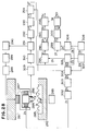
- Fig. 28 shows the constitution of the encoder according to an embodiment of the present invention.
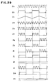
- Fig. 29 and Fig. 30 show the signals obtained in the respective constitutional parts of this embodiments.
- the subject matter 281 and the subject matter 282 are set so that they can be only moved relatively in the lateral direction (left and right direction within the paper plane).
- the subject matter 282 is provided with an electroconductive standard scale 283, and the subject matter 281 with an electroconductive probe 284.
- a bias voltage by the bias power source 285.
- the tip end of the probe 284 and the standard scale 283 are approximated to each other to the extent that tunnel current flows therebetween.
- tunnel current is converted by the current-voltage converting circuit 309 to voltage, which after amplified by the amplifying circuit 310 is subjected to logarithmic conversion by the logarithmic conversion circuit 291 in order to make the output signal proportional to the distance between the probe and the scale.
- the probe 284 vibrates at a vibration number f and an amplitude d in the relative moving direction of the object matter 281 and the object matter 282 by means of the probe vibrating means 286.
- the vibration speed at this time is sufficiently greater than the relative moving speed of the subject matters 281 and 282.
- the probe vibration signal converts the rectangular wave 2a with a vibration number nf outputted from the oscillator 307 to a divided signal 2b in the frequency dividing circuit 304, to a triangular wave (signal 2c) with a vibration number f by the wave form converting circuit 303 and, after amplified by the amplifier 302 applied to the probe vibrating means 286.
- the standard scale may be also vibrated by providing a standard scale vibrating means on the object matter 282.
- the output signal from the logarithmic conversion circuit 291 is detected so that the average interval between the probe and the standard scale may become constant (so that the average value of the detected tunnel current may become constant), and if the detected tunnel current value is deviated from the set value, by use of an average tunnel current value setting circuit 290 which will output the signal so as to correct its difference and further by use of a low pass filter 289 and the amplifying circuit 288, a feed-back group is formed to control the interval between the probe and the standard scale with the probe longitudinal position controlling means 287.
- the cut-off frequency of the low pass filter 289 is selected so that the rapid modulation component of the tunnel current caused to occur by scanning of the standard scale by the probe through vibration in the lateral direction of the prove over the standard scale and changing of the heights of the opposed portions of the standard scale and the probe may be removed, thereby permitting the slow change of the tunnel current by slanting of the standard scale, etc. during relative movement in the lateral direction of the object matter 281 and the object matter 282. Therefore, the probe longitudinal position control means 287 will not follow the tunnel current change by vibration, but performs the longitudinal position control of the probe by following only the tunnel current change through the relative movement of the object matter 281 and 282.
- the modulation component with a frequency of (2p/d)f (p is the standard scale interval) by scanning of the probe over the standard scale.
- the modulation component with a frequency of (2p/d)f appearing in the above tunnel current will cause phase deviation relative to the standard signal (e.g. probe vibration signal). Since one period (phase deviation of 2 ⁇ ) corresponds to the relative laterial deviation between the probe and the standard scale corresponding to one scale of the standard scale, by detecting the phase deviation, the amount of the relative lateral movement of the object matter 281 and the object matter 282 can be detected.
- the modulation component with a frequency of (2p/d)f appearing in the tunnel current is taken out (2d, in the Figure) via the current-voltage conversion circuit 309, the amplification circuit 310, the logarithmic conversion circuit 291, the band-pass filter 292, and after binary conversion to through the binary circuit 293, the signal 2e is obtained.
- the signal 2b having the frequency of the signal 2a from the oscillator 307 divided to 1/n by the frequency dividing circuit 304 as the reference signal, the signal 2e is divided by the gate circuit 294 into the two signals 2f, 2g.
- the signal 2a is divided by the gate circuit 305 into the two signals 2h, 2i with the signal 2b as the reference signal.
- the signals 2f and 2h are inputted into a phase comparator 295, and the phase difference output 2j signal is averaged by an averaging circuit 296 to obtain the signal 2k.
- the signal 2k will change as the signal 3a corresponding to its relative movement amount.
- phase difference becomes 2n ⁇ (n: integer)
- the zero-cross point of the phase difference output signal 2k(3a) is detected by the binary conversion circuit 297 to generate pulses (signal 3b), and the relative phase deviation between the signal 2f and the signal 2h (encoder output signal 3c) can be detected by counting the pulse number by an up-down counter 298.
- the phase deviation directional signal inputted into the counter 298, namely the up-down condition (mark) is determined as follows.
- a signal 2l deviated by 90° in phase relative to the signal 2h is formed.
- the phase difference output signal 2m is averaged by the averaging circuit 300 to obtain the signal 2n.
- the signal 2k when the object matter 281 and the object matter 282 move relatively in the lateral direction, the signal 2n will change as the signal 3d corresponding to its relative movement amount. Further, the signal 3d is converted to binary value by the binary conversion circuit 301 to give a phase deviation directional signal, namely the up-down signal 3e inputted to the up-down counter.
- the up-down counter 298 adds the pulse number. On the contraty, it the up-down signal 3e at the stand-up points is -, the pulse number is detracted.
- the lateral direction relative movement amount of the object matter 281 and the object matter 282 can be detected.
- one period of phase deviation (2 ⁇ ) corresponds to the relative movement amount of one scale of the standard scale. Even if there may be a defect, etc. in the standard scale only a part of the waveform of the signal is disturbed, and the value of phase deviation will be hardly affected thereby. Therefore, the measured value can maintain accurateness even by external disturbance.
- the relative movement amount can be also detected by performing the same signal processing for the signal 2g, 2i.
- the single crystal probe 284 used in the above embodiment (the encoder in Fig. 28) is prepared by use of the method of crystal growth shown in Fig. 13. Shortly speaking, the single crystal probe, as shown in Fig. 16, has each facet comprising four (111) faces 162a, eight faces 162b and a high-dimensional crystal face 163 between (311) and (411), and forms an apex portion 161 with four triangular faces 163.
- an encoder of high performance and high resolving power can be confirmed to be provided, which proved to be advantageous in high speed vibration due to strong resistance to electrical noise, vibration (sound, earthquake, etc.) and high rigidity and is also excellent in aspects of reproducibility of information, stability of the device.
- the microprobe of the present invention is a single crystal probe having a sharp apex portion with a size of atomic level surrounded by facets having specific face directions and comprising specific crystal faces, and also having high rigidity without working distortion, and is therefore very useful in practical application.
- These single crystal probes can be freely selected either singly or in a plural number, and besides, they can be formed at any desired position with good controllability according to the present invention. For this reason, it is possible to make the production method high in yield and yet excellent in productivity at low cost by controlling the process.
- microprobe of the present invention can be applied for broad scope of applications because all of conductors, semiconductors, non-conductors can be selected as the constituent material.
- a microprobe having a curvature of radius of molecular level or atomic level can be obtained with good reproducibility by controlling accurately the production process conditions.
- a draw-out electrode or a current amplifier can be formed in adjacent form.
- the S/N ratio on account of an amplifier adjacent to the single crystal probe can be improved by about 1 to 2 digits as compared with the current amplification of the microprobe of the prior art.
- the preparation steps for providing a draw-out electrode or an amplifier can be easily incorporated in a series of preparation steps of the single crystal probe, and the single crystal probe can be formed without damage.
Landscapes
- Physics & Mathematics (AREA)
- Health & Medical Sciences (AREA)
- General Health & Medical Sciences (AREA)
- General Physics & Mathematics (AREA)
- Nuclear Medicine, Radiotherapy & Molecular Imaging (AREA)
- Radiology & Medical Imaging (AREA)
- Measurement Of Length, Angles, Or The Like Using Electric Or Magnetic Means (AREA)
- Crystals, And After-Treatments Of Crystals (AREA)
Claims (26)
- Verfahren zur Herstellung einer Mikrosonde, umfassend den Schritt, daß auf einem Teil einer Hauptoberfläche eines Trägers (1) oder auf einem Teil eines Dünnfilms (2), der auf einer Hauptoberfläche des Trägers gebildet wurde, ein anderes Material (41) bereitgestellt wird, das eine Keimbildungsdichte besitzt, die ausreichend größer als die Keimbildungsdichte des Trägers oder des Dünnfilms und klein genug ist insofern, daß nur ein einzelner Keim darauf gezüchtet werden kann, und den Schritt, daß ein Einkristall (4) gebildet wird, indem ein einzelner Keim auf dem Material gezüchtet und nachfolgend aus diesem Keim ein Einkristall epitaxial gezüchtet wird, bis sich ein Kopfbereich bildet, der von Kristallflächen umgeben ist.
- Verfahren zur Herstellung einer Mikrosonde, umfassend, daß auf einen Einkristallträger (1) eine Isolationsschicht (2) aufgezogen wird, die eine Öffnung besitzt, so daß ein Teil des Einkristallträgers freigelegt sein kann, und daß ein Einkristall (4), der einen Kopfbereich (5), der von Kristallflächen, die eine bestimmte Ebenenrichtung besitzen, umgeben ist, besitzt und eine bestimmte Kristallfläche umfaßt, durch selektives epitaxiales Züchten aus der genannten Öffnung heraus gezüchtet wird.
- Verfahren zur Herstellung einer Mikrosonde nach Anspruch 2, das weiter den Schritt enthält, daß während des selektiven epitaxialen Züchtens mit einem Gas selektiv dotiert wird.
- Verfahren zur Herstellung einer Mikrosonde nach den Ansprüchen 1, 2 oder 3, das weiter den Schritt umfaßt, daß Abnahmeelektroden in Nachbarschaft des Einkristalls mit dem von den Kristallflächen umgebenen Kopfbereich bereitgestellt werden.
- Mikrosonde, die mit dem Verfahren hergestellt wurde, das in einem der Ansprüche 1 bis 4 offenbart wurde, die einen Einkristall (4) umfaßt, der auf einem Teil einer Hauptoberfläche eines Trägers (1) oder einem Teil eines Dünnfilms (2), der auf einer Hauptoberfläche eines Trägers (1) gebildet wurde, bereitgestellt wird,
weiter dadurch gekennzeichnet, daß der Einkristall ein anderes Material als das des Trägers oder des Dünnfilms umfaßt. - Mikrosonde nach Anspruch 5, dadurch gekennzeichnet, daß der Kristall einen Kopfbereich besitzt, der von Kristallflächen umgeben ist, die eine bestimmte Ebenenrichtung besitzen, und der eine bestimmte Kristallfläche umfaßt.
- Mikrosonde nach Anspruch 6, dadurch gekennzeichnet, daß die Kristallflachen Flächen im Bereich von (411) bis (311) darstellen.
- Mikrosonde nach einem der vorhergehenden Ansprüche, worin der Einkristall ein Wolframeinkristall ist.
- Mikrosonde nach einem der vorhergehenden Ansprüche, dadurch gekennzeichnet, daß der Einkristall ein Siliciumeinkristall ist.
- Mikrosonde nach einem der vorhergehenden Ansprüche, dadurch gekennzeichnet, daß das Kristallmaterial Silicium oder Germanium ist.
- Mikrosonde nach einem der vorhergehenden Ansprüche, die mit einer Elektrodenverdrahtung (3) in Nachbarschaft des Einkristalls versehen ist.
- Mikrosonde nach einem der vorhergehenden Ansprüche, dadurch gekennzeichnet, daß sie einen Verstärker in Nachbarschaft des Einkristalls besitzt.
- Mikrosonde nach Anspruch 12, dadurch gekennzeichnet, daß der Verstärker ein Stromverstärker ist.
- Mikrosonde nach einem der Ansprüche 5 bis 13, dadurch gekennzeichnet, daß eine Vielzahl Einkristalle bereitgestellt wird.
- Mikrosonde nach einem der Ansprüche 5 bis 14, dadurch gekennzeichnet, daß der Träger Siliciumdioxid oder Germanium umfaßt.
- Elektronische Vorrichtung zur Durchführung einer Aufzeichnung und einer Wiedergabe, die eine Mikrosonde, wie sie in einem der Ansprüche 5 bis 15 definiert wurde, ein Aufzeichnungsmaterial (184), das gegenüber der Sondenelektrode (4) bereitgestellt ist, und eine Einrichtung (174) zum Anlegen einer Spannung zwischen der Sondenelektrode und dem Aufzeichnungsmaterial besitzt.
- Vorrichtung nach Anspruch 16, dadurch gekennzeichnet, daß das Aufzeichnungsmaterial (184) eine Positionskoordinatenachse, die als Standard funktioniert, und eine Einrichtung (4, 172 und 173) zum Nachweis der Position auf der Positionskoordinatenachse und zum Durchführen der Aufzeichnung oder der Wiedergabe oder des Löschens der aufgezeichneten Informationen an der Position des Aufzeichnungsmaterials, die der nachgewiesenen Koordinatenposition entspricht, besitzt.
- Vorrichtung nach Anspruch 17, dadurch gekennzeichnet, daß die Positionskoordinatenachse, die als Standard funktioniert, eine Koordinatenachse ist, die auf einer atomaren Anordnung basiert.
- Vorrichtung nach den Ansprüchen 17 oder 18, dadurch gekennzeichnet, daß der Originalpunkt, der als Standard funktioniert, auf wenigstens einem der folgenden bereitgestellt ist: auf der Positionskoordinatenachse, die als Standard funktioniert und an der dementsprechenden Position des Anfzeichnungsmaterials.
- Vorrichtung nach Anspruch 17, 18 oder 19, dadurch gekennzeichnet, daß eine Vielzahl von Positionskoordinatenachsen, die als Standard funktionieren, gebildet wird.
- Vorrichtung nach einem der Ansprüche 17 bis 20, dadurch gekennzeichnet, daß sie eine Vielzahl von Sondenelektroden (4) besitzt, von denen eine Sondenelektrode zum Nachweis der Positionskoordinate verwendet wird und die andere Sondenelektroden zur Aufzeichnung und Wiedergabe verwendet werden.
- Vorrichtung nach einem der Ansprüche 16 bis 21, dadurch gekennzeichnet, daß das Aufzeichnungsmaterial einen elektrischen Speichereffekt besitzt.
- Vorrichtung nach einem der Ansprüche 16 bis 22, dadurch gekennzeichnet, daß das Aufzeichnungsmaterial eine Standardskala, die der Standard innerhalb der Ebene wird, und eine Einrichtung (297) zum Nachweis der relativen Abweichung innerhalb der Ebene des Aufzeichnungsmaterials zwischen der Standardskala und der Sondenelektrode besitzt.
- Vorrichtung nach Anspruch 23, dadurch gekennzeichnet, daß die Standardskala eine Skala ist, die auf einer atomaren Anordnung basiert.
- Elektronische Vorrichtung nach den Ansprüchen 23 oder 24, dadurch gekennzeichnet, daß eine Vielzahl von Standardskalen bereitgestellt ist.
- Elektronische Vorrichtung, umfassend eine elektrisch leitende Standardskala (283), die die Standardskala in Bezug auf die Länge wird, und eine elektrisch leitende Sonde (284) gemäß Definition in einem der Ansprüche 5 bis 15, wobei die Spitze des Kristalls in Nachbarschaft der Standardskalenfläche angeordnet ist, eine Einrichtung (285) zum Anlegen einer Spannung zwischen der Standardskala (283) und der Sonde (284), eine Einrichtung (309) zum Nachweis des Wertes des Tunnelstroms, der zwischen der Standardskala und der Sonde fließt, und zur Ausgabe des Signals, das dem Wert der relativen Bewegung in seitlicher Richtung zwischen Standardskala und Sonde entspricht, basierend auf dem Wert des Tunnelstroms, eine Einrichtung (297) zum Nachweis des Wertes der relativen Bewegung und der relativen Bewegungsrichtung in seitlicher Richtung zwischen der Standardskala und der Sonde, basierend auf dem Ausgabesignal der Signalausgabeeinrichtung, und eine Einrichtung (298) zum Zählen des relativen Abweichungswertes in seitlicher Richtung zwischen der Standardskala und der Sonde aus den Signalen des Wertes der relativen Bewegung in seitlicher Richtung und der relativen Bewegungsrichtung.
Priority Applications (1)
| Application Number | Priority Date | Filing Date | Title |
|---|---|---|---|
| EP93201569A EP0566214B1 (de) | 1987-09-24 | 1988-09-21 | Mikrosonde |
Applications Claiming Priority (12)
| Application Number | Priority Date | Filing Date | Title |
|---|---|---|---|
| JP23750087 | 1987-09-24 | ||
| JP237499/87 | 1987-09-24 | ||
| JP23749987 | 1987-09-24 | ||
| JP237500/87 | 1987-09-24 | ||
| JP318951/87 | 1987-12-18 | ||
| JP31895187 | 1987-12-18 | ||
| JP221403/88 | 1988-09-06 | ||
| JP22140388A JPH0269618A (ja) | 1988-09-06 | 1988-09-06 | エンコーダー |
| JP22223288A JPH0271439A (ja) | 1988-09-07 | 1988-09-07 | 記録再生装置 |
| JP222232/88 | 1988-09-07 | ||
| JP63226420A JP2553661B2 (ja) | 1987-09-24 | 1988-09-12 | 微小プローグ及びその製造方法 |
| JP226420/88 | 1988-09-12 |
Related Child Applications (2)
| Application Number | Title | Priority Date | Filing Date |
|---|---|---|---|
| EP93201569A Division EP0566214B1 (de) | 1987-09-24 | 1988-09-21 | Mikrosonde |
| EP93201569.6 Division-Into | 1988-09-21 |
Publications (3)
| Publication Number | Publication Date |
|---|---|
| EP0309236A2 EP0309236A2 (de) | 1989-03-29 |
| EP0309236A3 EP0309236A3 (de) | 1992-07-01 |
| EP0309236B1 true EP0309236B1 (de) | 1994-07-06 |
Family
ID=27553969
Family Applications (1)
| Application Number | Title | Priority Date | Filing Date |
|---|---|---|---|
| EP88308780A Expired - Lifetime EP0309236B1 (de) | 1987-09-24 | 1988-09-21 | Mikrosonde, deren Herstellung und elektronisches Gerät, das diese Mikrosonde gebraucht |
Country Status (4)
| Country | Link |
|---|---|
| US (1) | US5072116A (de) |
| EP (1) | EP0309236B1 (de) |
| CA (1) | CA1312952C (de) |
| DE (2) | DE3856336T2 (de) |
Families Citing this family (56)
| Publication number | Priority date | Publication date | Assignee | Title |
|---|---|---|---|---|
| US5994698A (en) * | 1987-09-24 | 1999-11-30 | Canon Kabushiki Kaisha | Microprobe, preparation thereof and electronic device by use of said microprobe |
| US5634267A (en) * | 1991-06-04 | 1997-06-03 | Micron Technology, Inc. | Method and apparatus for manufacturing known good semiconductor die |
| US5640762A (en) | 1988-09-30 | 1997-06-24 | Micron Technology, Inc. | Method and apparatus for manufacturing known good semiconductor die |
| EP0363147B1 (de) * | 1988-10-04 | 1996-06-05 | Canon Kabushiki Kaisha | Gerät und Verfahren zur Aufzeichnung und Wiedergabe und Aufzeichnungsmedium für das Aufzeichungs- und Wiedergabeverfahren |
| US5241527A (en) * | 1989-03-16 | 1993-08-31 | Canon Kabushiki Kaisha | Recording and reproducing apparatus and method using a recording layer having a positioning region |
| US4987303A (en) * | 1989-04-07 | 1991-01-22 | Olympus Optical Co., Inc. | Micro-displacement detector device, piezo-actuator provided with the micro-displacement detector device and scanning probe microscope provided with the piezo-actuator |
| JP2775464B2 (ja) * | 1989-04-27 | 1998-07-16 | キヤノン株式会社 | 位置検出装置 |
| GB8910566D0 (en) * | 1989-05-08 | 1989-06-21 | Amersham Int Plc | Imaging apparatus and method |
| JP2686645B2 (ja) * | 1989-05-08 | 1997-12-08 | キヤノン株式会社 | 走査型トンネル電流検出装置 |
| EP0437275B1 (de) * | 1990-01-11 | 1997-08-27 | Canon Kabushiki Kaisha | Mikrosonde, Herstellungsverfahren zur Herstellung derselben und Informations-Eingabe- und/oder Ausgabe-Gerät welches dieselbe verwendet |
| JP2996748B2 (ja) * | 1990-02-09 | 2000-01-11 | キヤノン株式会社 | 位置ずれ検出装置および方法 |
| JP2783646B2 (ja) * | 1990-04-18 | 1998-08-06 | キヤノン株式会社 | 情報記録再生装置 |
| US5171992A (en) * | 1990-10-31 | 1992-12-15 | International Business Machines Corporation | Nanometer scale probe for an atomic force microscope, and method for making same |
| EP0492915B1 (de) * | 1990-12-17 | 1996-09-04 | Canon Kabushiki Kaisha | Freitragende Sonde und Apparat zur Anwendung derselben |
| JP3010318B2 (ja) * | 1991-02-26 | 2000-02-21 | キヤノン株式会社 | 微小プローブ、その製造方法、該プローブを用いた表面観察装置及び情報処理装置 |
| US6219908B1 (en) | 1991-06-04 | 2001-04-24 | Micron Technology, Inc. | Method and apparatus for manufacturing known good semiconductor die |
| US5541525A (en) * | 1991-06-04 | 1996-07-30 | Micron Technology, Inc. | Carrier for testing an unpackaged semiconductor die |
| US5495179A (en) * | 1991-06-04 | 1996-02-27 | Micron Technology, Inc. | Carrier having interchangeable substrate used for testing of semiconductor dies |
| US5585282A (en) * | 1991-06-04 | 1996-12-17 | Micron Technology, Inc. | Process for forming a raised portion on a projecting contact for electrical testing of a semiconductor |
| US6828812B2 (en) * | 1991-06-04 | 2004-12-07 | Micron Technology, Inc. | Test apparatus for testing semiconductor dice including substrate with penetration limiting contacts for making electrical connections |
| US6340894B1 (en) | 1991-06-04 | 2002-01-22 | Micron Technology, Inc. | Semiconductor testing apparatus including substrate with contact members and conductive polymer interconnect |
| US5239260A (en) * | 1991-06-28 | 1993-08-24 | Digital Equipment Corporation | Semiconductor probe and alignment system |
| US5210485A (en) * | 1991-07-26 | 1993-05-11 | International Business Machines Corporation | Probe for wafer burn-in test system |
| US5177439A (en) * | 1991-08-30 | 1993-01-05 | U.S. Philips Corporation | Probe card for testing unencapsulated semiconductor devices |
| US5386720A (en) * | 1992-01-09 | 1995-02-07 | Olympus Optical Co., Ltd. | Integrated AFM sensor |
| KR940001341A (ko) * | 1992-06-29 | 1994-01-11 | 디. 아이. 캐플란 | 전자 장치로의 빠른 전기 접근을 위한 순간 접속법 |
| JPH06187675A (ja) * | 1992-09-25 | 1994-07-08 | Canon Inc | 情報処理装置、及びそれを用いる情報処理方法 |
| US5326428A (en) * | 1993-09-03 | 1994-07-05 | Micron Semiconductor, Inc. | Method for testing semiconductor circuitry for operability and method of forming apparatus for testing semiconductor circuitry for operability |
| US5478779A (en) | 1994-03-07 | 1995-12-26 | Micron Technology, Inc. | Electrically conductive projections and semiconductor processing method of forming same |
| US5483741A (en) * | 1993-09-03 | 1996-01-16 | Micron Technology, Inc. | Method for fabricating a self limiting silicon based interconnect for testing bare semiconductor dice |
| US6337479B1 (en) | 1994-07-28 | 2002-01-08 | Victor B. Kley | Object inspection and/or modification system and method |
| US5751683A (en) | 1995-07-24 | 1998-05-12 | General Nanotechnology, L.L.C. | Nanometer scale data storage device and associated positioning system |
| US6353219B1 (en) | 1994-07-28 | 2002-03-05 | Victor B. Kley | Object inspection and/or modification system and method |
| US6339217B1 (en) | 1995-07-28 | 2002-01-15 | General Nanotechnology Llc | Scanning probe microscope assembly and method for making spectrophotometric, near-field, and scanning probe measurements |
| JPH0862230A (ja) * | 1994-08-24 | 1996-03-08 | Olympus Optical Co Ltd | 集積型spmセンサー |
| US5903161A (en) * | 1995-01-26 | 1999-05-11 | Denki Kagaku Kogyo Kabushiki Kaisha | Electrically conductive rod-shaped single crystal product and assembly for measuring electrical properties employing such product, as well as processes for their production |
| US5532611A (en) * | 1995-05-26 | 1996-07-02 | International Business Machines Corporation | Miniature probe positioning actuator |
| US5869974A (en) * | 1996-04-01 | 1999-02-09 | Micron Technology, Inc. | Micromachined probe card having compliant contact members for testing semiconductor wafers |
| DE19622701A1 (de) * | 1996-06-05 | 1997-12-18 | Fraunhofer Ges Forschung | Mikrobalken mit integrierter Abtast- bzw. Prüfspitze aus Diamant für den Einsatz in Rastersondenmikroskopen |
| JPH10313008A (ja) | 1997-05-13 | 1998-11-24 | Canon Inc | 微細パターンの形成方法及び該微細パターンを有する電気素子 |
| US6752008B1 (en) | 2001-03-08 | 2004-06-22 | General Nanotechnology Llc | Method and apparatus for scanning in scanning probe microscopy and presenting results |
| US6802646B1 (en) | 2001-04-30 | 2004-10-12 | General Nanotechnology Llc | Low-friction moving interfaces in micromachines and nanomachines |
| US6923044B1 (en) | 2001-03-08 | 2005-08-02 | General Nanotechnology Llc | Active cantilever for nanomachining and metrology |
| US7196328B1 (en) | 2001-03-08 | 2007-03-27 | General Nanotechnology Llc | Nanomachining method and apparatus |
| US6787768B1 (en) | 2001-03-08 | 2004-09-07 | General Nanotechnology Llc | Method and apparatus for tool and tip design for nanomachining and measurement |
| EP1196939A4 (de) | 1999-07-01 | 2002-09-18 | Gen Nanotechnology Llc | Vorrichtung und verfahren zur untersuchung und/oder veränderungsobjekt |
| US6931710B2 (en) | 2001-01-30 | 2005-08-23 | General Nanotechnology Llc | Manufacturing of micro-objects such as miniature diamond tool tips |
| US7253407B1 (en) | 2001-03-08 | 2007-08-07 | General Nanotechnology Llc | Active cantilever for nanomachining and metrology |
| JP4310076B2 (ja) * | 2001-05-31 | 2009-08-05 | キヤノン株式会社 | 結晶性薄膜の製造方法 |
| US7053369B1 (en) | 2001-10-19 | 2006-05-30 | Rave Llc | Scan data collection for better overall data accuracy |
| US6813937B2 (en) | 2001-11-28 | 2004-11-09 | General Nanotechnology Llc | Method and apparatus for micromachines, microstructures, nanomachines and nanostructures |
| JP2005538855A (ja) | 2002-09-09 | 2005-12-22 | ジェネラル ナノテクノロジー エルエルシー | 走査型プローブ顕微鏡の流体送達 |
| FR2856184B1 (fr) * | 2003-06-13 | 2008-04-11 | Commissariat Energie Atomique | Dispositif d'enregistrement de donnees comportant des micro-pointes et un support d'enregistrement |
| JP4360863B2 (ja) | 2003-08-07 | 2009-11-11 | Necエレクトロニクス株式会社 | 走査型プローブ検査装置 |
| US20100001229A1 (en) * | 2007-02-27 | 2010-01-07 | Hitachi Chemical Co., Ltd. | Cmp slurry for silicon film |
| US9773889B2 (en) * | 2014-07-18 | 2017-09-26 | Taiwan Semiconductor Manufacturing Company Limited | Method of semiconductor arrangement formation |
Family Cites Families (4)
| Publication number | Priority date | Publication date | Assignee | Title |
|---|---|---|---|---|
| CH643397A5 (de) * | 1979-09-20 | 1984-05-30 | Ibm | Raster-tunnelmikroskop. |
| US4575822A (en) * | 1983-02-15 | 1986-03-11 | The Board Of Trustees Of The Leland Stanford Junior University | Method and means for data storage using tunnel current data readout |
| EP0194323B1 (de) * | 1985-03-07 | 1989-08-02 | International Business Machines Corporation | Tunneleffektabtastungsmikroskop |
| JPS62209302A (ja) * | 1986-03-10 | 1987-09-14 | Shimadzu Corp | 平行移動量検出装置 |
-
1988
- 1988-09-21 DE DE3856336T patent/DE3856336T2/de not_active Expired - Fee Related
- 1988-09-21 CA CA000578008A patent/CA1312952C/en not_active Expired - Fee Related
- 1988-09-21 EP EP88308780A patent/EP0309236B1/de not_active Expired - Lifetime
- 1988-09-21 DE DE3850544T patent/DE3850544T2/de not_active Expired - Lifetime
-
1990
- 1990-11-09 US US07/610,314 patent/US5072116A/en not_active Expired - Lifetime
Also Published As
| Publication number | Publication date |
|---|---|
| DE3856336D1 (de) | 1999-07-01 |
| DE3850544D1 (de) | 1994-08-11 |
| EP0309236A3 (de) | 1992-07-01 |
| US5072116A (en) | 1991-12-10 |
| EP0309236A2 (de) | 1989-03-29 |
| CA1312952C (en) | 1993-01-19 |
| DE3850544T2 (de) | 1994-11-24 |
| DE3856336T2 (de) | 2000-01-27 |
Similar Documents
| Publication | Publication Date | Title |
|---|---|---|
| EP0309236B1 (de) | Mikrosonde, deren Herstellung und elektronisches Gerät, das diese Mikrosonde gebraucht | |
| US5994698A (en) | Microprobe, preparation thereof and electronic device by use of said microprobe | |
| US5482002A (en) | Microprobe, preparation thereof and electronic device by use of said microprobe | |
| EP0416920B1 (de) | Informationsverarbeitungsverfahren und -vorrichtung | |
| US5721721A (en) | Two scanning probes information recording/reproducing system with one probe to detect atomic reference location on a recording medium | |
| JP2741629B2 (ja) | カンチレバー型プローブ、それを用いた走査型トンネル顕微鏡及び情報処理装置 | |
| US5317152A (en) | Cantilever type probe, and scanning tunnel microscope and information processing apparatus employing the same | |
| EP0334677B1 (de) | Informationsaufzeichnungsgerät und Informationsaufzeichnungs-und-wiedergabeverfahren | |
| EP0519745A2 (de) | Aufzeichnungsmedium, Informationsverarbeitungsgerät dafür und Informationslöschverfahren | |
| US5329514A (en) | Information processing apparatus, and electrode substrate and information recording medium used in the apparatus | |
| JPH05284765A (ja) | カンチレバー型変位素子、及びこれを用いたカンチレバー型プローブ、及びこのカンチレバー型プローブを用いた走査型トンネル顕微鏡並びに情報処理装置 | |
| JPH05347439A (ja) | 微小変位素子及びこれを用いた走査型トンネル顕微鏡、情報処理装置 | |
| JP3135779B2 (ja) | 情報処理装置 | |
| EP0553937B1 (de) | Aufzeichnungsgerät und Wiedergabegerät | |
| EP0566214B1 (de) | Mikrosonde | |
| EP0449409A2 (de) | Sonde, Vorrichtung zur Datenverarbeitung in welcher die Sonde benutzt wird und Verfahren zum Gebrauch und zur Herstellung | |
| JPH0271439A (ja) | 記録再生装置 | |
| JPH0760261B2 (ja) | リソグラフイ・マスクの製造方法およびリソグラフイ装置 | |
| JP2553661B2 (ja) | 微小プローグ及びその製造方法 | |
| JPH06333276A (ja) | 記録媒体及びその製造方法、及び該記録媒体を用いた情報処理装置 | |
| JP2670448B2 (ja) | 記録再生装置 | |
| JP3118654B2 (ja) | 情報処理装置及び走査型トンネル電子顕微鏡 | |
| CA2024725C (en) | Information processing method and information processing device | |
| JP2934057B2 (ja) | プローブユニット及びこれを使用する情報記録及び/又は再生装置 | |
| JPH05215509A (ja) | 走査型プローブ顕微鏡とその探針製造方法 |
Legal Events
| Date | Code | Title | Description |
|---|---|---|---|
| PUAI | Public reference made under article 153(3) epc to a published international application that has entered the european phase |
Free format text: ORIGINAL CODE: 0009012 |
|
| AK | Designated contracting states |
Kind code of ref document: A2 Designated state(s): BE CH DE FR GB IT LI NL SE |
|
| 17P | Request for examination filed |
Effective date: 19901231 |
|
| PUAL | Search report despatched |
Free format text: ORIGINAL CODE: 0009013 |
|
| AK | Designated contracting states |
Kind code of ref document: A3 Designated state(s): BE CH DE FR GB IT LI NL SE |
|
| 17Q | First examination report despatched |
Effective date: 19921201 |
|
| GRAA | (expected) grant |
Free format text: ORIGINAL CODE: 0009210 |
|
| AK | Designated contracting states |
Kind code of ref document: B1 Designated state(s): BE CH DE FR GB IT LI NL SE |
|
| PG25 | Lapsed in a contracting state [announced via postgrant information from national office to epo] |
Ref country code: IT Free format text: LAPSE BECAUSE OF FAILURE TO SUBMIT A TRANSLATION OF THE DESCRIPTION OR TO PAY THE FEE WITHIN THE PRESCRIBED TIME-LIMIT;WARNING: LAPSES OF ITALIAN PATENTS WITH EFFECTIVE DATE BEFORE 2007 MAY HAVE OCCURRED AT ANY TIME BEFORE 2007. THE CORRECT EFFECTIVE DATE MAY BE DIFFERENT FROM THE ONE RECORDED. Effective date: 19940706 Ref country code: NL Effective date: 19940706 Ref country code: LI Effective date: 19940706 Ref country code: CH Effective date: 19940706 Ref country code: BE Effective date: 19940706 |
|
| REF | Corresponds to: |
Ref document number: 3850544 Country of ref document: DE Date of ref document: 19940811 |
|
| ET | Fr: translation filed | ||
| PG25 | Lapsed in a contracting state [announced via postgrant information from national office to epo] |
Ref country code: SE Effective date: 19941006 |
|
| REG | Reference to a national code |
Ref country code: CH Ref legal event code: PL |
|
| NLV1 | Nl: lapsed or annulled due to failure to fulfill the requirements of art. 29p and 29m of the patents act | ||
| PLBE | No opposition filed within time limit |
Free format text: ORIGINAL CODE: 0009261 |
|
| STAA | Information on the status of an ep patent application or granted ep patent |
Free format text: STATUS: NO OPPOSITION FILED WITHIN TIME LIMIT |
|
| 26N | No opposition filed | ||
| REG | Reference to a national code |
Ref country code: GB Ref legal event code: IF02 |
|
| PGFP | Annual fee paid to national office [announced via postgrant information from national office to epo] |
Ref country code: DE Payment date: 20070930 Year of fee payment: 20 |
|
| PGFP | Annual fee paid to national office [announced via postgrant information from national office to epo] |
Ref country code: GB Payment date: 20070914 Year of fee payment: 20 |
|
| PGFP | Annual fee paid to national office [announced via postgrant information from national office to epo] |
Ref country code: FR Payment date: 20070921 Year of fee payment: 20 |
|
| REG | Reference to a national code |
Ref country code: GB Ref legal event code: PE20 Expiry date: 20080920 |
|
| PG25 | Lapsed in a contracting state [announced via postgrant information from national office to epo] |
Ref country code: GB Free format text: LAPSE BECAUSE OF EXPIRATION OF PROTECTION Effective date: 20080920 |