EP0306620A1 - Busstruktur für einen integrierten Schaltkreis - Google Patents
Busstruktur für einen integrierten Schaltkreis Download PDFInfo
- Publication number
- EP0306620A1 EP0306620A1 EP88108180A EP88108180A EP0306620A1 EP 0306620 A1 EP0306620 A1 EP 0306620A1 EP 88108180 A EP88108180 A EP 88108180A EP 88108180 A EP88108180 A EP 88108180A EP 0306620 A1 EP0306620 A1 EP 0306620A1
- Authority
- EP
- European Patent Office
- Prior art keywords
- bus
- gates
- chip
- current
- integrated circuit
- Prior art date
- Legal status (The legal status is an assumption and is not a legal conclusion. Google has not performed a legal analysis and makes no representation as to the accuracy of the status listed.)
- Granted
Links
Images


Classifications
-
- H—ELECTRICITY
- H01—ELECTRIC ELEMENTS
- H01L—SEMICONDUCTOR DEVICES NOT COVERED BY CLASS H10
- H01L23/00—Details of semiconductor or other solid state devices
- H01L23/52—Arrangements for conducting electric current within the device in operation from one component to another, i.e. interconnections, e.g. wires, lead frames
- H01L23/522—Arrangements for conducting electric current within the device in operation from one component to another, i.e. interconnections, e.g. wires, lead frames including external interconnections consisting of a multilayer structure of conductive and insulating layers inseparably formed on the semiconductor body
- H01L23/528—Geometry or layout of the interconnection structure
-
- H—ELECTRICITY
- H10—SEMICONDUCTOR DEVICES; ELECTRIC SOLID-STATE DEVICES NOT OTHERWISE PROVIDED FOR
- H10B—ELECTRONIC MEMORY DEVICES
- H10B20/00—Read-only memory [ROM] devices
-
- H—ELECTRICITY
- H01—ELECTRIC ELEMENTS
- H01L—SEMICONDUCTOR DEVICES NOT COVERED BY CLASS H10
- H01L2924/00—Indexing scheme for arrangements or methods for connecting or disconnecting semiconductor or solid-state bodies as covered by H01L24/00
- H01L2924/0001—Technical content checked by a classifier
- H01L2924/0002—Not covered by any one of groups H01L24/00, H01L24/00 and H01L2224/00
Definitions
- the present invention is directed to large scale integrated circuit chips, and more particularly to wiring arrangements for such chips that provide for more uniform voltage distribution to the gates on the chip.
- an integrated circuit chip 10 can comprise a multiplicity of logic gates 12 which are each connected in parallel with one another between a power bus 14 and a ground bus 16.
- the logic gates 12 are divided into two rows and the power and ground busses are also divided into two parallel conductive runs, that are respectively connected to the two rows.
- the chip might have only one row of logic gates or a multiplicity of rows each being supplied by a separate conductive run.
- the particular number of rows of parallel connected logic gates will be determined by the circuit to be incorporated in the chip and the design layout principles that are utilized.
- the chip of Figure 1 embodies a conventional wiring arrangement for supplying current to, and sinking it from, the individual logic gates. More particularly, the power supply bus 14 is connected to a bonding pad 18 that is disposed at one corner of the chip. This pad is in turn connected to one of the pins in the chip package which is supplied with current from a suitable supply source.
- the ground bus 16 is similarly connected to a bonding pad 20 located on the diagonally opposite corner of the chip from the pad 18.
- the pad 20 is connected to a suitable ground reference potential through a connecting pin on the chip package.
- the current supply pad 18 can be located closer to the center of the top edge of the chip, and the current sinking pad can be located closer to the center of the bottom edge of the chip, rather than the pads being disposed on diagonally opposite corners.
- the current flows from the bonding pad 18 through the various logic gates which are in a conductive state to the ground bus 16 and the bonding pad 20.
- the return path for the current is from the bonding pad 20 back to the pad 18 which are separated by at least the length of the diagonal dimension of the chip package.
- This current flow path is schematically indicated by the dashed lines in Figure 1 for the case when one of the gates in the upper row of logic gates is conducting. Each gate which is at a conductive state will also establish a similar flow path.
- this return path is formed by the conductive runs on a printed circuit board (not shown) on which the chip is mounted. These runs lead from the connecting pins associated with the bonding pads 18 and 20 to edge connectors on the board which are hooked up to the power supply.
- the area that is encompassed by the current loop comprises, at a minimum, a substantial portion of the area of the integrated circuit chip.
- the change in switching states of the logic gates on the chip might be substantial enough to cause a significant change in the amount of current flowing from the pad 18 to the pad 20, and the current induced in other on-chip conductors by the changing magnetic field could be substantial enough to generate logic errors.
- a number of gates can successively change states. A switching which occurs in a later stage of the series of gates can inductively trigger a change in state in an earlier stage during the same clock cycle, thus generating a logic error.
- the inductance L generated by a current loop can be defined as follows: where: ⁇ 0 is the effective permeability of the region on the chip in which the associated magnetic field is present, A is the area circumscribed by the current loop, and R is the mean radius of the loop.
- the area circumscribed by the current path on the chip is reduced by changing the conventional location of the bonding pads through which the current source and current sink are respectively connected to the logic gates. These pads are disposed physically adjacent to one another in accordance with the invention, rather than on opposite sides of the chip, for example.
- a further reduction in the area of the current loop is obtained by locating power and ground busses adjacent to one another relative to the logic gates. Ideally, these two busses can be superposed one over the other on different metallic layers of the chip, so that the space between them is only the thickness of the isolation layer which separates the two metallic layers.
- the voltage gradient across the gates on the chip is regulated to be the same for each gate by ensuring that the total length of the current path is the same for current flowing through each gate, and by varying the cross-sectional area of the power and ground busses in accordance with the magnitude of the current carried in each portion of the conductors.
- one facet of the present invention is concerned with alleviating the potentially error-producing noise that can be inductively generated during a switching cycle that produces a net change in current flow on the integrated circuit chip.
- a reduction of the area of the current loop on the chip is accomplished, in one aspect of the invention, by bringing the location of the current sinking pad 20 closer to that of the current supply pad 18 on the chip.
- An implementation of this principle is illustrated in Figure 2.
- the wiring topology of the chip is generally similar to that illustrated in Figure 1 except for the physical location of the bonding pad 20. In this instance, it is located physically adjacent to pad 18.
- the effect of the change is to bring the source and sinking current paths closer together to thereby reduce the area between them.
- the area on the chip that is encompassed by the current loop is substantially reduced, as shown by the dashed line.
- the term "physically adjacent" does not necessarily imply that the bonding pads 18 and 20 are two pads which are next to each other on the chip. Rather, it is interpreted in a somewhat broader sense to refer to the location of the two pads relative to the logic gates.
- the most preferred implementation of this aspect of the invention is to have the current supply and current sinking pads be successive pads on the same side of the chip, in practice certain design limitations may require that the source and ground pins be separated by at least one other pin. Under such circumstances the present invention would provide that the bonding pads be located as close as practically possible to one another and on the same side of the chip relative to the placement of the logic gates, even though they are not next to one another.
- FIG. 3 A modification of this first feature of the invention is illustrated in Figure 3.
- the bonding pad 18 for the power source is disposed at approximately the middle of one edge of the chip.
- the ground bus 16 is connected at opposite ends thereof to two bonding pads 20 and 21. These pads are respectively disposed on opposite sides of the power source pad 18.
- the advantage of this layout is that it balances the current flow paths on the chip. In other words, the magnetic field generated as a result of the flow of current in one of the paths illustrated by the dashed lines will diminish the effect of the magnetic field generated by the flow of current in the other illustrated path, since current flows in opposite directions in the two loops.
- ground bus 16 could be connected to a single pad and the power bus connected to two pads respectively disposed on opposite sides of the grounded pad, to achieve the same effect.
- the power and ground busses 14 and 16 are respectively located on opposite sides of the logic gates. This separation by the width of the gates results in a spacing between the supply and sink busses that accounts for a substantial portion of the reduced area encompassed by the current loop. While the embodiment of Figures 2 and 3 offers a significant decrease in current loop area over the conventional practice depicted in Figure 1, additional modifications can be made to further decrease the inductance of the circuit. An embodiment which accomplishes this latter objective is illustrated in Figure 4. In this embodiment, further modification from conventional practice resides in the placement of both current busses on the same side of the logic gates, so that they run adjacent to one another. With this embodiment, it can be seen that the area encompassed by the individual current loops is further decreased. Thus, the inductance of the circuit is likewise reduced, and is therefore less likely to result in the generation of logic errors.
- the area encompassed by the current loops is at a minimum.
- minimization of the current loop area may not be possible without adversely affecting other parameters.
- a practical implementation of the inventive concept is to reduce the area of the current loop to the extent possible without seriously compromising other design considerations.
- FIG. 5 A more detailed illustration of an integrated circuit chip implementing some of the principles of the invention is illustrated in Figure 5.
- the circuit incorporated in the chip of Figure 5 is an MOS memory circuit, e.g., a ROM, such as that schematically illustrated in Figure 6.
- the MOS memory circuit is used here to illustrate the invention because it lends itself to a relatively simple and straightforward explanation.
- the invention is not so limited, but rather is applicable to practically any type of circuit, not just memories, and other types of integration techniques, e.g., bipolar, I2L, etc.
- a particularly appropriate application of the present invention may be in the area of high-speed bipolar logic gate chips, since these types of gates are more susceptible to voltage transients than those of other technologies.
- the memory circuit comprises bit lines 22 and 24, and word lines 26, 28 and 30.
- Each bit line is connected to the power supply through a load FET 32.
- Each line is also connected to a data output, or read, terminal 34.
- the memory elements whose location and connection determine the information stored in the chip are comprised of FETs Q1-Q4 having their gates connected to the respective word lines 26-30, their drain terminals connected to the bit lines 22 and 24, and their source terminals connected in common to the ground reference potential.
- the binary signals impressed on the word lines 26-30 comprise an input address, and the output data is read on the bit line terminals 34. More specifically, if it is assumed that a binary one is represented by a high voltage level, e.g., 5 volts, and a binary zero is represented by a low voltage level, e.g., 0-0.1 volt, each word line on which a binary one appears will cause the memory FETs whose gates are connected to that line to become conductive. This action in turn causes the bit lines connected to the drain terminals of those FETs to be grounded, thereby representing binary zeros at their respective output terminals.
- a binary one is represented by a high voltage level, e.g., 5 volts
- a binary zero is represented by a low voltage level, e.g., 0-0.1 volt
- the drain and source elements of the various FETs are formed by diffusion tracks 36 in a substrate 38.
- the diffusion tracks might be of N-type of material and the substrate can comprise a P-type material.
- These diffusion tracks are parallel to one another and run substantially along the length of the chip, except for a break in every other track which is used to form the load FETs.
- a layer 39 of a suitable insulator, such as silicon dioxide, is deposited over the substrate and diffused tracks, and then appropriately etched in accordance with well known techniques to reduce their thickness in areas overlapping two adjacent diffusion tracks and thereby provide the gates of the FETs.
- the silicon dioxide layer is then overlaid with parallel rows of conductive runs 40 which comprise the word lines of the circuit.
- Each word line is connected to a suitable bonding pad 42 disposed adjacent one edge of the chip.
- Every other diffusion track 36 i.e., each unbroken one, forms a bit line of the circuit.
- These tracks are appropriately connected to bonding pads 44 disposed on the bottom edge of the chip so that the stored logic data can be read therefrom.
- two additional runs 46 and 48 are disposed on the chip and respectively provide the power bus and ground bus.
- the ground bus which is connected to the other diffusion tracks of the circuit, i.e., those which do not form the bit lines, might be located at the bottom of the chip as viewed in Figure 5.
- the power bus 46 is disposed adjacent the power bus 46.
- This latter bus is connected to the short broken sections of the alternate diffusion tracks, which comprise the drain terminals of the load FETs, as well as to the gates of these FETs.
- a cross-sectional side view of the chip, taken through the length of the power bus 46, is illustrated in Figure 7.
- the underlying principle of the foregoing facet of the invention i.e. to reduce the area of current loops on a chip to thereby decrease circuit inductance, in comparison with conventional practices, and diminish the probability of inductively generated digital errors, is applicable to any type of integrated circuit technology and is limited only by the particular design criteria for that technology and for the specific circuit incorporated in the chip.
- a particular technology may require minimum space in between the power and ground busses, and certain designs may require the busses to be spaced so that signal lines can be appropriately accommodated.
- the voltage gradient in the power and ground busses is controlled so that the same amount of current flows through each of the logic gates, or stages. Since the resistance to flow of a current is proportional to the length of a conductor through which the current must flow, it will be appreciated that a voltage gradient will be established along each of the power and ground busses. If this voltage gradient is not controlled or otherwise accounted for in the design of the chip, it is possible that different magnitudes of current will flow through the various logic gates connected along the lengths of the power and ground busses. In some circumstances, a current differential between gates could lead to logic errors or other failures.
- the current in a grounded emitter switching transistor or in a grounded base current injector transistor can be exponentially proportional to the voltage difference between the power and ground busses.
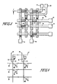
- the current path in the power bus 16 for current supplied to the right-hand gate G6 exceeds that for the left-hand gate G1 by five unit lengths, with a unit conductor length l in this case being equal to the distance between the connections of two adjacent gates to the power bus.
- the current path for current from the right-hand gate G6 is shorter than that for the left-hand gate G1 by the same five unit lengths. The same relationship holds true for all other pairs of gates.
- the total current path from the power bonding pad to the ground bonding pad is the same for all gates connected to the power and ground busses.
- the ground bus 16 is looped back on itself after the last connection in the direction of current flow.
- this return portion of the ground conductor is illustrated in Figure 9 as being located in the gates, it will be appreciated that it can overlay the connection portion of the ground bus in a separate layer, as illustrated with respect to Figure 8.
- the second design principle that is employed to control the voltage gradient relates to the cross-sectional area of the busses. More particularly, the cross-sectional area of each unit length is proportional to the amount of current carried by that unit length. Referring again to Figure 9, the width of each of the power and ground busses is stepped so that each conductor is widest where the magnitude of current is greatest and narrowest where the current is smallest. With this arrangement, the current density in each conductor is constant throughout the length of the conductor. Therefore, the voltage drop along each unit length of the conductors will be the same, so that the voltage gradient from gate to gate is uniform.
- each conductor will remain the same throughout the entirety of its length, due to the metallization process that is employed to deposit the metal layer on the substrate. Therefore, the control on the cross-sectional area of the conductor is obtained by regulating its width. In other words, the width of each unit length of the conductors is proportional to the current carried in that portion of the conductor.
- the variation in the width of each conductor is provided by means of discrete steps located along the length of the conductor.
- discrete step approach is preferred because it lends itself more readily to computer-aided design (CAD) of integrated circuit chips.
- CAD computer-aided design
- the changes in current magnitude within the conductor occur at discrete points, i.e. the points where the gates are connected, rather than continuously.
- the width changes of these two busses are complementary to one another. Consequently, it is possible to "nest" the two conductors with one another, achieving a savings in space on the surface of the chip. More particularly, the total width of the area occupied by the two busses along the portion of their lengths which is connected to the gates comprises the width of one of the busses at its widest point, the distance of the spacing between the conductors, and the width of the other conductor at its narrowest point. In contrast, two busses of constant width would occupy an area having a width equal to their total width plus the space between them.
- FIG. 9 illustrates that the current is conducted between each gate 12 and the busses 14 and 16 by means of a second set of conductors 50 and 52.
- the total length of the current path along these conductors should also be the same for each gate.
- the conductor 50 to the power bus 14 is connected to this bus along its edge that is closest to the gates, since that edge is the same distance from each gate.
- the conductor 52 to the ground bus 16 is connected to the edge of bus that is farthest from the gates, since this edge is also a constant distance from each gate.
- each pair of conductors 50 and 52 has the same length for all gates.
- the conductors 50 and 52 be connected to the edges of the busses, or that all conductors connected between one of the busses and the various gates have the same length. Rather, the criterion that is controlling is that the total current path from the power source to the ground reference be the same for each gate.
Applications Claiming Priority (2)
| Application Number | Priority Date | Filing Date | Title |
|---|---|---|---|
| US530636 | 1983-09-09 | ||
| US06/530,636 US4583111A (en) | 1983-09-09 | 1983-09-09 | Integrated circuit chip wiring arrangement providing reduced circuit inductance and controlled voltage gradients |
Related Parent Applications (1)
| Application Number | Title | Priority Date | Filing Date |
|---|---|---|---|
| EP84401771.5 Division | 1984-09-07 |
Publications (2)
| Publication Number | Publication Date |
|---|---|
| EP0306620A1 true EP0306620A1 (de) | 1989-03-15 |
| EP0306620B1 EP0306620B1 (de) | 1994-03-02 |
Family
ID=24114369
Family Applications (2)
| Application Number | Title | Priority Date | Filing Date |
|---|---|---|---|
| EP84401771A Expired EP0138650B1 (de) | 1983-09-09 | 1984-09-07 | Verdrahtungsanordnung für eine integrierte Schaltung mit verringerter Stromkreis-Induktion und bestimmten Spannungsabfällen |
| EP88108180A Expired - Lifetime EP0306620B1 (de) | 1983-09-09 | 1984-09-07 | Busstruktur für einen integrierten Schaltkreis |
Family Applications Before (1)
| Application Number | Title | Priority Date | Filing Date |
|---|---|---|---|
| EP84401771A Expired EP0138650B1 (de) | 1983-09-09 | 1984-09-07 | Verdrahtungsanordnung für eine integrierte Schaltung mit verringerter Stromkreis-Induktion und bestimmten Spannungsabfällen |
Country Status (5)
| Country | Link |
|---|---|
| US (1) | US4583111A (de) |
| EP (2) | EP0138650B1 (de) |
| JP (1) | JPS60143647A (de) |
| CA (1) | CA1223670A (de) |
| DE (2) | DE3486286T2 (de) |
Cited By (3)
| Publication number | Priority date | Publication date | Assignee | Title |
|---|---|---|---|---|
| EP0514615A1 (de) * | 1991-05-23 | 1992-11-25 | STMicroelectronics S.r.l. | Elektronische Leistungsanordnung realisiert durch eine Reihe elementarer Halbleiterbauelemente in Parallelverbindung und verwandtes Herstellungsverfahren |
| WO1993012540A1 (en) * | 1991-12-10 | 1993-06-24 | Vlsi Technology, Inc. | Integrated circuit with variable pad pitch |
| US11414657B2 (en) | 2015-06-29 | 2022-08-16 | Ionis Pharmaceuticals, Inc. | Modified CRISPR RNA and modified single CRISPR RNA and uses thereof |
Families Citing this family (28)
| Publication number | Priority date | Publication date | Assignee | Title |
|---|---|---|---|---|
| JPS6030152A (ja) * | 1983-07-28 | 1985-02-15 | Toshiba Corp | 集積回路 |
| US5202751A (en) * | 1984-03-30 | 1993-04-13 | Kabushiki Kaisha Toshiba | Semiconductor integrated circuit |
| US5165086A (en) * | 1985-02-20 | 1992-11-17 | Hitachi, Ltd. | Microprocessor chip using two-level metal lines technology |
| JPS61241964A (ja) * | 1985-04-19 | 1986-10-28 | Hitachi Ltd | 半導体装置 |
| JPS6230367U (de) * | 1985-08-07 | 1987-02-24 | ||
| JPH0815202B2 (ja) * | 1986-03-31 | 1996-02-14 | 株式会社東芝 | 半導体集積回路装置 |
| JPS6370550A (ja) * | 1986-09-12 | 1988-03-30 | Nec Corp | 半導体集積回路装置 |
| JPH01139437U (de) * | 1988-03-18 | 1989-09-22 | ||
| US5126822A (en) * | 1989-02-14 | 1992-06-30 | North American Philips Corporation | Supply pin rearrangement for an I.C. |
| US5006918A (en) * | 1989-07-24 | 1991-04-09 | International Business Machines Corporation | Floating orthogonal line structure for X-Y wiring planes |
| US5517015A (en) * | 1990-11-19 | 1996-05-14 | Dallas Semiconductor Corporation | Communication module |
| KR950012657B1 (en) * | 1991-01-22 | 1995-10-19 | Nec Co Ltd | Resin sealed semiconductor integrated circuit |
| JP3027990B2 (ja) * | 1991-03-18 | 2000-04-04 | 富士通株式会社 | 半導体装置の製造方法 |
| US5994770A (en) * | 1991-07-09 | 1999-11-30 | Dallas Semiconductor Corporation | Portable electronic data carrier |
| US5297099A (en) * | 1991-07-10 | 1994-03-22 | Dallas Semiconductor Corp. | Integrated circuit with both battery-powered and signal-line-powered areas |
| JP2825031B2 (ja) * | 1991-08-06 | 1998-11-18 | 日本電気株式会社 | 半導体メモリ装置 |
| US5289040A (en) * | 1991-08-12 | 1994-02-22 | National Semiconductor Corporation | Compensating lead structure for distributed IC components |
| JP3052519B2 (ja) * | 1992-01-14 | 2000-06-12 | 日本電気株式会社 | 集積回路の電源配線設計方法 |
| EP0713251B1 (de) * | 1992-11-18 | 1999-01-07 | Fuji Electric Co. Ltd. | Halbleiter-Umwandlungsvorrichtung |
| US5848541A (en) * | 1994-03-30 | 1998-12-15 | Dallas Semiconductor Corporation | Electrical/mechanical access control systems |
| US5831827A (en) * | 1994-04-28 | 1998-11-03 | Dallas Semiconductor Corporation | Token shaped module for housing an electronic circuit |
| US5604343A (en) * | 1994-05-24 | 1997-02-18 | Dallas Semiconductor Corporation | Secure storage of monetary equivalent data systems and processes |
| US5679944A (en) * | 1994-06-15 | 1997-10-21 | Dallas Semiconductor Corporation | Portable electronic module having EPROM memory, systems and processes |
| US5615130A (en) * | 1994-12-14 | 1997-03-25 | Dallas Semiconductor Corp. | Systems and methods to gather, store and transfer information from electro/mechanical tools and instruments |
| US6344667B1 (en) * | 1998-03-02 | 2002-02-05 | Kabushiki Kaisha Toshiba | Wiring board with reduced radiation of undesired electromagnetic waves |
| US6274896B1 (en) | 2000-01-14 | 2001-08-14 | Lexmark International, Inc. | Drive transistor with fold gate |
| US7035785B2 (en) * | 2001-12-28 | 2006-04-25 | Intel Corporation | Mechanism for estimating and controlling di/dt-induced power supply voltage variations |
| WO2006138564A1 (en) * | 2005-06-17 | 2006-12-28 | California Institute Of Technology | Analog bus driver and multiplexer |
Citations (1)
| Publication number | Priority date | Publication date | Assignee | Title |
|---|---|---|---|---|
| EP0074825A2 (de) * | 1981-09-10 | 1983-03-23 | Fujitsu Limited | Herstellung von integrierten Schaltungen nach dem Mutterscheibenverfahren |
Family Cites Families (10)
| Publication number | Priority date | Publication date | Assignee | Title |
|---|---|---|---|---|
| US3365707A (en) * | 1967-06-23 | 1968-01-23 | Rca Corp | Lsi array and standard cells |
| US3808475A (en) * | 1972-07-10 | 1974-04-30 | Amdahl Corp | Lsi chip construction and method |
| GB1487945A (en) * | 1974-11-20 | 1977-10-05 | Ibm | Semiconductor integrated circuit devices |
| JPS53140983A (en) * | 1977-05-16 | 1978-12-08 | Hitachi Ltd | Semiconductor integrated circuit |
| JPS60953B2 (ja) * | 1977-12-30 | 1985-01-11 | 富士通株式会社 | 半導体集積回路装置 |
| JPS5543840A (en) * | 1978-09-25 | 1980-03-27 | Hitachi Ltd | Power distributing structure of iil element |
| US4475119A (en) * | 1981-04-14 | 1984-10-02 | Fairchild Camera & Instrument Corporation | Integrated circuit power transmission array |
| JPS5858751A (ja) * | 1981-10-05 | 1983-04-07 | Hitachi Ltd | 集積回路装置 |
| JPS58124262A (ja) * | 1982-01-20 | 1983-07-23 | Nec Corp | 集積回路装置 |
| US4511914A (en) * | 1982-07-01 | 1985-04-16 | Motorola, Inc. | Power bus routing for providing noise isolation in gate arrays |
-
1983
- 1983-09-09 US US06/530,636 patent/US4583111A/en not_active Expired - Lifetime
-
1984
- 1984-09-07 DE DE3486286T patent/DE3486286T2/de not_active Expired - Fee Related
- 1984-09-07 EP EP84401771A patent/EP0138650B1/de not_active Expired
- 1984-09-07 CA CA000462640A patent/CA1223670A/en not_active Expired
- 1984-09-07 DE DE8484401771T patent/DE3478172D1/de not_active Expired
- 1984-09-07 EP EP88108180A patent/EP0306620B1/de not_active Expired - Lifetime
- 1984-09-10 JP JP59188256A patent/JPS60143647A/ja active Pending
Patent Citations (1)
| Publication number | Priority date | Publication date | Assignee | Title |
|---|---|---|---|---|
| EP0074825A2 (de) * | 1981-09-10 | 1983-03-23 | Fujitsu Limited | Herstellung von integrierten Schaltungen nach dem Mutterscheibenverfahren |
Non-Patent Citations (3)
| Title |
|---|
| IBM TECHNICAL DISCLOSURE BULLETIN, vol. 22, no. 5, October 1979, pages 2018-2020, New York, US; R.L. DONZE et al.: "Circuit layout technique for custom LSI components" * |
| PATENT ABSTRACTS OF JAPAN, vol. 3, no. 13 (E-88), 7th February 1979, page 95 E 88; & JP-A-53 140 983 (HITACHI SEISAKUSHO K.K.) 08-12-1978 * |
| PATENT ABSTRACTS OF JAPAN, vol. 6, no. 218 (E-139)[1096], 2nd November 1982; & JP-A-57 121 250 (TOKYO SHIBAURA DENKI K.K.) 28-07-1982 * |
Cited By (6)
| Publication number | Priority date | Publication date | Assignee | Title |
|---|---|---|---|---|
| EP0514615A1 (de) * | 1991-05-23 | 1992-11-25 | STMicroelectronics S.r.l. | Elektronische Leistungsanordnung realisiert durch eine Reihe elementarer Halbleiterbauelemente in Parallelverbindung und verwandtes Herstellungsverfahren |
| WO1993012540A1 (en) * | 1991-12-10 | 1993-06-24 | Vlsi Technology, Inc. | Integrated circuit with variable pad pitch |
| US5424248A (en) * | 1991-12-10 | 1995-06-13 | Vlsi Technology, Inc. | Method of making an integrated circuit with variable pad pitch |
| US5610417A (en) * | 1991-12-10 | 1997-03-11 | Vlsi Technology, Inc. | Integrated circuit with variable pad pitch |
| US5742079A (en) * | 1991-12-10 | 1998-04-21 | Vlsi Technology, Inc. | Integrated circuit with variable pad pitch |
| US11414657B2 (en) | 2015-06-29 | 2022-08-16 | Ionis Pharmaceuticals, Inc. | Modified CRISPR RNA and modified single CRISPR RNA and uses thereof |
Also Published As
| Publication number | Publication date |
|---|---|
| EP0138650B1 (de) | 1989-05-10 |
| EP0306620B1 (de) | 1994-03-02 |
| DE3486286D1 (de) | 1994-04-07 |
| DE3486286T2 (de) | 1994-09-29 |
| US4583111A (en) | 1986-04-15 |
| DE3478172D1 (en) | 1989-06-15 |
| EP0138650A1 (de) | 1985-04-24 |
| CA1223670A (en) | 1987-06-30 |
| JPS60143647A (ja) | 1985-07-29 |
Similar Documents
| Publication | Publication Date | Title |
|---|---|---|
| US4583111A (en) | Integrated circuit chip wiring arrangement providing reduced circuit inductance and controlled voltage gradients | |
| EP0374842B1 (de) | Integrierte Halbleiterschaltungsanordnung, die aus einem Sytem von Standardzellen besteht | |
| US4499484A (en) | Integrated circuit manufactured by master slice method | |
| US4207556A (en) | Programmable logic array arrangement | |
| JP4562908B2 (ja) | Asic配線アーキテクチャ | |
| US5119169A (en) | Semiconductor integrated circuit device | |
| US7155684B2 (en) | Integrated circuit device and method for forming the same | |
| US4811073A (en) | Gate array arrangement | |
| EP0360507B1 (de) | Integrierte Schaltungshalbleiteranordnung mit verbesserter Einrichtung für Speiseleitungen | |
| US5135889A (en) | Method for forming a shielding structure for decoupling signal traces in a semiconductor | |
| US5388055A (en) | Semiconductor integrated circuit having polycell structure and method of designing the same | |
| US5255156A (en) | Bonding pad interconnection on a multiple chip module having minimum channel width | |
| KR19980024593A (ko) | 반도체 집적회로, 그 설계방법 및 기록매체 | |
| EP0563973B1 (de) | Integrierte Masterslice-Schaltung mit reduzierten Chipabmessungen und vermindertem Speisespannungsrauschen | |
| US5223733A (en) | Semiconductor integrated circuit apparatus and method for designing the same | |
| KR20010102120A (ko) | 지그재그형 도전체 트랙을 갖는 집적 회로 및 이의 제조방법 | |
| US5270592A (en) | Clock supply circuit layout in a circuit area | |
| EP0103362A2 (de) | Halbleiteranordnungen mit Leistungslinien | |
| EP0782188A2 (de) | Gate-Array-Zellen-Architektur hoher Dichte | |
| EP0558133B1 (de) | Integrierte CMOS-Schaltung | |
| US6885043B2 (en) | ASIC routing architecture | |
| US4593205A (en) | Macrocell array having an on-chip clock generator | |
| US7392497B2 (en) | Regular routing for deep sub-micron chip design | |
| EP0098173A2 (de) | Integrierte Halbleiterschaltungsanordnung | |
| US7002253B2 (en) | Semiconductor device and design method thereof |
Legal Events
| Date | Code | Title | Description |
|---|---|---|---|
| PUAI | Public reference made under article 153(3) epc to a published international application that has entered the european phase |
Free format text: ORIGINAL CODE: 0009012 |
|
| AC | Divisional application: reference to earlier application |
Ref document number: 138650 Country of ref document: EP |
|
| AK | Designated contracting states |
Kind code of ref document: A1 Designated state(s): DE FR GB IT NL |
|
| 17P | Request for examination filed |
Effective date: 19890906 |
|
| 17Q | First examination report despatched |
Effective date: 19920414 |
|
| GRAA | (expected) grant |
Free format text: ORIGINAL CODE: 0009210 |
|
| AC | Divisional application: reference to earlier application |
Ref document number: 138650 Country of ref document: EP |
|
| AK | Designated contracting states |
Kind code of ref document: B1 Designated state(s): DE FR GB IT NL |
|
| REF | Corresponds to: |
Ref document number: 3486286 Country of ref document: DE Date of ref document: 19940407 |
|
| ET | Fr: translation filed | ||
| ITF | It: translation for a ep patent filed |
Owner name: STUDIO TORTA SOCIETA' SEMPLICE |
|
| PG25 | Lapsed in a contracting state [announced via postgrant information from national office to epo] |
Ref country code: GB Effective date: 19940907 |
|
| PLBE | No opposition filed within time limit |
Free format text: ORIGINAL CODE: 0009261 |
|
| STAA | Information on the status of an ep patent application or granted ep patent |
Free format text: STATUS: NO OPPOSITION FILED WITHIN TIME LIMIT |
|
| 26N | No opposition filed | ||
| PG25 | Lapsed in a contracting state [announced via postgrant information from national office to epo] |
Ref country code: NL Effective date: 19950401 |
|
| GBPC | Gb: european patent ceased through non-payment of renewal fee |
Effective date: 19940907 |
|
| NLV4 | Nl: lapsed or anulled due to non-payment of the annual fee | ||
| PG25 | Lapsed in a contracting state [announced via postgrant information from national office to epo] |
Ref country code: FR Effective date: 19950531 |
|
| PG25 | Lapsed in a contracting state [announced via postgrant information from national office to epo] |
Ref country code: DE Effective date: 19950601 |
|
| REG | Reference to a national code |
Ref country code: FR Ref legal event code: ST |