EP0301998B1 - Apparatus for adjusting initial position of melt surface - Google Patents
Apparatus for adjusting initial position of melt surface Download PDFInfo
- Publication number
- EP0301998B1 EP0301998B1 EP88710019A EP88710019A EP0301998B1 EP 0301998 B1 EP0301998 B1 EP 0301998B1 EP 88710019 A EP88710019 A EP 88710019A EP 88710019 A EP88710019 A EP 88710019A EP 0301998 B1 EP0301998 B1 EP 0301998B1
- Authority
- EP
- European Patent Office
- Prior art keywords
- melt
- seed crystal
- light
- initial position
- adjusting
- Prior art date
- Legal status (The legal status is an assumption and is not a legal conclusion. Google has not performed a legal analysis and makes no representation as to the accuracy of the status listed.)
- Expired - Lifetime
Links
- 239000013078 crystal Substances 0.000 claims description 54
- 239000000155 melt Substances 0.000 claims description 38
- 238000000034 method Methods 0.000 claims description 10
- 230000003287 optical effect Effects 0.000 claims description 2
- 230000001902 propagating effect Effects 0.000 claims 1
- XUIMIQQOPSSXEZ-UHFFFAOYSA-N Silicon Chemical compound [Si] XUIMIQQOPSSXEZ-UHFFFAOYSA-N 0.000 description 10
- 229910052710 silicon Inorganic materials 0.000 description 10
- 239000010703 silicon Substances 0.000 description 10
- 239000010453 quartz Substances 0.000 description 9
- VYPSYNLAJGMNEJ-UHFFFAOYSA-N silicon dioxide Inorganic materials O=[Si]=O VYPSYNLAJGMNEJ-UHFFFAOYSA-N 0.000 description 9
- 238000004519 manufacturing process Methods 0.000 description 4
- 238000005259 measurement Methods 0.000 description 4
- 230000002093 peripheral effect Effects 0.000 description 4
- OKTJSMMVPCPJKN-UHFFFAOYSA-N Carbon Chemical compound [C] OKTJSMMVPCPJKN-UHFFFAOYSA-N 0.000 description 3
- 229910002804 graphite Inorganic materials 0.000 description 3
- 239000010439 graphite Substances 0.000 description 3
- 239000000463 material Substances 0.000 description 2
- 239000000615 nonconductor Substances 0.000 description 2
- 235000012431 wafers Nutrition 0.000 description 2
- 238000005452 bending Methods 0.000 description 1
- 238000001514 detection method Methods 0.000 description 1
- 238000002474 experimental method Methods 0.000 description 1
- 230000005484 gravity Effects 0.000 description 1
Images
Classifications
-
- C—CHEMISTRY; METALLURGY
- C30—CRYSTAL GROWTH
- C30B—SINGLE-CRYSTAL GROWTH; UNIDIRECTIONAL SOLIDIFICATION OF EUTECTIC MATERIAL OR UNIDIRECTIONAL DEMIXING OF EUTECTOID MATERIAL; REFINING BY ZONE-MELTING OF MATERIAL; PRODUCTION OF A HOMOGENEOUS POLYCRYSTALLINE MATERIAL WITH DEFINED STRUCTURE; SINGLE CRYSTALS OR HOMOGENEOUS POLYCRYSTALLINE MATERIAL WITH DEFINED STRUCTURE; AFTER-TREATMENT OF SINGLE CRYSTALS OR A HOMOGENEOUS POLYCRYSTALLINE MATERIAL WITH DEFINED STRUCTURE; APPARATUS THEREFOR
- C30B15/00—Single-crystal growth by pulling from a melt, e.g. Czochralski method
- C30B15/20—Controlling or regulating
- C30B15/22—Stabilisation or shape controlling of the molten zone near the pulled crystal; Controlling the section of the crystal
- C30B15/26—Stabilisation or shape controlling of the molten zone near the pulled crystal; Controlling the section of the crystal using television detectors; using photo or X-ray detectors
-
- C—CHEMISTRY; METALLURGY
- C30—CRYSTAL GROWTH
- C30B—SINGLE-CRYSTAL GROWTH; UNIDIRECTIONAL SOLIDIFICATION OF EUTECTIC MATERIAL OR UNIDIRECTIONAL DEMIXING OF EUTECTOID MATERIAL; REFINING BY ZONE-MELTING OF MATERIAL; PRODUCTION OF A HOMOGENEOUS POLYCRYSTALLINE MATERIAL WITH DEFINED STRUCTURE; SINGLE CRYSTALS OR HOMOGENEOUS POLYCRYSTALLINE MATERIAL WITH DEFINED STRUCTURE; AFTER-TREATMENT OF SINGLE CRYSTALS OR A HOMOGENEOUS POLYCRYSTALLINE MATERIAL WITH DEFINED STRUCTURE; APPARATUS THEREFOR
- C30B15/00—Single-crystal growth by pulling from a melt, e.g. Czochralski method
- C30B15/20—Controlling or regulating
-
- Y—GENERAL TAGGING OF NEW TECHNOLOGICAL DEVELOPMENTS; GENERAL TAGGING OF CROSS-SECTIONAL TECHNOLOGIES SPANNING OVER SEVERAL SECTIONS OF THE IPC; TECHNICAL SUBJECTS COVERED BY FORMER USPC CROSS-REFERENCE ART COLLECTIONS [XRACs] AND DIGESTS
- Y10—TECHNICAL SUBJECTS COVERED BY FORMER USPC
- Y10T—TECHNICAL SUBJECTS COVERED BY FORMER US CLASSIFICATION
- Y10T117/00—Single-crystal, oriented-crystal, and epitaxy growth processes; non-coating apparatus therefor
- Y10T117/10—Apparatus
- Y10T117/1004—Apparatus with means for measuring, testing, or sensing
- Y10T117/1008—Apparatus with means for measuring, testing, or sensing with responsive control means
Definitions
- the present invention relates to an apparatus for adjusting the initial position of the surface of a melt, which is suitable for use in a monocrystal growing system employing the Czochralski method to adjust the vertical position of the surface of the melt before the growing of a monocrystal.
- a cylindrical bar of silicon monocrystal obtained by the Czochralski method is usually subjected to a grinding process before it is sliced into wafers for making of, for instance, integrated circuit devices.
- the outer peripheral surface of the silicon monocrystal bar is ground until the predetermined diameter is attained.
- a silicon monocrystal bar obtained by the Czochralski method has an increasingly large diameter (e.g., 158 mm) in recent years, and therefore the proportion of the volume of the material removed from the bar becomes inevitably larger than it was before even if the reduction in diameter is the same, resulting in an undesirable increase in production cost.
- the volume of the material removed from an unground bar of 600 mm in length and 158 mm in diameter is 298 cm3. Since there have been strong demands for lowered production costs particularly in recent years, it is considered to be very advantageous to enable a minimization of the reduction in diameter, particularly with respect to a monocrystal bar of the above-described type, which is expecially costly and precious.
- the reduction in diameter can be lessened by, for instance, improving the quick-response performance and the stability of control over the crystal diameter. It can also be lessened by improving the level of precision of a device used in the monocrystal growing system to measure the crystal diameter.
- the initial value of the depth of a melt within a quartz crucible has hitherto been calculated by measuring the weight of the silicon polycrystal before it is heated and melted, and by using the specific gravity of the melt.
- an apparatus for adjusting the initial position of the surface of a melt which is suitable for use in a monocrystal growing system employing the Czochralski method, comprising: electrical contact detecting means for detecting the electrical contact between a seed crystal and said melt; reference position detecting means disposed above said melt for detecting that the lower end of said seed crystal is at a reference position; pulse generating means for outputting a number of pulses proportional to the distance through which said seed crystal descends; and pulse counting means for counting the number of pulses generated while said seed crystal descends from said reference position to the position at which said seed crystal is brought into electrical contact with said melt, and for outoputting a vertical position of the surface of said melt and means for vertically moving said crucible on the basis of a value of the vertical position which has been measured before the growing of a crystal, in such manner that the distance between the surface of said melt and an image sensor for measuring the diameter of said crystal is maintained at a predetermined value.
- FIG. 1 to 4 illustrate embodiments of the present invention, wherein
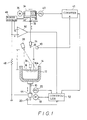
- Fig. 1 schematically shows the structure of a melt-surface initial position adjusting apparatus of the present invention.
- a quartz crucible 14 receiving a predetermined weight of polycrystal silicon is fitted in a graphite crucible 12 that is supported by the upper end of a crucible moving shaft 10.
- the polycrystal silicon is heated by a heater (not shown) surrounding the graphite crucible 12 so that it is melted to form a melt 16.
- the crucible moving shaft 10 is moved vertically by the operation of a motor 18 so that the upper surface of the melt 16 (i.e., a melt surface 16A) is adjusted to be positioned at a predetermined position.
- the vertical position of the crucible moving shaft 10 is detected by a lower-limit position detector 20 and by a pulse generator 22 which outputs a number of pulses proportional to the amount through which the crucible moving shaft 10 moves.
- the tip of a seed crystal 26 held by a seed crystal holder 24 is dipped into the melt 16 and then pulled up.
- the crystal diameter D at the boundary between the growing silicon monocrystal and the melt 16 is measured by processing a signal output by a TV camera 28 for industrial use.
- this embodiment provides an arrangement in which the distance H between the melt surface 16A and a reference position detector 30 disposed above the melt 16 is correctly measured, and, thereafter, the crucible moving shaft 10 is moved vertically in such a manner that the distance L is maintained at a predetermined value L0. This arrangement will be described below in detail.
- a wire rope 32 is wound on a drum 34 in such a manner as to be disposed in a helical groove formed in the peripheral surface of the drum 34, with one end of the rope 32 being secured to the drum 34. The other end of the rope 32 is secured to the upper end of the seed crystal holder 24.
- the drum 34 is rotatively driven by a motor 36 and is also driven axially via a screw rod (not shown) that is rotated by the motor 36. With this arrangement, the wire rope 32 unwound from the drum 34 is suspended without bending in the horizontal direction and extends downward passing through a guide 38. Accordingly, if the amount of rotation of the drum 34 is measured, the amount of vertical movement of the wire rope 32 can be correctly measured.
- the rotary shaft of the drum 34 is connected to the rotary shaft of a pulse generator 40 which outputs a number of pulses proportional to the amount of rotation of the drum 34 as well as signals indicative of the forward and backward rotation of the drum 34.
- Pulses and signals output from the pulse generator 40 are respectively supplied to the input terminal and the up/down control terminal of a counter 41.
- the counter 41 counts up or counts down the number of pulses supplied as the seed crystal 26 descends or ascends. The count of the counter 41 is cleared when the seed crystal 26 descends to a certain position at which its lower end is detected by the reference position detector 30.
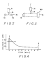
- Fig. 2 shows an example of the structure of the reference position detector 30.
- the seed crystal 26 is at the reference position when light radiated from a light emitter 60 is blocked by the tip of the descending seed crystal 26 and thus stops reaching a light receiver 62.
- the light emitter 60 and the light receiver 62 are disposed, for instance, on a shutter (not shown) above a chamber in which the crucibles 12 and 14 are disposed.
- the operation of the motor 36 is suspended, the shutter is opened, and the operation of the motor 36 is restarted, whereupon the seed crystal 26 descends further.
- the reference voltage V0 is determined by actually measuring, a plurality of times and under various conditions, values of the voltage V generated when the seed crystal 26 comes into contact with the melt 16, and it is set to a value at which V > V0 is always satisfied at the time of the contact.
- Fig. 4 shows the results obtained by measuring change with time in the voltage V across the terminals of the resistor 48, using, as the power source 46, a DC power source having an output voltage of 12V.
- A denotes the time at which the seed crystal 26 is dipped into the melt 16
- B denotes the time at which the tail of a grown crystal bar is separated from the melt 16.
- a quartz crucible such as the crucible 14, has conventionally been believed to be an electrical insulator.
- the present inventors have found from experiments that a quartz crucible exhibits electrical conductivity when it is at high temperatures above 1000°C.
- a signal output from the comparator 50 is supplied to a controller 52.
- the controller 52 operates to rotate the motor 36 in the reverse direction so as to slightly wind up the wire rope 32, thereby separating the seed crystal 26 from the melt 16.
- the controller 52 operates to read the count supplied from the counter 41 and compare the read count with a set value stored in the controller 52. Based on the result of this comparison, the controller 52 starts the motor 18, while counting up the pulses output from the pulse generator 22. In this way, the crucible moving shaft 10 is vertically moved so that the distance L between the TV camera 28 and the melt surface 16A becomes equal to the predetermined value L0.
- the location at which the reference position detector 30 is provided cannot be freely chosen due to limitations set by factors such as the structure of the crystal bar puller, it is preferred that the detector 30 be located as close as possible to the melt surface 16A. For instance, if the distance between the drum 34 and the melt surface 16A is about 3 m and the distances H and L are each about 1 m, the provision of the detector 30 at such a preferable location makes it possible to measure the distance H with a small error that is about one third of what is possible where the detector 30 is disposed in the vicinity of the guide 38.
- the crucible moving shaft 10 is moved vertically in such a manner that the melt surface 16A is always positioned at a predetermined position.
- the vertical position of the melt surface 16A during the operation of growing a monocrystal is calculated from a reduction rate of the melt 16 that is calculated by integrating with respect to time the product of the cross-sectional area of the growing monocrystal and the speed at which the seed crystal 26 is pulled up from the melt surface 16A, as well as from the rate at which the wire rope 32 is wound up and the rate at which the crucible moving shaft 10 is moved upward.
- the distance L between the melt surface 16A and the camera 28 is calculated on the basis of the thus calculated position of the melt surface 16A.
- the crystal diameter D was measured by processing signals output from the industrial-use TV camera 28 according to the above formula, the measurement deviation was reduced by about 0.3 mm from the deviation conventionally involved. Since various other factors cause increases in the measurement deviation, if suitable measures are taken to prevent increases by individual factors, it is possible to reduce the measurement deviation by a total reduction on the order of 1 mm.
- FIG. 3 A second embodiment of the present invention will now be described with reference to Fig. 3.
- An apparatus in accordance with this embodiment has the same structure as that of the previous embodiment, except for the provision of a different reference position detector 30A.
- the reference position detector 30A has a light emitter/receiver 64 and a right-angle prism 66 which are disposed on either side of the path along which the seed crystal 26 descends.
- wire rope 32 is used, a shaft may be used instead of the wire rope 32.
- an AC power source may be used instead of the DC power source 46.
- the industrial-use TV camera 28 used as an image sensor for measuring the crystal diameter has a pickup tube
- a solid-state image sensor such as a CCD may alternatively be used.
- the apparatus of the present invention is applied to a silicon monocrystal growing system, the present invention is not limited thereto.
- the apparatus of the present invention is applicable to systems for growing monocrystals of various types, insofar as the system employs the Czochralski method.
- the apparatus in accordance with the present invention ensures that the crystal-diameter measuring device measures the relevant dimension with an enhanced level of precision.
- This feature of the apparatus enables the outer peripheral surface of the resultant crystal bar to be ground by a lesser reduction in diameter during a grinding process before a process of slicing the bar into wafers, thus enabling a reduction in production costs.
Landscapes
- Chemical & Material Sciences (AREA)
- Engineering & Computer Science (AREA)
- Crystallography & Structural Chemistry (AREA)
- Materials Engineering (AREA)
- Metallurgy (AREA)
- Organic Chemistry (AREA)
- Crystals, And After-Treatments Of Crystals (AREA)
Applications Claiming Priority (2)
| Application Number | Priority Date | Filing Date | Title |
|---|---|---|---|
| JP62181722A JPS6424089A (en) | 1987-07-21 | 1987-07-21 | Device for adjusting initial position of melt surface |
| JP181722/87 | 1987-07-21 |
Publications (2)
| Publication Number | Publication Date |
|---|---|
| EP0301998A1 EP0301998A1 (en) | 1989-02-01 |
| EP0301998B1 true EP0301998B1 (en) | 1992-09-30 |
Family
ID=16105731
Family Applications (1)
| Application Number | Title | Priority Date | Filing Date |
|---|---|---|---|
| EP88710019A Expired - Lifetime EP0301998B1 (en) | 1987-07-21 | 1988-07-21 | Apparatus for adjusting initial position of melt surface |
Country Status (4)
| Country | Link |
|---|---|
| US (1) | US4915775A (enExample) |
| EP (1) | EP0301998B1 (enExample) |
| JP (1) | JPS6424089A (enExample) |
| DE (1) | DE3875015T2 (enExample) |
Families Citing this family (26)
| Publication number | Priority date | Publication date | Assignee | Title |
|---|---|---|---|---|
| JPH0776144B2 (ja) * | 1988-11-21 | 1995-08-16 | 信越半導体株式会社 | 結晶引上ワイヤの偏芯量測定装置 |
| JP2678383B2 (ja) * | 1989-05-30 | 1997-11-17 | 信越半導体 株式会社 | 単結晶上装置 |
| JPH0726817B2 (ja) * | 1990-07-28 | 1995-03-29 | 信越半導体株式会社 | 結晶径測定装置 |
| JPH0785489B2 (ja) * | 1991-02-08 | 1995-09-13 | 信越半導体株式会社 | 単結晶の直径計測方法 |
| WO1992019797A1 (fr) * | 1991-04-26 | 1992-11-12 | Mitsubishi Materials Corporation | Procede de tirage de cristal unique |
| DE4123336A1 (de) * | 1991-07-15 | 1993-01-21 | Leybold Ag | Kristallziehverfahren und vorrichtung zu seiner durchfuehrung |
| US5286461A (en) * | 1991-09-20 | 1994-02-15 | Ferrofluidics Corporation | Method and apparatus for melt level detection in czochralski crystal growth systems |
| DE4231162C2 (de) * | 1992-09-17 | 1996-03-14 | Wacker Siltronic Halbleitermat | Verfahren zur Regelung der Schmelzenhöhe während des Ziehens von Einkristallen |
| JP2823035B2 (ja) * | 1993-02-10 | 1998-11-11 | 信越半導体株式会社 | 半導体単結晶の引上装置及び引上方法 |
| US5582642A (en) * | 1995-06-20 | 1996-12-10 | Memc Electronic Materials, Inc. | Apparatus and method for adjusting the position of a pull wire of a crystal pulling machine |
| US5888299A (en) * | 1995-12-27 | 1999-03-30 | Shin-Etsu Handotai Co., Ltd. | Apparatus for adjusting initial position of melt surface |
| US6071340A (en) * | 1996-02-28 | 2000-06-06 | General Signal Technology Corporation | Apparatus for melt-level detection in Czochralski crystal growth systems |
| JP3758743B2 (ja) * | 1996-04-22 | 2006-03-22 | コマツ電子金属株式会社 | 半導体単結晶製造装置 |
| DE19652543A1 (de) * | 1996-12-17 | 1998-06-18 | Wacker Siltronic Halbleitermat | Verfahren zur Herstellung eines Silicium-Einkristalls und Heizvorrichtung zur Durchführung des Verfahrens |
| US5961716A (en) * | 1997-12-15 | 1999-10-05 | Seh America, Inc. | Diameter and melt measurement method used in automatically controlled crystal growth |
| US6030451A (en) * | 1998-01-12 | 2000-02-29 | Seh America, Inc. | Two camera diameter control system with diameter tracking for silicon ingot growth |
| US6106612A (en) * | 1998-06-04 | 2000-08-22 | Seh America Inc. | Level detector and method for detecting a surface level of a material in a container |
| JP4561513B2 (ja) | 2005-07-22 | 2010-10-13 | 株式会社Sumco | 単結晶引き上げ装置の液面位置調整機構及び液面位置調整方法並びに単結晶引き上げ装置の液面位置合わせ機構及び液面位置合わせ方法 |
| JP5678635B2 (ja) | 2010-12-13 | 2015-03-04 | 株式会社Sumco | シリコン単結晶の製造装置、シリコン単結晶の製造方法 |
| JP5664573B2 (ja) | 2012-02-21 | 2015-02-04 | 信越半導体株式会社 | シリコン融液面の高さ位置の算出方法およびシリコン単結晶の引上げ方法ならびにシリコン単結晶引上げ装置 |
| JP6078974B2 (ja) | 2012-04-04 | 2017-02-15 | 株式会社Sumco | シリコン単結晶の製造方法 |
| DE112015003765B4 (de) | 2014-09-12 | 2022-02-03 | Shin-Etsu Handotai Co., Ltd. | Verfahren zum Herstellen eines Einkristalls |
| JP6536345B2 (ja) | 2015-10-14 | 2019-07-03 | 信越半導体株式会社 | 単結晶製造装置及び融液面位置の制御方法 |
| JP6390579B2 (ja) | 2015-10-19 | 2018-09-19 | 信越半導体株式会社 | 単結晶の製造方法 |
| AT526111B1 (de) | 2022-05-05 | 2024-04-15 | Fametec Gmbh | Vorrichtung und Verfahren zur Herstellung eines künstlichen Saphir-Einkristalls |
| CN117166043A (zh) * | 2023-09-21 | 2023-12-05 | 中环领先半导体材料有限公司 | 一种控制直拉单晶液面距的方法 |
Family Cites Families (8)
| Publication number | Priority date | Publication date | Assignee | Title |
|---|---|---|---|---|
| US3998598A (en) * | 1973-11-23 | 1976-12-21 | Semimetals, Inc. | Automatic diameter control for crystal growing facilities |
| US4207293A (en) * | 1974-06-14 | 1980-06-10 | Varian Associates, Inc. | Circumferential error signal apparatus for crystal rod pulling |
| US3980438A (en) * | 1975-08-28 | 1976-09-14 | Arthur D. Little, Inc. | Apparatus for forming semiconductor crystals of essentially uniform diameter |
| DE3049376A1 (de) * | 1980-12-29 | 1982-07-29 | Heliotronic Forschungs- und Entwicklungsgesellschaft für Solarzellen-Grundstoffe mbH, 8263 Burghausen | Verfahren zur herstellung vertikaler pn-uebergaenge beim ziehen von siliciumscheiben aus einer siliciumschmelze |
| JPS5933554B2 (ja) * | 1982-08-19 | 1984-08-16 | 株式会社東芝 | 結晶成長装置 |
| JPS6021893A (ja) * | 1983-07-12 | 1985-02-04 | Toshiba Corp | 単結晶の製造装置 |
| JPS6186493A (ja) * | 1984-10-04 | 1986-05-01 | Toshiba Mach Co Ltd | 半導体結晶引上機 |
| JPH0649631B2 (ja) * | 1986-10-29 | 1994-06-29 | 信越半導体株式会社 | 結晶径測定装置 |
-
1987
- 1987-07-21 JP JP62181722A patent/JPS6424089A/ja active Granted
-
1988
- 1988-07-21 DE DE8888710019T patent/DE3875015T2/de not_active Expired - Fee Related
- 1988-07-21 US US07/222,438 patent/US4915775A/en not_active Expired - Lifetime
- 1988-07-21 EP EP88710019A patent/EP0301998B1/en not_active Expired - Lifetime
Also Published As
| Publication number | Publication date |
|---|---|
| DE3875015T2 (de) | 1993-03-04 |
| JPS6424089A (en) | 1989-01-26 |
| EP0301998A1 (en) | 1989-02-01 |
| JPH0559876B2 (enExample) | 1993-09-01 |
| DE3875015D1 (de) | 1992-11-05 |
| US4915775A (en) | 1990-04-10 |
Similar Documents
| Publication | Publication Date | Title |
|---|---|---|
| EP0301998B1 (en) | Apparatus for adjusting initial position of melt surface | |
| EP0315572B1 (en) | Apparatus for measuring the diameter of a crystal | |
| EP0265805B1 (en) | Apparatus for measuring crystal diameter | |
| KR101028684B1 (ko) | 실리콘 단결정 인상 방법 | |
| US6241818B1 (en) | Method and system of controlling taper growth in a semiconductor crystal growth process | |
| US5725660A (en) | Semiconductor single crystal growing apparatus | |
| US6030451A (en) | Two camera diameter control system with diameter tracking for silicon ingot growth | |
| JP3606037B2 (ja) | 単結晶引上げ装置の原料追加供給装置 | |
| EP0425837B1 (en) | Method of adjusting concentration of oxygen in silicon single crystal and apparatus for use in the method | |
| JP5404264B2 (ja) | 単結晶シリコンの製造方法及び単結晶シリコンの製造装置 | |
| JP4360163B2 (ja) | 単結晶の製造装置及び単結晶の製造方法 | |
| JP4325389B2 (ja) | 融液面初期位置調整装置及び融液面初期位置調整方法並びに単結晶の製造方法 | |
| JP4277681B2 (ja) | 単結晶引上げ装置の融液表面位置検出装置及びその単結晶引上げ装置 | |
| JP2019214486A (ja) | 融液面と種結晶の間隔測定方法、種結晶の予熱方法、及び単結晶の製造方法 | |
| EP0781872A2 (en) | Apparatus and method for adjusting initial position of melt surface | |
| EP0288605B1 (en) | Method of and apparatus for controlling floating zone of semiconductor rod | |
| JP2840213B2 (ja) | 単結晶の直径測定方法および直径測定装置 | |
| JPH07277879A (ja) | Cz法による単結晶製造装置および融液レベル制御方法 | |
| US3259467A (en) | Apparatus for pulling rod-shaped crystals of semiconductor material from a melt in acrucible | |
| JPH0331674B2 (enExample) | ||
| KR102147462B1 (ko) | 단결정 잉곳 성장 장치 | |
| JP6090501B2 (ja) | 単結晶引き上げ方法 | |
| KR101366725B1 (ko) | 멜트갭 제어 시스템 및 이를 포함한 실리콘 단결정 성장 장치 | |
| JPH03137091A (ja) | 半導体単結晶の製造方法 | |
| CN121729529A (zh) | 硅原料的高度的变化量的测量方法及使用其的单晶硅的制造方法及单晶硅制造装置 |
Legal Events
| Date | Code | Title | Description |
|---|---|---|---|
| PUAI | Public reference made under article 153(3) epc to a published international application that has entered the european phase |
Free format text: ORIGINAL CODE: 0009012 |
|
| AK | Designated contracting states |
Kind code of ref document: A1 Designated state(s): DE FR GB |
|
| 17P | Request for examination filed |
Effective date: 19890707 |
|
| 17Q | First examination report despatched |
Effective date: 19910412 |
|
| GRAA | (expected) grant |
Free format text: ORIGINAL CODE: 0009210 |
|
| AK | Designated contracting states |
Kind code of ref document: B1 Designated state(s): DE FR GB |
|
| ET | Fr: translation filed | ||
| REF | Corresponds to: |
Ref document number: 3875015 Country of ref document: DE Date of ref document: 19921105 |
|
| PLBE | No opposition filed within time limit |
Free format text: ORIGINAL CODE: 0009261 |
|
| STAA | Information on the status of an ep patent application or granted ep patent |
Free format text: STATUS: NO OPPOSITION FILED WITHIN TIME LIMIT |
|
| 26N | No opposition filed | ||
| PGFP | Annual fee paid to national office [announced via postgrant information from national office to epo] |
Ref country code: FR Payment date: 19990709 Year of fee payment: 12 |
|
| PGFP | Annual fee paid to national office [announced via postgrant information from national office to epo] |
Ref country code: GB Payment date: 19990721 Year of fee payment: 12 |
|
| PG25 | Lapsed in a contracting state [announced via postgrant information from national office to epo] |
Ref country code: GB Free format text: LAPSE BECAUSE OF NON-PAYMENT OF DUE FEES Effective date: 20000721 |
|
| GBPC | Gb: european patent ceased through non-payment of renewal fee |
Effective date: 20000721 |
|
| PG25 | Lapsed in a contracting state [announced via postgrant information from national office to epo] |
Ref country code: FR Free format text: LAPSE BECAUSE OF NON-PAYMENT OF DUE FEES Effective date: 20010330 |
|
| REG | Reference to a national code |
Ref country code: FR Ref legal event code: ST |
|
| PGFP | Annual fee paid to national office [announced via postgrant information from national office to epo] |
Ref country code: DE Payment date: 20010716 Year of fee payment: 14 |
|
| PG25 | Lapsed in a contracting state [announced via postgrant information from national office to epo] |
Ref country code: DE Free format text: LAPSE BECAUSE OF NON-PAYMENT OF DUE FEES Effective date: 20030201 |