EP0293575A2 - Circuit intégré comportant un dispositif de protection - Google Patents
Circuit intégré comportant un dispositif de protection Download PDFInfo
- Publication number
- EP0293575A2 EP0293575A2 EP88105515A EP88105515A EP0293575A2 EP 0293575 A2 EP0293575 A2 EP 0293575A2 EP 88105515 A EP88105515 A EP 88105515A EP 88105515 A EP88105515 A EP 88105515A EP 0293575 A2 EP0293575 A2 EP 0293575A2
- Authority
- EP
- European Patent Office
- Prior art keywords
- semiconductor
- integrated circuit
- resistance
- circuit arrangement
- zone
- Prior art date
- Legal status (The legal status is an assumption and is not a legal conclusion. Google has not performed a legal analysis and makes no representation as to the accuracy of the status listed.)
- Granted
Links
Images


Classifications
-
- H—ELECTRICITY
- H10—SEMICONDUCTOR DEVICES; ELECTRIC SOLID-STATE DEVICES NOT OTHERWISE PROVIDED FOR
- H10D—INORGANIC ELECTRIC SEMICONDUCTOR DEVICES
- H10D89/00—Aspects of integrated devices not covered by groups H10D84/00 - H10D88/00
- H10D89/60—Integrated devices comprising arrangements for electrical or thermal protection, e.g. protection circuits against electrostatic discharge [ESD]
-
- H—ELECTRICITY
- H10—SEMICONDUCTOR DEVICES; ELECTRIC SOLID-STATE DEVICES NOT OTHERWISE PROVIDED FOR
- H10D—INORGANIC ELECTRIC SEMICONDUCTOR DEVICES
- H10D1/00—Resistors, capacitors or inductors
- H10D1/40—Resistors
- H10D1/43—Resistors having PN junctions
-
- H—ELECTRICITY
- H10—SEMICONDUCTOR DEVICES; ELECTRIC SOLID-STATE DEVICES NOT OTHERWISE PROVIDED FOR
- H10D—INORGANIC ELECTRIC SEMICONDUCTOR DEVICES
- H10D84/00—Integrated devices formed in or on semiconductor substrates that comprise only semiconducting layers, e.g. on Si wafers or on GaAs-on-Si wafers
- H10D84/40—Integrated devices formed in or on semiconductor substrates that comprise only semiconducting layers, e.g. on Si wafers or on GaAs-on-Si wafers characterised by the integration of at least one component covered by groups H10D12/00 or H10D30/00 with at least one component covered by groups H10D10/00 or H10D18/00, e.g. integration of IGFETs with BJTs
- H10D84/401—Combinations of FETs or IGBTs with BJTs
- H10D84/403—Combinations of FETs or IGBTs with BJTs and with one or more of diodes, resistors or capacitors
Definitions
- the invention relates to a circuit arrangement with an at least partially integrated protective arrangement which protects the integrated circuit arrangement from high-energy electrical disturbances which act on it.
- Energy-rich electrical disturbances are, for example, disturbances which arise from electrostatic discharges and which can affect their connections when handling integrated circuits and can thereby cause irreversible changes in the integrated circuit until they are destroyed.
- electrostatic discharges occur in various types and strengths and are therefore difficult to describe in detail.
- integrated circuits are increasingly subjected to stress tests, in which electronic components are simulated by means of certain test arrangements, as is generally the case with electronic components. In these tests, the connections of the integrated circuit are subjected to a specific pulse load according to a prescribed scheme.
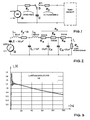
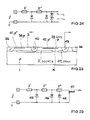
- FIG. 1 shows the first version of a test circuit.
- the capacitor C is charged by a voltage source Q via the resistor R1 and discharged by switching the switch S via the resistor R2 and the test object.
- Resistor R2 only serves to protect source Q and to avoid dangerous body currents in the event of contact.
- the second version of a test circuit is shown in FIG. 4.
- the test circuit of FIG. 4 differs from the test circuit of FIG. 1 in that the resistor R2 of the first version is omitted. By eliminating the resistor R2 in the second version, the full electrical energy of the charged capacitor C acts on the test object in the test circuit of the second version (FIG. 4).
- the first version of the test circuit is primarily used for testing MOS circuits, while the second version is increasingly being used for testing bipolar integrated circuits.
- the corresponding test regulations state that the tests must be carried out with both polarities.
- test methods carried out on integrated circuits have shown that the appearance of the damaged components is that which occurs in practice Appearance largely corresponds, so that the test methods described are used more and more for the assessment of integrated circuits.
- Such test methods for evaluating the protective arrangement are also used to develop protective arrangements for integrated circuits.
- FIG. 2 shows the equivalent circuit used for the simulation of the test circuit according to FIG. 1 (version 1).
- the test object was initially replaced by an ohmic load resistance R L.
- the load resistance R L was initially set at 1 ohm.
- the switching process of the switch S is simulated by a voltage jump in the generator Q.
- the decisive switching elements of the discharge circuit are represented in FIG. 2 by the switching elements C, L1, R3, C1, L2, R4, C2, R5, C3, R6 and R L.
- the inductance L1 of the equivalent circuit according to FIG. 2 characterizes the connection inductance of the capacitor C.
- the resistor R3 characterizes the contact resistances of the switch S and the capacitor C1 represents the capacitance of the switch S in the switch position K1 and the supply capacitance to resistor R2.
- Resistor R2 is simulated by switching elements L2, R4, R5, C3 and R6.
- the load is simulated by the resistor R L.
- FIG. 3 shows the result of the simulation on the basis of the equivalent circuit according to FIG. 2.
- the voltage generator Q was switched from zero to 2000 V (plus).
- the current shown in Figure 3 is the current that flows through the load resistor.
- FIG. 5 shows the equivalent circuit for the test circuit according to FIG. 4.
- the inductance L3 characterizes the self-inductance of the discharge circuit, while the resistor R7 characterizes the self-damping of the discharge circuit.
- the load is simulated by R L.
- FIG. 6 shows the result of the simulation with the aid of the equivalent circuit according to FIG. 5, namely for a voltage jump of the generator Q at zero time from zero to 500 V.
- R L also has a value of 1 ohm.
- the simulated time range extends from 0 to 100 nsec.
- the power-time profile of FIG. 7 has also been obtained by simulation, namely by product formation of voltage and current at the resistor R L.
- the diagrams show that the short-term load is significantly higher the higher the load resistance in the range of values shown.
- the invention is based on the object of specifying a protective arrangement for an integrated circuit arrangement which protects itself from the aforementioned undesirable disturbances which act on the integrated circuit and greatly reduces or reduces the influence of the disturbance on the downstream integrated circuit arrangement to be protected Protection brings about.
- This object is achieved in an integrated circuit arrangement of the type mentioned according to the invention solved that the protective arrangement has an ohmic resistance in the form of one or more resistance areas, which is designed such that it absorbs the essential part of the energy of the electrical disturbance at the limit load and that it absorbs the heat generated by the energy absorption in it, distributed over such an area of the protective circuit that the area of the protective arrangement covered by the thermal energy of the ohmic resistance is not thermally overloaded, and that the protective arrangement for limiting the interference voltage has one voltage-limiting element or several voltage-limiting elements.
- the voltage-limiting element or the voltage-limiting elements is (are) preferably designed such that the discharge energy supplied to them (them) does not overload the voltage-limiting element or the voltage-limiting elements.
- the ohmic resistance areas can be designed, for example, as resistance zones in the semiconductor body and / or as a metal conductor track on the surface of the integrated circuit arrangement.
- a resistor in the semiconductor region is preferably arranged at a distance from the semiconductor surface in accordance with a buried layer.
- Resistance zones in the semiconductor body can also be found in the surface Chen range be arranged, for example by an n+ zone, which is formed by a collector connection diffusion into a high-resistance, low-doped n-area (epitaxial layer).
- n+ zone which is formed by a collector connection diffusion into a high-resistance, low-doped n-area (epitaxial layer).
- p+ diffusion which is introduced into a buried layer zone through an n-epitaxial layer.
- Another aspect for the formation of the resistance zone according to the invention is the avoidance of a field strength breakthrough in the resistance zone.
- the resistance zone can become ineffective or partially ineffective through a field strength breakthrough. This can e.g. result from the fact that the breakthrough section bridges the resistance zone in whole or in part.
- the resistance zone must therefore be designed so that the breakdown field strength (2 ... 10 x 105 V / cm) cannot occur at any point in the resistance zone when the maximum stress load occurs.
- the discharge energy is partially converted into thermal energy in the substrate of the semiconductor body (substrate for protective arrangement and integrated circuit arrangement) by conducting the discharge process over the substrate region serving as a resistor.
- This has the advantage that the remaining parts of the protective arrangement can be dimensioned smaller in terms of the crystal area requirement, since their electrical load is lower.
- Another advantage of using the substrate resistance is that the voltage drop in the substrate area is not a voltage load for the zone between the connection pad and the underlying substrate area is effective when this substrate area is connected to the substrate area of the protective arrangement. If the substrate resistance is used, however, it should be noted that, due to the voltage drop in the decisive substrate resistance, the output potential of the protective arrangement is reduced or increased by the voltage drop across the substrate resistance when the fault occurs, depending on the polarity of the fault.
- the substrate region of the protective arrangement from the other substrate regions of the integrated circuit and to connect the substrate region of the protective arrangement to the reference point (ground) of the integrated circuit via a separate interconnect, the desired (required) substrate resistance of the protective arrangement appropriate formation of the separation connection zone can be realized.
- a "decoupling" of the substrate area of the protective arrangement from the substrate areas of the rest Integrated circuit has the advantage that, in the event of a fault, a greater protective effect for other integrated circuit parts is achieved, going beyond the directly protected circuit part.
- a "decoupling" of the substrate region of the protective arrangement from the substrate regions of the other circuit parts can be realized, for example, by enclosing a zone with relatively low conductivity around the substrate region of the associated connection pad of the integrated circuit, which zone covers the low-resistance substrate region of the protective arrangement from separates the other low-resistance substrate areas of the integrated circuit.
- the low-resistance substrate regions are generally formed by a p-type separation diffusion, while the relatively low conductivity zone is determined by the low-doped p-type region of the substrate material of the semiconductor body.
- FIGS. 10 to 14 show the manufacture of a protective arrangement according to the invention, which is intended to protect an integrated circuit arrangement which is located in the same semiconductor body as the protective arrangement, but is not shown in the following figures.
- the manufacture of the protective arrangement starts with a semiconductor body 1 (also semiconductor bodies of the integrated scarf, not shown) line arrangement), which in the exemplary embodiment has the p-line type.
- a resistance region 2 is introduced into the semiconductor body 1, the conductivity type of which is opposite to that of the semiconductor body 1 and which therefore has the n-conductivity type in FIG.
- the resistance region 2 is relatively heavily doped and has, for example, an impurity concentration of 1019 cm3.
- an epitaxial layer 3 of the n-type is applied to the semiconductor body 1 (substrate) of the p-type with the resistance region 2 of the n-type, so that the resistance region 2 between the substrate 1 and the epitaxial layer 3 is buried (buried layer).
- a semiconductor zone 4 of the p-conductivity type is introduced into the epitaxial layer 3, the regions 4 ', 4 ⁇ and 4 ′′′ of which form a zener diode with the adjacent resistance region 2, which serves as a voltage-limiting element.
- the p-regions 4 'and 4 ⁇ additionally perform the function of a separation zone together with the p-region 4 ⁇ ⁇ .
- the p-area 4 ′′′ touches the resistance area 2 on the entire underside, while the p-area 4 'touches the resistance area only at the edge.
- the p-regions 4 ', 4 ⁇ , 4 ′′′ and 4 ⁇ ⁇ are introduced so deep that they touch the resistance region 2 or the substrate 1.
- the p-zone 4 is introduced into the semiconductor body consisting of substrate 1 and epitaxial layer 3 in one operation, for example by diffusion or by ion implantation.
- connection of the resistance area 2 takes place according to the figure 13 through the connection zones 5 and 6 of the n-type, which are produced after the p-areas, for example also by diffusion or by ion implantation.
- the connection zone 5 of FIG. 13 serves to supply current for the resistance area 2 and lies in the middle of the resistance area 2.
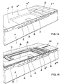
- FIG. 14 shows the finished protective arrangement with an insulating layer 7 on the surface of the epitaxial layer 3 and with an interconnect 8, which leads to the connection zone 5, with an interconnect 9, which connects the p-regions 4 ', 4 ⁇ and 4 ′′′ to one another and with an interconnect 10, which establishes an electrical connection between the connection zone 6 and the subsequent integrated circuit arrangement, not shown, in the same semiconductor body.
- FIG. 15 shows the top view of the protective arrangement of FIG. 14.
- a conductive path 9 ' is specified, the reference point of the subsequent integrated circuit, not shown, to be protected with the reference point (p-areas 4, 4', 4 ⁇ , 4 '' ') of the voltage-limiting Zener diode according to the arrangement according to the invention of Figure 13 connects.
- Figure 16 shows the equivalent circuit diagram of the protective arrangement of Figures 14 and 15.
- the resistance area 2 is divided into the resistance areas 2 ', 2 ⁇ and 2''' because in the embodiment of the invention according to Figures 14 and 15 a large-area diode becomes effective between the resistance region 2 and the substrate 1, which is formed by the pn junction between the resistance region 2 and the substrate 1.
- this diode is represented in a simplified manner by diodes 11 and 12.
- the Zener diode is designated by the reference number 13.
- the resistor 14 shown in broken lines represents the substrate resistance.
- the connection points of the circuit are designated by the reference numerals 15 and 16.
- the mode of operation of the protective arrangement can be explained with the aid of the equivalent circuit according to FIG. 16. If one of the described disturbances occurs at the connection terminals 15 and 16, then with positive polarity of the interference voltage occurring between connection 15 and 16 the current through the resistors 2 ', 2 ⁇ , 2''', the Zener diode 13 as a voltage-limiting element, and the substrate resistor 14 flow. The diodes 11 and 12 are then blocked. If the interference voltage between 15 and 16 has a negative polarity, the diodes 11 and 12 become conductive, that is to say that the current caused by the interference via the resistance regions 2 ', 2 ⁇ and 2''' to the substrate via the then effective in the direction of flow Diodes 11, 12 and 13 flows off.
- the resistance areas 2 ', 2 ⁇ , 2''' and 14 are dimensioned and designed so that they absorb the major part of the energy at the expected peak load up to which the protective arrangement has to perform its function and which generates heat to a larger crystal volume.
- the connection point from the anode of the Zener diode 13 and the substrate region of the Zener diode 13 is selected as the reference point for the subsequent circuit.
- FIG. 17 in order to produce this protective arrangement in a semiconductor body consisting of a substrate 1 of the p-type conduction, a buried layer 2 (resistance region) of the n-conduction type and an epitaxial layer 3 of the n-conduction type, the p-zones 15 , 16 and 17 of the n-conductivity type are introduced, namely until they come into contact with the substrate 1.
- the p-zones 15, 16 and 17 are produced, for example, by diffusion or by ion implantation.
- the p-zone 15 serves as a separation zone, while the p-zones 16 and 17 are semiconductor zones of Zener diodes.
- connection zones 18, 19 and 20 for the resistance region 2 are produced according to FIG.
- the connection zones 18, 19 and 20 have the n-line type.
- the n-zones 21 and 22 are then produced, the depth of which is less than the depth of the semiconductor zones previously produced in the epitaxial layer 3.
- the semiconductor zone 21 extends from the semiconductor zone 19 to the semiconductor zone 16 and covers these two semiconductor zones.
- the semiconductor zone 22 extends from the semiconductor zone 17 to the semiconductor zone 20 and covers these two semiconductor zones.
- Figure 19 has two Zener diodes, one of which one is formed by the semiconductor zone 21 and the semiconductor zone 16, while the other zener diode is formed by the semiconductor zones 22 and 17.
- the overlap of the semiconductor zone 16 (p+ zone) by the semiconductor zone 21 (n+ zone) and the semiconductor zone 17 by the semiconductor zone 22 has the effect that the barrier layers of these zones do not touch the surface of the semiconductor body 5 at any point, as a result of which the pn- Transition is protected from surface influences.
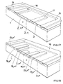
- FIGS. 20 and 21 The finished protective arrangement is shown in FIGS. 20 and 21, specifically FIG. 20 in a sectional view and FIG. 21 in a top view.
- FIGS. 19, 20 and 21 show a protective arrangement in which two Zener diodes act in parallel with one another
- FIGS. 22 and 23 show a protective arrangement in which two Zener diodes are connected in series and these series connections are effective in parallel with one another.
- the semiconductor body of this protective arrangement again consists of a substrate 1 of the p-conductivity type and an epitaxial layer 3 of the n-conductivity type.
- three resistance areas 2 ', 2 ⁇ and 2''' are provided in the form of buried layers.
- a separation zone 23 of the p-conduction type which consists of the regions 23a, 23b, 23c, 23e and 23f, is introduced into the epitaxial layer 3.
- the separation region 23a forms a Zener diode with the resistance region 2 '
- the separation region 23b forms a Zener diode with the resistance region 2'
- the separation region 23c forms with the resistor area 2 '''a Zener diode
- also the separation area 23d forms with the resistance area 2''' a Zener diode.
- the connection zone 27 of the n-line type forms a connection for the resistance area 2 '
- the connection zones 28 and 29 form connections for the resistance area 2 ⁇
- the connection zone 30 of the n-line type forms a connection for the resistance area 2'''.
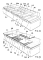
- FIG. 23 shows the finished protective arrangement with the insulating layer 31 on the epitaxial layer 3 and with the electrodes 32, 33, 34 and 35.
- FIG. 24 shows the associated equivalent circuit diagram.
- a protective arrangement according to FIGS. 22, 23 and 24 has the advantage over the protective arrangement according to FIGS. 14, 20 and 21 that the operating voltage for the subsequent circuit to be protected is correspondingly greater due to the series-connected Zener diodes as voltage-limiting element (s) can be chosen.
- FIG. 25 shows a further protective arrangement according to the invention, which again has a substrate 1 of the p-type conduction and an epitaxial layer 3 of the n-conduction type.
- the protective arrangement of FIG. 25 is surrounded by a separation zone 36 of the p-line type.
- a resistance region 2 Between the epitaxial layer 3 and the substrate 1 there is a resistance region 2, which at the same time forms the source zone of a field effect transistor.
- the drain zone of this field effect transistor is formed by an n-type semiconductor zone 37.
- the two p-zones 38 and 39 which form zener diodes with the n-type epitaxial layer 3.
- the p-zone 39 forms the gate electrode of a field effect transi stors.
- connection zone 40 The resistance region 2 or the source zone is contacted by the connection zone 40, while the p-zone 38 is contacted by the connection zone 41 and the p-zone 39 by the connection zone 42.
- the drain zone 37 is contacted by the connection zone 43.
- the connection zones 41 and 42 are connected to the insulation zone 36.
- Figure 26 shows the equivalent circuit of the protective arrangement of Figure 25 with the Zener diode 44, the two substrate diodes 45 and 46, which characterize the pn junction of the resistance zones 2 to the substrate 1, the resistance areas 2 ', 2 ⁇ and 2' '' and the Field effect transistor 47.
- the field effect transistor in the protective arrangement according to FIGS. 25 and 26 has the task of limiting the current occurring at the output of the protective arrangement in the event of a fault, as a result of which the protective function is expanded. This takes place in that when a higher (positive) interference voltage occurs at the source electrode, the channel region K (FIG. 25) of the integrated field effect transistor is cut off.
- the use of a field effect transistor at the output of a protective arrangement according to the invention is also suitable for implementations of protective arrangements which have already been described.
- the resistance of the protective arrangement according to the invention which must absorb the main part of the energy at the limit load and which is characterized, for example, by the sum of the partial resistances 2 ', 2 ⁇ , and 2''' in Figure 16, is preferably dimensioned so that the sum of the voltage drop across this resistor and the value the Zener voltage in the case of the limit load (maximum expected "interference current") does not reach the value of the breakdown voltage for the distance between the connection pad 15 and the area below it, for example oxide layer including n-box.
- the calculation example also shows that Zener diodes with a lower Zener voltage absorb a smaller proportion of the peak energy than those with a higher Zener voltage. If the use of the resistor is provided in the substrate area, as shown in the equivalent circuit according to FIG. 16 with the reference numeral 14, the energy to be converted into heat which occurs in the other areas is correspondingly reduced in the event of a fault. The smaller the proportion of the energy to be converted into heat in the voltage-limiting element (Zener diode), the smaller the area of this element can be made. This means that if a Zener diode is used as a voltage-limiting element, the area, and also the junction capacitance, which, apart from the doping conditions, depends on the junction area, are reduced. This is important if this junction capacitance has a negative influence on the function of the integrated circuit and if the junction area is reduced, this negative influence can be avoided or reduced.
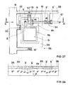
- FIG. 27 shows a development of the invention in which, in addition to a first protective arrangement 48, a second protective arrangement 49 is provided.
- the protective arrangements 48 and 49 in the arrangement according to FIG. 27 are, for example, designs as described with reference to FIGS. 10, 11, 12, 13, 14, 15 and 16.
- the input 5 of the first protective arrangement 48 is connected via the interconnect 8 to the connection pad 15 of the integrated circuit.
- the output connection 6 of the first protective arrangement 48 is via the interconnect 10 with the input 5 'of the second protection arrangement 49, and its output 6' via the interconnect 10 'with the (not shown) circuit arrangement to be protected.
- the interconnect 51 connects the substrate region 50 of the first protective arrangement 48 to the resistance zone 52 of the p-type conduction, while the contact connection zone 53 'is connected to the reference point 16 (ground) of the integrated circuit.
- the substrate area 54 of the second protective arrangement 49 is connected via the interconnect 55 to the reference point 16 of the integrated circuit and at the same time to the reference point of the circuit arrangement (not shown) to be protected.
- the n-zone 56 which is assigned to the connection pad 15, is also included in the substrate region.
- the substrate region 50, in which the first protective arrangement 48 is embedded is “decoupled” from the substrate region 58, in which the second protective arrangement 49 is embedded, by an n-zone 59.
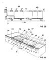
- Figure 28 shows the sectional view of the individual semiconductor zones, based on the section A-A 'of the arrangement of Figure 27 and Figure 30 shows a perspective view.
- FIG. 29 shows the equivalent circuit of the arrangement according to FIG. 27 with the elements of the first protective arrangement 48 and the second protective arrangement 49.
- the mode of operation of the protective arrangements has already been described.
- the equivalent circuit according to FIG. 29 should essentially show the "decoupling" of the substrate areas of the two protective arrangements 48 and 49.
- the substrate region 50 is connected to the reference point 16 of the integrated circuit through the resistors 52 ′ and 52 ⁇ , whereby through an arrangement of the semiconductor zones according to Figure 27, the resistance 52 'is generally smaller than the resistance 52 ⁇ .
- the substrate region 54 of the second protective arrangement 49 can be assigned to the reference point 16 via the line 55, as a result of which the effective resistance between the substrate zone 50 and the reference point 16 can be dimensioned separately.
- the effective resistance between the substrate zone 50 and the reference point 16 can be determined by the design of the resistance zone 52 in FIG. 27.
- the advantage of the arrangement according to the invention according to FIG. 27 is that both the circuit arrangement to be protected, which is connected downstream of the second protection arrangement (49), and the other parts of the integrated circuit, have a greater protective effect because of the "decoupling" of the substrate areas is achieved.
- Another advantage of the arrangement according to FIG. 27 is the possibility, by appropriate dimensioning of the substrate resistance (52 ′, 52 ⁇ ), to choose the proportion of the discharge energy (disturbance) absorbed by this substrate resistance so large that the protective arrangement 48 and 49 corresponds accordingly with regard to the crystal area requirement can be chosen smaller.
- the substrate of the integrated circuit arrangement has the p-line type, but the invention naturally also applies to integrated circuits with a substrate of the n-line type and a correspondingly adapted line type of the other semiconductor zones.
- the resistor provided according to the invention which is provided to protect high-energy electrical disturbances, is, according to FIG. 16, preferably electrically connected to that connection (pin 15, 16) of the integrated circuit arrangement which is affected by the undesired electrical disturbance.
Landscapes
- Semiconductor Integrated Circuits (AREA)
- Metal-Oxide And Bipolar Metal-Oxide Semiconductor Integrated Circuits (AREA)
- Bipolar Integrated Circuits (AREA)
Applications Claiming Priority (2)
| Application Number | Priority Date | Filing Date | Title |
|---|---|---|---|
| DE3714647 | 1987-05-02 | ||
| DE3714647A DE3714647C2 (de) | 1987-05-02 | 1987-05-02 | Integrierte Schaltungsanordnung |
Publications (3)
| Publication Number | Publication Date |
|---|---|
| EP0293575A2 true EP0293575A2 (fr) | 1988-12-07 |
| EP0293575A3 EP0293575A3 (en) | 1990-11-22 |
| EP0293575B1 EP0293575B1 (fr) | 1994-06-22 |
Family
ID=6326697
Family Applications (1)
| Application Number | Title | Priority Date | Filing Date |
|---|---|---|---|
| EP88105515A Expired - Lifetime EP0293575B1 (fr) | 1987-05-02 | 1988-04-07 | Circuit intégré comportant un dispositif de protection |
Country Status (5)
| Country | Link |
|---|---|
| US (1) | US4984031A (fr) |
| EP (1) | EP0293575B1 (fr) |
| JP (1) | JP2823562B2 (fr) |
| KR (1) | KR970003733B1 (fr) |
| DE (2) | DE3714647C2 (fr) |
Families Citing this family (8)
| Publication number | Priority date | Publication date | Assignee | Title |
|---|---|---|---|---|
| US5276350A (en) * | 1991-02-07 | 1994-01-04 | National Semiconductor Corporation | Low reverse junction breakdown voltage zener diode for electrostatic discharge protection of integrated circuits |
| JP3155134B2 (ja) * | 1993-10-27 | 2001-04-09 | ローム株式会社 | 半導体装置 |
| JP3217560B2 (ja) * | 1993-11-15 | 2001-10-09 | 株式会社東芝 | 半導体装置 |
| JP2611639B2 (ja) * | 1993-11-25 | 1997-05-21 | 日本電気株式会社 | 半導体装置 |
| US6111734A (en) * | 1996-03-07 | 2000-08-29 | Dallas Semiconductor Corporation | Electrostatic discharge protection circuits and application |
| US6304126B1 (en) * | 1997-09-29 | 2001-10-16 | Stmicroelectronics S.A. | Protection circuit that can be associated with a filter |
| US6791161B2 (en) | 2002-04-08 | 2004-09-14 | Fabtech, Inc. | Precision Zener diodes |
| KR102576210B1 (ko) * | 2016-07-05 | 2023-09-08 | 삼성전자주식회사 | 반도체 장치 |
Family Cites Families (22)
| Publication number | Priority date | Publication date | Assignee | Title |
|---|---|---|---|---|
| GB1209271A (en) * | 1967-02-27 | 1970-10-21 | Hitachi Ltd | Improvements in semiconductor devices |
| US3562547A (en) * | 1967-04-17 | 1971-02-09 | Ibm | Protection diode for integrated circuit |
| US3619725A (en) * | 1970-04-08 | 1971-11-09 | Rca Corp | Electrical fuse link |
| JPS5191681A (fr) * | 1975-01-22 | 1976-08-11 | ||
| US4042950A (en) * | 1976-03-01 | 1977-08-16 | Advanced Micro Devices, Inc. | Platinum silicide fuse links for integrated circuit devices |
| JPS6112691Y2 (fr) * | 1977-02-08 | 1986-04-19 | ||
| DE2951931C2 (de) * | 1979-12-21 | 1981-10-29 | Siemens AG, 1000 Berlin und 8000 München | Anordnung zum Schutz von bipolaren, integrierten Halbleiterschaltungen vor elektrischen Entladungen |
| JPS5715459A (en) * | 1980-07-01 | 1982-01-26 | Fujitsu Ltd | Semiconductor integrated circuit |
| DE3026361A1 (de) * | 1980-07-11 | 1982-02-04 | Siemens AG, 1000 Berlin und 8000 München | Aus mindestens zwei monolitisch zusammengefassten mis-feldeffekttransistoren bestehender elektrischer widerstand fuer integrierte halbleiterschaltungen |
| US4405933A (en) * | 1981-02-04 | 1983-09-20 | Rca Corporation | Protective integrated circuit device utilizing back-to-back zener diodes |
| US4507756A (en) * | 1982-03-23 | 1985-03-26 | Texas Instruments Incorporated | Avalanche fuse element as programmable device |
| US4491860A (en) * | 1982-04-23 | 1985-01-01 | Signetics Corporation | TiW2 N Fusible links in semiconductor integrated circuits |
| JPS5992557A (ja) * | 1982-11-18 | 1984-05-28 | Nec Corp | 入力保護回路付半導体集積回路 |
| JPS59107555A (ja) * | 1982-12-03 | 1984-06-21 | Fujitsu Ltd | 半導体装置 |
| JPS6196757A (ja) * | 1984-10-17 | 1986-05-15 | Nec Corp | 半導体装置 |
| JPH0732237B2 (ja) * | 1985-04-08 | 1995-04-10 | エスジ−エス−トムソン マイクロエレクトロニクス インコーポレイテッド | 静電放電入力保護回路 |
| JP2580571B2 (ja) * | 1985-07-31 | 1997-02-12 | 日本電気株式会社 | 入力保護回路 |
| GB2179494B (en) * | 1985-08-09 | 1989-07-26 | Plessey Co Plc | Protection structures for integrated circuits |
| JPS6271275A (ja) * | 1985-09-25 | 1987-04-01 | Toshiba Corp | 半導体集積回路 |
| JPS61183550U (fr) * | 1986-04-03 | 1986-11-15 | ||
| JPS63128656A (ja) * | 1986-11-18 | 1988-06-01 | Sanyo Electric Co Ltd | 混成集積回路 |
| JPH0766957B2 (ja) * | 1986-12-12 | 1995-07-19 | 三菱電機株式会社 | 半導体集積回路装置の静電破壊防止装置 |
-
1987
- 1987-05-02 DE DE3714647A patent/DE3714647C2/de not_active Expired - Fee Related
-
1988
- 1988-04-07 EP EP88105515A patent/EP0293575B1/fr not_active Expired - Lifetime
- 1988-04-07 DE DE3850303T patent/DE3850303D1/de not_active Expired - Lifetime
- 1988-04-29 US US07/188,554 patent/US4984031A/en not_active Expired - Fee Related
- 1988-05-02 JP JP63107756A patent/JP2823562B2/ja not_active Expired - Lifetime
- 1988-05-02 KR KR1019880005077A patent/KR970003733B1/ko not_active Expired - Fee Related
Also Published As
| Publication number | Publication date |
|---|---|
| EP0293575B1 (fr) | 1994-06-22 |
| KR970003733B1 (ko) | 1997-03-21 |
| JP2823562B2 (ja) | 1998-11-11 |
| EP0293575A3 (en) | 1990-11-22 |
| US4984031A (en) | 1991-01-08 |
| DE3850303D1 (de) | 1994-07-28 |
| DE3714647A1 (de) | 1988-11-17 |
| JPS63285963A (ja) | 1988-11-22 |
| DE3714647C2 (de) | 1993-10-07 |
| KR880014674A (ko) | 1988-12-24 |
Similar Documents
| Publication | Publication Date | Title |
|---|---|---|
| DE2932152C2 (fr) | ||
| DE19964481B4 (de) | MOS-Halbleiteranordnung mit Schutzeinrichtung unter Verwendung von Zenerdioden | |
| DE69504451T2 (de) | Schutz gegen elektrostatische Entladungen für integrierte Schaltungen | |
| DE60130297T2 (de) | Halbleiterbauelement mit einem ESD-Schutz | |
| DE3505393C2 (de) | Verfahren zum Herstellen eines vertikalen, diffundierten Feldeffekttransistors | |
| DE2257846C3 (de) | Integrierte Halbleiteranordnung zum Schutz gegen Überspannung | |
| DE69221157T2 (de) | Scr-schutzstrukturen und -schutzschaltung mit reduzierten zuendspannung | |
| EP1019964B1 (fr) | Circuit integre a semiconducteur comportant une structure servant a la protection contre des decharges electrostatiques | |
| DE4192215B4 (de) | Halbleiterbauelement mit Temperaturerfassungsschaltung | |
| DE10362232B4 (de) | Leistungshalbleitervorrichtung | |
| DE3145592C2 (fr) | ||
| DE69232257T2 (de) | Durch Verarmung kontrollierte Isolationsstufe | |
| DE10322593A1 (de) | Halbleiterbauteil und dieses verwendender integrierter Schaltkreis | |
| DE19654163B4 (de) | Schutzvorrichtung für eine Halbleiterschaltung | |
| CH668505A5 (de) | Halbleiterbauelement. | |
| DE3428067C2 (de) | Halbleiter-Überspannungsunterdrücker mit genau vorherbestimmbarer Einsatzspannung und Verfahren zur Herstellung desselben | |
| DE69302244T2 (de) | Halbleiter-Schutzkomponente | |
| DE3688034T2 (de) | Vor elektrostatischen entladungen geschuetzte eingangsschaltung. | |
| EP0099897A1 (fr) | Circuit darlington a transistors. | |
| DE69320749T2 (de) | Strommessschaltung | |
| EP0293575B1 (fr) | Circuit intégré comportant un dispositif de protection | |
| EP0098834B1 (fr) | Dispositif semi-conducteur planaire | |
| DE69022726T2 (de) | Scr-schutzanordnung mit niedriger zündspannung und struktur. | |
| DE2329398B2 (de) | In Ruckwartsrichtung leitendes Thyristorbauelement | |
| EP0017980B1 (fr) | Thyristor contrôlé par un transistor à effet de champ |
Legal Events
| Date | Code | Title | Description |
|---|---|---|---|
| PUAI | Public reference made under article 153(3) epc to a published international application that has entered the european phase |
Free format text: ORIGINAL CODE: 0009012 |
|
| AK | Designated contracting states |
Kind code of ref document: A2 Designated state(s): DE FR GB IT NL |
|
| PUAL | Search report despatched |
Free format text: ORIGINAL CODE: 0009013 |
|
| AK | Designated contracting states |
Kind code of ref document: A3 Designated state(s): DE FR GB IT NL |
|
| 17P | Request for examination filed |
Effective date: 19910513 |
|
| 17Q | First examination report despatched |
Effective date: 19920518 |
|
| RAP1 | Party data changed (applicant data changed or rights of an application transferred) |
Owner name: TEMIC TELEFUNKEN MICROELECTRONIC GMBH |
|
| GRAA | (expected) grant |
Free format text: ORIGINAL CODE: 0009210 |
|
| AK | Designated contracting states |
Kind code of ref document: B1 Designated state(s): DE FR GB IT NL |
|
| ITF | It: translation for a ep patent filed | ||
| GBT | Gb: translation of ep patent filed (gb section 77(6)(a)/1977) |
Effective date: 19940628 |
|
| REF | Corresponds to: |
Ref document number: 3850303 Country of ref document: DE Date of ref document: 19940728 |
|
| ET | Fr: translation filed | ||
| PLBE | No opposition filed within time limit |
Free format text: ORIGINAL CODE: 0009261 |
|
| STAA | Information on the status of an ep patent application or granted ep patent |
Free format text: STATUS: NO OPPOSITION FILED WITHIN TIME LIMIT |
|
| 26N | No opposition filed | ||
| PGFP | Annual fee paid to national office [announced via postgrant information from national office to epo] |
Ref country code: NL Payment date: 19990427 Year of fee payment: 12 |
|
| NLS | Nl: assignments of ep-patents |
Owner name: TEMIC SEMICONDUCTOR GMBH |
|
| REG | Reference to a national code |
Ref country code: GB Ref legal event code: 732E |
|
| REG | Reference to a national code |
Ref country code: FR Ref legal event code: TP |
|
| PG25 | Lapsed in a contracting state [announced via postgrant information from national office to epo] |
Ref country code: NL Free format text: LAPSE BECAUSE OF NON-PAYMENT OF DUE FEES Effective date: 20001101 |
|
| NLV4 | Nl: lapsed or anulled due to non-payment of the annual fee |
Effective date: 20001101 |
|
| PGFP | Annual fee paid to national office [announced via postgrant information from national office to epo] |
Ref country code: GB Payment date: 20010316 Year of fee payment: 14 |
|
| REG | Reference to a national code |
Ref country code: GB Ref legal event code: IF02 |
|
| PG25 | Lapsed in a contracting state [announced via postgrant information from national office to epo] |
Ref country code: GB Free format text: LAPSE BECAUSE OF NON-PAYMENT OF DUE FEES Effective date: 20020407 |
|
| PGFP | Annual fee paid to national office [announced via postgrant information from national office to epo] |
Ref country code: FR Payment date: 20020927 Year of fee payment: 15 |
|
| GBPC | Gb: european patent ceased through non-payment of renewal fee |
Effective date: 20020407 |
|
| PG25 | Lapsed in a contracting state [announced via postgrant information from national office to epo] |
Ref country code: FR Free format text: LAPSE BECAUSE OF NON-PAYMENT OF DUE FEES Effective date: 20031231 |
|
| REG | Reference to a national code |
Ref country code: FR Ref legal event code: ST |
|
| PG25 | Lapsed in a contracting state [announced via postgrant information from national office to epo] |
Ref country code: IT Free format text: LAPSE BECAUSE OF NON-PAYMENT OF DUE FEES;WARNING: LAPSES OF ITALIAN PATENTS WITH EFFECTIVE DATE BEFORE 2007 MAY HAVE OCCURRED AT ANY TIME BEFORE 2007. THE CORRECT EFFECTIVE DATE MAY BE DIFFERENT FROM THE ONE RECORDED. Effective date: 20050407 |
|
| PGFP | Annual fee paid to national office [announced via postgrant information from national office to epo] |
Ref country code: DE Payment date: 20070423 Year of fee payment: 20 |