EP0290345B1 - Film électroconducteur pour élément photovoltaique - Google Patents
Film électroconducteur pour élément photovoltaique Download PDFInfo
- Publication number
- EP0290345B1 EP0290345B1 EP88401097A EP88401097A EP0290345B1 EP 0290345 B1 EP0290345 B1 EP 0290345B1 EP 88401097 A EP88401097 A EP 88401097A EP 88401097 A EP88401097 A EP 88401097A EP 0290345 B1 EP0290345 B1 EP 0290345B1
- Authority
- EP
- European Patent Office
- Prior art keywords
- film
- layer
- sno2
- layers
- electrically conducting
- Prior art date
- Legal status (The legal status is an assumption and is not a legal conclusion. Google has not performed a legal analysis and makes no representation as to the accuracy of the status listed.)
- Expired - Lifetime
Links
Images

Classifications
-
- H—ELECTRICITY
- H10—SEMICONDUCTOR DEVICES; ELECTRIC SOLID-STATE DEVICES NOT OTHERWISE PROVIDED FOR
- H10F—INORGANIC SEMICONDUCTOR DEVICES SENSITIVE TO INFRARED RADIATION, LIGHT, ELECTROMAGNETIC RADIATION OF SHORTER WAVELENGTH OR CORPUSCULAR RADIATION
- H10F77/00—Constructional details of devices covered by this subclass
- H10F77/20—Electrodes
- H10F77/244—Electrodes made of transparent conductive layers, e.g. transparent conductive oxide [TCO] layers
-
- H—ELECTRICITY
- H10—SEMICONDUCTOR DEVICES; ELECTRIC SOLID-STATE DEVICES NOT OTHERWISE PROVIDED FOR
- H10F—INORGANIC SEMICONDUCTOR DEVICES SENSITIVE TO INFRARED RADIATION, LIGHT, ELECTROMAGNETIC RADIATION OF SHORTER WAVELENGTH OR CORPUSCULAR RADIATION
- H10F71/00—Manufacture or treatment of devices covered by this subclass
- H10F71/138—Manufacture of transparent electrodes, e.g. transparent conductive oxides [TCO] or indium tin oxide [ITO] electrodes
-
- Y—GENERAL TAGGING OF NEW TECHNOLOGICAL DEVELOPMENTS; GENERAL TAGGING OF CROSS-SECTIONAL TECHNOLOGIES SPANNING OVER SEVERAL SECTIONS OF THE IPC; TECHNICAL SUBJECTS COVERED BY FORMER USPC CROSS-REFERENCE ART COLLECTIONS [XRACs] AND DIGESTS
- Y02—TECHNOLOGIES OR APPLICATIONS FOR MITIGATION OR ADAPTATION AGAINST CLIMATE CHANGE
- Y02E—REDUCTION OF GREENHOUSE GAS [GHG] EMISSIONS, RELATED TO ENERGY GENERATION, TRANSMISSION OR DISTRIBUTION
- Y02E10/00—Energy generation through renewable energy sources
- Y02E10/50—Photovoltaic [PV] energy
Definitions
- the present invention relates to a transparent electroconductive film with two layers composed mainly of tin oxide. More specifically, it relates to a transparent electroconductive film for solar cells.
- An inexpensive solar cell consisting of a photovoltaic converter element in amorphous silicon (a-Si) deposited on a transparent electroconductive substrate with aluminum electrodes is known.
- a-Si amorphous silicon
- Such an a-Si solar cell has a lower efficiency in photovoltaic conversion than other solar cells having a crystalline semiconductor.
- SnO Sn layer F
- F fluorine-doped tin oxide layer
- the Japanese patent document published under the number 62-211966 proposes to use as transparent electrode deposited on a substrate a transparent electroconductive film with two layers (hereinafter "2-layer film SnO2: Cl - SnO2: F ”) consisting of a surface layer of tin oxide having no halogen other than chlorine (hereinafter called" SnO2 layer: Cl ”) and an underlying layer of tin doped with fluorine (hereinafter referred to as "SnO2 layer: F) deposited directly on the transparent substrate.
- 2-layer film SnO2: Cl - SnO2: F consisting of a surface layer of tin oxide having no halogen other than chlorine
- SnO2 layer: F an underlying layer of tin doped with fluorine
- the ratio of the thickness of the fluorine-doped tin oxide layer at the thickness of the entire two-layer transparent film is less than 50%, it is possible to obtain a transparent electroconductive film with a lower surface resistance than in the case of a film in a single layer of SnO2: Cl of the same overall thickness and of a higher transmission than in the case of a film in a single layer of SnO2: F of the same overall thickness. Consequently, in the case of the use of a film with 2 layers SnO2: Cl / SnO2: F as transparent electrode, the yield in photovoltaic conversion of a solar cell is improved, compared to the case in which a film is used. with a single layer of SnO2: Cl or SnO2: F.
- the SnO2: Cl layer has a higher surface resistance than the SnO2: F layer, in the case of a solar cell employing as a transparent electrode a film with two layers, the surface layer of which is a layer of SnO2 : Cl, the improvement of the yield in photovoltaic conversion is limited.
- the present invention aims to solve the aforementioned problem.
- the layer composed mainly of tin oxide and containing no fluorine is a layer SnO2: Cl, that is to say a layer containing no halogen except chlorine obtained from a tin compound containing no halogen except chlorine or a non-chlorine tin compound to which a chlorine supplier such as HCl is added.
- the substrate is heated, it is brought into contact with the compound of chlorinated tin or without chlorine or any other halogen, but with an addition of Cl carrier, which makes it possible to obtain the first layer SnO2: Cl.
- the partially coated substrate is again heated and brought into contact with a fluorinated tin compound or with a tin compound and a fluorinated compound to obtain the second layer SnO2: F.
- C4H9S n Cl3, SnCl4, (CH3) 2SnCl2, etc. among the chlorinated compounds, and mention may be made of (CnH 2n + 1 ) 4Sn with n 1 to 4, (CH3) 2SnH2, (C4H9) 3SnH, (C4H9) 2Sn (COOCH3) 2, etc., as chlorine-free compounds which are supplemented with a chlorine supplier such as HCL.
- F layer all of the aforementioned tin compounds can be used, provided that a fluorine donor is added: CH3CH2F2, CHClF2, CH3CCLF2, CHF3, CF2Cl2, CF3Cl, CF3Br.
- CVD method chemical gas deposition method
- the CVD method is used by which a mixture of vapor of tin compounds, oxidizing gas, etc. is brought into contact with the transparent substrate heated to a temperature of 400 to 600 ° C.
- a transparent electroconductive film with two layers is thus deposited, that is to say, a layer SnO2: Cl then another layer SnO2: F, deposited in overlap.
- the thickness of the film with two layers SnO2: F / SnO2: Cl is 0.6 to 1.0 micron.
- the ratio of the thickness of the SnO2: F layer to that of the entire film is more than 5%, but less than 50%, and preferably more than 10%.
- the photovoltaic conversion efficiency drops significantly.
- the transparent surface electroconductive layer is a SnO2: F layer
- the transparent electroconductive film whose light transmission is identical to that of a film with two SnO Sn: Cl / SnO2: F layers of the same total thickness. and having the same thickness ratio of the layer SnO2: F with respect to the total thickness, but for which the order of the layers is reversed, but whose electrical surface resistance is lower.
- the photovoltaic conversion efficiency can be improved. So for example we made samples and compared performance.
- a SnO2: Cl layer was deposited by CVD on the glass substrates heated to 550 ° C. Then, these glass substrates coated with this SnO2: Cl layer were heated to 550 ° C. and deposited by CVD another SnO2: F layer on the first layer of tin oxide having no halogen other than chlorine using a mixture of monobutyl tin trichloride vapor, water vapor, oxygen, 1,2-difluoroethane and nitrogen, a SnO2: F / SnO2: Cl film was thus obtained.
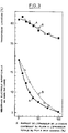
- FIG. 3 shows the results of these measurements. From FIG. 3, it is clear that the transmissions of "A” and that of "B” are identical for identical values of x and that the surface electrical resistance of "A” is lower than that of "B "for the same value of x.
- the invention can be applied to make solar cells, but also for other photovoltaic applications.
Landscapes
- Photovoltaic Devices (AREA)
- Laminated Bodies (AREA)
- Non-Insulated Conductors (AREA)
- Physical Vapour Deposition (AREA)
Description
- La présente invention concerne un film électroconducteur transparent à deux couches composées principalement d'oxyde d'étain. Plus précisément, elle porte sur un film électroconducteur transparent pour pile solaire.
- Une pile solaire bon marché constituée d'un élément convertisseur photovoltaïque en silicium amorphe (a-Si) déposé sur un substrat électroconducteur transparent avec des électrodes en aluminium est connue. Une telle pile solaire à a-Si a un plus faible rendement en conversion photovoltaïque que d'autres piles solaires ayant un semi-conducteur cristallin.
- Pour l'améliorer, plusieurs mesures sont possibles. L'une consiste à augmenter au maximum la transmission de l'électrode transparente vis-à-vis de la lumière incidente et de réduire la résistance électrique de surface. Comme couche électroconductrice transparente à faible résistance de surface, une couche d'oxyde d'étain dopée au fluor (désignée ci-après "couche SnO₂:F") a déjà été proposée. Toutefois le dopage de la couche d'oxyde d'étain avec le fluor fait diminuer sa capacité de transmission de la lumière. Donc ce dopage apparaît comme un inconvénient si l'on veut obtenir une couche électroconductrice transparente à faible résistance électrique et en même temps des performances élevées en transmission.
- Pour résoudre ce problème, le document de brevet japonais publié sous le n° 62-211966 propose d'utiliser comme électrode transparente déposée sur un substrat un film électroconducteur transparent à deux couches (désigné ci-après "film à 2 couches SnO₂:Cl - SnO₂:F") constitué d'une couche superficielle d'oxyde d'étain n'ayant pas d'halogène autre que le chlore (désigné ci-après "couche SnO₂:Cl") et d'une couche sous jacente d'étain dopé au fluor (désigné ci-après "couche SnO₂:F) déposée directement sur le substrat transparent. Du fait que le rapport de l'épaisseur de la couche d'oxyde d'étain dopé au fluor à l'épaisseur de la totalité du film transparent à deux couches est inférieur à 50%, on peut obtenir un film électroconducteur transparent d'une plus faible résistance de surface que dans le cas d'un film en une seule couche de SnO₂:Cl de même épaisseur globale et d'une plus haute transmission que dans le cas d'un film en une seule couche de SnO₂:F de même épaisseur globale. Par conséquent, dans le cas de l'emploi d'un film à 2 couches SnO₂:Cl/SnO₂:F comme électrode transparente, le rendement en conversion photovoltaïque d'une pile solaire est amélioré, comparé au cas dans lequel on emploie un film à une seule couche de SnO₂:Cl ou de SnO₂:F.
- Toutefois, du fait que la couche SnO₂:Cl a une plus grande résistance de surface que la couche SnO₂:F, dans le cas d'une pile solaire employant comme électrode transparente un film à deux couches dont la couche superficielle est une couche de SnO₂:Cl, l'amélioration du rendement en conversion photovoltaïque est limitée.
- Par ailleurs, il est connu de la demande de brevet EP-A-0 234 222, déposée le 14 janvier 1987 sous priorité du 25 février 1986 et publiée le 2 septembre 1987, un film électroconducteur composé d'une première couche d'oxyde d'étain non dopé déposée sur un substrat transparent et surmontée d'une seconde couche d'oxyde d'étain dopé par des impuretés comme du fluor, du chlore ou de l'antimoine.
- La présente invention vise à résoudre le problème précité.
- Elle a également pour but de fournir un film électroconducteur transparent pour élément photovoltaïque apte à augmenter le rendement de conversion photovoltaïque. Ces buts sont atteints au moyen d'un film tel que defini dans les jeux de revendications pour les états désignés DE, FR, GB et pour les états désignés BE, ES, IT, NL, SE.
- Avantageusement la couche composée principalement d'oxyde d'étain et ne contenant pas de fluor est une couche SnO₂:Cl, c'est-à-dire une couche ne contenant pas d'halogène sauf du chlore obtenue à partir d'un composé d'étain contenant aucun halogène sauf du chlore ou d'un composé d'étain sans chlore auquel on ajoute un apporteur de chlore tel HCl.
- L'invention sera maintenant décrite plus en détail en référence aux figures jointes qui représentent :
- . figure 1 : un film à deux couches conforme à l'invention déposé sur un substrat,
- . figure 2 : un film à deux couches, classique,
- . figure 3 : un graphique montrant pour différents films classiques et selon l'invention, les valeurs des caractéristiques de transmission lumineuse et de résistance électrique superficielle, cela pour différents valeurs du rapport X de l'épaisseur de la couche SnO₂:F à l'épaisseur totale du film.
- Pour réaliser le dépôt du film à deux couches, on chauffe le substrat, on le met en contact avec le composé d'étain chloré ou sans chlore ni aucun autre halogène, mais avec un appoint d'apporteur de Cl, ce qui permet d'obtenir la première couche SnO₂:Cl. Puis on chauffe à nouveau le substrat partiellement revêtu et on le met en contact avec un composé d'étain fluoré ou avec un composé d'étain et un composé fluoré pour obtenir la seconde couche SnO₂:F.
- Comme composés d'étain utilisables pour le dépôt de la couche SnO₂:Cl, on peut citer C₄H₉SnCl₃, SnCl₄, (CH₃)₂SnCl₂, etc parmi les composés chlorés, et on peut citer (CnH2n+1)₄Sn avec n = 1 à 4, (CH₃)₂SnH₂, (C₄H₉)₃SnH, (C₄H₉)₂Sn(COOCH₃)₂, etc, comme composés sans chlore auxquels on fait un appoint avec un apporteur de chlore tel HCL.
- Pour déposer la couche SnO₂:F, on peut utiliser tous les composés d'étain précités à condition de faire un appoint de donneur de fluor : CH₃CH₂F₂, CHClF₂, CH₃CCLF₂, CHF₃, CF₂Cl₂, CF₃Cl, CF₃Br.
- Pour mettre ces composés d'étain en contact avec des substrats transparents chauffés et pour provoquer l'oxydation et la décomposition thermique, on utilise la méthode de dépôt chimique en phase gazeuse (méthode CVD) par laquelle on met une vapeur de composés d'étain et un gaz oxydant en contact avec un substrat transparent à haute température, ou bien la méthode de pulvérisation par laquelle on pulvérise une solution du composé d'étain, sur le substrat transparent à haute température à l'aide d'un pulvérisateur.
- On utilise de préférence la méthode CVD par laquelle on met un mélange de vapeur de composés d'étain, de gaz oxydant, etc... en contact avec le substrat transparent chauffé à une température de 400 à 600°C. On dépose ainsi un film électroconducteur transparent à deux couches, c'est-à-dire, une couche SnO₂:Cl puis une autre couche SnO₂:F, déposée en recouvrement.
- Selon la présente invention, l'épaisseur du film à deux couches SnO₂:F/SnO₂:Cl est de 0.6 à 1.0 micron. Toutefois, pour améliorer le rendement de conversion photovoltaïque, il est préférable que le rapport de l'épaisseur de la couche SnO₂:F sur celle de la totalité du film soit de plus de 5%, mais toutefois inférieure à 50%, et de préférence, de plus de 10%. Quand le rapport d'épaisseur précité est inférieur à 5%, le rendement de conversion photovoltaïque baisse sensiblement.
- Du fait que la couche électroconductrice transparente superficielle est une couche SnO₂:F, on peut obtenir un film électroconducteur transparent dont la transmission lumineuse est identique à celle d'un film à deux couches SnO₂:Cl/SnO₂:F d'une même épaisseur totale et ayant un même rapport d'épaisseur de la couche SnO₂:F vis-à-vis de l'épaisseur totale, mais pour lequel l'ordre des couches est inversé, mais dont la résistance électrique superficielle est plus faible. Il en résulte qu'on peut améliorer le rendement de conversion photovoltaïque. Ainsi par exemple on a fabriqué des échantillons et on a comparé les performances.
- On a bien lavé et séché des plaques de verre à base de soude et de chaux revêtues d'une couche d'oxyde de silicium, d'une taille de 25 mm x 30 mm et d'une épaisseur de 1.1 mm. On les a utilisées comme substrats de verre. Puis, on a déposé un film électroconducteur transparent sur ces substrats de verre selon les procédés suivants.
- En utilisant un mélange de vapeur de monobutyle trichlorure d'étain, de vapeur d'eau, d'oxygène et d'azote, on a déposé par CVD une couche SnO₂:Cl sur les substrats de verre chauffés à 550°C. Puis, on a chauffé à 550° C ces substrats de verre revêtus de cette couche SnO₂:Cl et déposé par CVD une autre couche SnO₂:F sur la première couche d'oxyde d'étain n'ayant pas d'halogène autre que le chlore en utilisant un mélange de vapeur de monobutyle trichlorure d'étain, de vapeur d'eau, d'oxygène, de 1,2-difluoroéthane et d'azote, on a ainsi obtenu un film SnO₂:F/SnO₂:Cl.
- Sur la figure 1, on indique la structure d'un tel film électroconducteur transparent deux couches SnO₂:F.SnO₂:Cl. 1 est la référence du substrat en verre, 2 est la couche SnO₂:Cl, 3 est la couche SnO₂:F.
- En changeant la durée de dépôt de chacune des couches SnO₂:Cl et SnO₂:F et en conservant toujours une épaisseur totale du film à deux couches de 0,85 micron, on a obtenu des rapports x de l'épaisseur de la couche SnO₂:F sur l'épaisseur de la totalité du film, qui étaient de 0, 9, 18.5, 27, 36, 49.5, 73 et 100 %. Ces échantillons sont désignés "A".
- A titre comparatif, on a déposé des films à deux couches SnO₂:Cl/SnO₂:F, c'est-à-dire ayant la structure inversée. On a obtenu 5 échantillons pour lesquels les rapports d'épaisseur x précités étaient de 15, 26.5, 50, 65 et 76%. Ces échantillons sont désignés "B".
- On a mesuré la transmission du rayonnement visible et la résistance électrique de surface des ces échantillons A et B. Sur la figure 3, on indique les résultats de ces mesures. D'après la figure 3, il est clair que les transmissions de "A" et celle de "B" sont identiques pour des valeurs de x identiques et que la résistance électrique de surface de "A" est plus faible que celle de "B" pour une même valeur de x.
- Il en résulte que selon la présente invention, on peut obtenir des films électroconducteurs transparents de faible résistance électrique et autorisant une importante transmission lumineuse.
- L'invention peut être appliquée pour réaliser des piles solaires, mais également pour d'autres applications photovoltaïques.
Claims (6)
- Film électroconducteur transparent à deux couches (2, 3), caractérisé en ce qu'il est constitué d'une couche électroconductrice transparente (3) composée principalement d'oxyde d'étain comprenant du fluor déposée au-dessus d'une autre couche électroconductrice transparente (2) étant composée principalement d'oxyde d'étain ne comprenant pas de fluor ni d'halogène autre que le chlore et étant déposée au-dessus d'un substrat transparent (1).
- Film électroconducteur transparent à deux couches (2, 3) selon la revendication 1, caractérisé en ce que l'épaisseur de ce film est de 0,6 micron à 1,0 micron.
- Film électroconducteur transparent à deux couches (2, 3) selon la revendication 2, caractérisé en ce que le rapport x de l'épaisseur de la couche (3) composée principalement d'oxyde d'étain comprenant du fluor à l'épaisseur totale du film à deux couches (2, 3) est supérieur ou égal à 5 % et inférieur à 50 %.
- Film électroconducteur transparent à deux couches (2, 3) selon la revendication 3, caractérisé en ce que le rapport x est supérieur à 10 %.
- Application du film selon l'une des revendications précédentes à la réalisation de piles solaires et en général d'éléments photovoltaïques.
Applications Claiming Priority (2)
| Application Number | Priority Date | Filing Date | Title |
|---|---|---|---|
| JP62111471A JPH07112076B2 (ja) | 1987-05-07 | 1987-05-07 | 二層構造を有する透明導電膜体 |
| JP111471/87 | 1987-05-07 |
Publications (3)
| Publication Number | Publication Date |
|---|---|
| EP0290345A2 EP0290345A2 (fr) | 1988-11-09 |
| EP0290345A3 EP0290345A3 (en) | 1989-04-26 |
| EP0290345B1 true EP0290345B1 (fr) | 1994-09-07 |
Family
ID=14562087
Family Applications (1)
| Application Number | Title | Priority Date | Filing Date |
|---|---|---|---|
| EP88401097A Expired - Lifetime EP0290345B1 (fr) | 1987-05-07 | 1988-05-05 | Film électroconducteur pour élément photovoltaique |
Country Status (6)
| Country | Link |
|---|---|
| EP (1) | EP0290345B1 (fr) |
| JP (1) | JPH07112076B2 (fr) |
| BR (1) | BR8802239A (fr) |
| CA (1) | CA1310865C (fr) |
| DE (1) | DE3851361T2 (fr) |
| ES (1) | ES2063762T3 (fr) |
Families Citing this family (4)
| Publication number | Priority date | Publication date | Assignee | Title |
|---|---|---|---|---|
| DE69904137T2 (de) | 1999-02-26 | 2004-03-18 | Agfa-Gevaert | Schicht auf Basis eines leitfähigen Metalloxids |
| JP2003060216A (ja) * | 2001-08-10 | 2003-02-28 | Nippon Sheet Glass Co Ltd | 光電変換装置用基板 |
| EP1635361B1 (fr) * | 2003-06-17 | 2016-08-17 | Nippon Sheet Glass Company, Limited | Procédé de fabrication d'un convertisseur photoélectrique avec substrat conducteur transparent |
| KR20080074086A (ko) * | 2005-11-17 | 2008-08-12 | 아사히 가라스 가부시키가이샤 | 태양 전지용 투명 도전성 기판 및 그 제조 방법 |
Family Cites Families (7)
| Publication number | Priority date | Publication date | Assignee | Title |
|---|---|---|---|---|
| FR2439240A1 (fr) * | 1978-10-20 | 1980-05-16 | Gordon Roy Gerald | Procede pour produire des pellicules transparentes d'oxyde stannique sur un substrat chauffe, leur utilisation pour fabriquer des produits comportant une telle pellicule et appareil pour la mise en oeuvre de ce procede |
| US4338482A (en) * | 1981-02-17 | 1982-07-06 | Roy G. Gordon | Photovoltaic cell |
| JPS60211817A (ja) * | 1984-04-05 | 1985-10-24 | Semiconductor Energy Lab Co Ltd | 光電変換装置 |
| JPH064497B2 (ja) * | 1985-08-05 | 1994-01-19 | 日本板硝子株式会社 | 酸化錫膜の形成方法 |
| JPS6269405A (ja) * | 1985-09-20 | 1987-03-30 | 日本板硝子株式会社 | 光電素子用透明導電基板 |
| JPH0664935B2 (ja) * | 1985-10-18 | 1994-08-22 | ティーディーケイ株式会社 | 透明導電膜およびその形成方法 |
| JPS62198169A (ja) * | 1986-02-25 | 1987-09-01 | Fuji Electric Corp Res & Dev Ltd | 太陽電池 |
-
1987
- 1987-05-07 JP JP62111471A patent/JPH07112076B2/ja not_active Expired - Lifetime
-
1988
- 1988-05-05 ES ES88401097T patent/ES2063762T3/es not_active Expired - Lifetime
- 1988-05-05 EP EP88401097A patent/EP0290345B1/fr not_active Expired - Lifetime
- 1988-05-05 DE DE3851361T patent/DE3851361T2/de not_active Expired - Fee Related
- 1988-05-06 CA CA000566080A patent/CA1310865C/fr not_active Expired - Fee Related
- 1988-05-06 BR BR8802239A patent/BR8802239A/pt not_active IP Right Cessation
Non-Patent Citations (1)
| Title |
|---|
| THIN SOLID FILMS vol. 113, no. 2, mars 1984, pages 93 - 100, Lausanne, CH; G. MMAVRODIEV et al.: "Properties of Sn02:F Films Prepared on Glass Substrates by the Spraying Method" * |
Also Published As
| Publication number | Publication date |
|---|---|
| DE3851361T2 (de) | 1995-05-11 |
| JPH07112076B2 (ja) | 1995-11-29 |
| DE3851361D1 (de) | 1994-10-13 |
| BR8802239A (pt) | 1988-12-06 |
| ES2063762T3 (es) | 1995-01-16 |
| EP0290345A2 (fr) | 1988-11-09 |
| JPS63275187A (ja) | 1988-11-11 |
| EP0290345A3 (en) | 1989-04-26 |
| CA1310865C (fr) | 1992-12-01 |
Similar Documents
| Publication | Publication Date | Title |
|---|---|---|
| JP4537000B2 (ja) | 電極を備えた透明基材 | |
| US5797999A (en) | Solar cell and method for fabricating the same | |
| US4338482A (en) | Photovoltaic cell | |
| WO2009156640A2 (fr) | Cellule photovoltaïque et substrat de cellule photovoltaïque | |
| EP0115645B1 (fr) | Procédé pour la formation d'une couche de passivation sur un dispositif de conversion photoélectrique et dispositif obtenu selon ce procédé | |
| WO2008105597A1 (fr) | Électrode transparente pour pile solaire et procédé de fabrication associé | |
| US8187714B2 (en) | Transparent substrate provided with an electrode | |
| JPH0656883B2 (ja) | 半導体装置 | |
| US4485265A (en) | Photovoltaic cell | |
| JPH07105166B2 (ja) | フッ素ドープ酸化錫膜及びその低抵抗化方法 | |
| JP3616824B2 (ja) | pin型光電変換素子及び製造方法 | |
| EP0290345A2 (fr) | Film électroconducteur pour élément photovoltaique | |
| WO2010001013A2 (fr) | Cellule photovoltaïque et substrat de cellule photovoltaïque | |
| JPH06163955A (ja) | 太陽電池用基板及び太陽電池 | |
| US5064477A (en) | Radiant energy sensitive device and method | |
| EP0382632B1 (fr) | Substrat transparent électroconducteur à deux couches d'oxydes métalliques, utile notamment dans des dispositifs opto-électroniques | |
| US5278015A (en) | Amorphous silicon film, its production and photo semiconductor device utilizing such a film | |
| EP0216703B1 (fr) | Substrat conducteur et transparent pour élément photoélectrique | |
| US5152833A (en) | Amorphous silicon film, its production and photo semiconductor device utilizing such a film | |
| US4234353A (en) | Process for preparing photovoltaic cells having increased adhesion of the semi-conducting layer and produced thereby to the conducting layer | |
| JPS58111379A (ja) | 薄膜太陽電池 | |
| JP3146612B2 (ja) | 固溶体薄膜の製造方法および太陽電池の製造方法 | |
| JP3382141B2 (ja) | 光電変換素子 | |
| JPS6152992B2 (fr) | ||
| JPH11298021A (ja) | 光起電力素子用基板、これを用いた光起電力素子及び集積型光起電力素子並びに集積型光起電力素子の製造方法 |
Legal Events
| Date | Code | Title | Description |
|---|---|---|---|
| PUAI | Public reference made under article 153(3) epc to a published international application that has entered the european phase |
Free format text: ORIGINAL CODE: 0009012 |
|
| AK | Designated contracting states |
Kind code of ref document: A2 Designated state(s): BE DE ES FR GB IT NL SE |
|
| PUAL | Search report despatched |
Free format text: ORIGINAL CODE: 0009013 |
|
| AK | Designated contracting states |
Kind code of ref document: A3 Designated state(s): BE DE ES FR GB IT NL SE |
|
| 17P | Request for examination filed |
Effective date: 19890920 |
|
| RAP1 | Party data changed (applicant data changed or rights of an application transferred) |
Owner name: SAINT-GOBAIN VITRAGE INTERNATIONAL |
|
| 17Q | First examination report despatched |
Effective date: 19930107 |
|
| GRAA | (expected) grant |
Free format text: ORIGINAL CODE: 0009210 |
|
| AK | Designated contracting states |
Kind code of ref document: B1 Designated state(s): BE DE ES FR GB IT NL SE |
|
| REF | Corresponds to: |
Ref document number: 3851361 Country of ref document: DE Date of ref document: 19941013 |
|
| ITF | It: translation for a ep patent filed | ||
| GBT | Gb: translation of ep patent filed (gb section 77(6)(a)/1977) |
Effective date: 19941213 |
|
| REG | Reference to a national code |
Ref country code: ES Ref legal event code: FG2A Ref document number: 2063762 Country of ref document: ES Kind code of ref document: T3 |
|
| EAL | Se: european patent in force in sweden |
Ref document number: 88401097.6 |
|
| PLBE | No opposition filed within time limit |
Free format text: ORIGINAL CODE: 0009261 |
|
| STAA | Information on the status of an ep patent application or granted ep patent |
Free format text: STATUS: NO OPPOSITION FILED WITHIN TIME LIMIT |
|
| 26N | No opposition filed | ||
| REG | Reference to a national code |
Ref country code: GB Ref legal event code: IF02 |
|
| PGFP | Annual fee paid to national office [announced via postgrant information from national office to epo] |
Ref country code: GB Payment date: 20020501 Year of fee payment: 15 |
|
| PGFP | Annual fee paid to national office [announced via postgrant information from national office to epo] |
Ref country code: SE Payment date: 20020508 Year of fee payment: 15 |
|
| PGFP | Annual fee paid to national office [announced via postgrant information from national office to epo] |
Ref country code: FR Payment date: 20020515 Year of fee payment: 15 |
|
| PGFP | Annual fee paid to national office [announced via postgrant information from national office to epo] |
Ref country code: ES Payment date: 20020522 Year of fee payment: 15 |
|
| PGFP | Annual fee paid to national office [announced via postgrant information from national office to epo] |
Ref country code: NL Payment date: 20020529 Year of fee payment: 15 |
|
| PGFP | Annual fee paid to national office [announced via postgrant information from national office to epo] |
Ref country code: BE Payment date: 20020530 Year of fee payment: 15 |
|
| PGFP | Annual fee paid to national office [announced via postgrant information from national office to epo] |
Ref country code: DE Payment date: 20020610 Year of fee payment: 15 |
|
| PG25 | Lapsed in a contracting state [announced via postgrant information from national office to epo] |
Ref country code: GB Free format text: LAPSE BECAUSE OF NON-PAYMENT OF DUE FEES Effective date: 20030505 |
|
| PG25 | Lapsed in a contracting state [announced via postgrant information from national office to epo] |
Ref country code: SE Free format text: LAPSE BECAUSE OF NON-PAYMENT OF DUE FEES Effective date: 20030506 Ref country code: ES Free format text: LAPSE BECAUSE OF NON-PAYMENT OF DUE FEES Effective date: 20030506 |
|
| PG25 | Lapsed in a contracting state [announced via postgrant information from national office to epo] |
Ref country code: BE Free format text: LAPSE BECAUSE OF NON-PAYMENT OF DUE FEES Effective date: 20030531 |
|
| BERE | Be: lapsed |
Owner name: *SAINT-GOBAIN VITRAGE INTERNATIONAL Effective date: 20030531 |
|
| PG25 | Lapsed in a contracting state [announced via postgrant information from national office to epo] |
Ref country code: NL Free format text: LAPSE BECAUSE OF NON-PAYMENT OF DUE FEES Effective date: 20031201 |
|
| PG25 | Lapsed in a contracting state [announced via postgrant information from national office to epo] |
Ref country code: DE Free format text: LAPSE BECAUSE OF NON-PAYMENT OF DUE FEES Effective date: 20031202 |
|
| GBPC | Gb: european patent ceased through non-payment of renewal fee |
Effective date: 20030505 |
|
| EUG | Se: european patent has lapsed | ||
| PG25 | Lapsed in a contracting state [announced via postgrant information from national office to epo] |
Ref country code: FR Free format text: LAPSE BECAUSE OF NON-PAYMENT OF DUE FEES Effective date: 20040130 |
|
| NLV4 | Nl: lapsed or anulled due to non-payment of the annual fee |
Effective date: 20031201 |
|
| REG | Reference to a national code |
Ref country code: FR Ref legal event code: ST |
|
| REG | Reference to a national code |
Ref country code: ES Ref legal event code: FD2A Effective date: 20030506 |
|
| PG25 | Lapsed in a contracting state [announced via postgrant information from national office to epo] |
Ref country code: IT Free format text: LAPSE BECAUSE OF NON-PAYMENT OF DUE FEES;WARNING: LAPSES OF ITALIAN PATENTS WITH EFFECTIVE DATE BEFORE 2007 MAY HAVE OCCURRED AT ANY TIME BEFORE 2007. THE CORRECT EFFECTIVE DATE MAY BE DIFFERENT FROM THE ONE RECORDED. Effective date: 20050505 |