EP0289045B1 - Vorrichtung zur Herstellung von Halbleiter-Bauelementen - Google Patents
Vorrichtung zur Herstellung von Halbleiter-Bauelementen Download PDFInfo
- Publication number
- EP0289045B1 EP0289045B1 EP19880106915 EP88106915A EP0289045B1 EP 0289045 B1 EP0289045 B1 EP 0289045B1 EP 19880106915 EP19880106915 EP 19880106915 EP 88106915 A EP88106915 A EP 88106915A EP 0289045 B1 EP0289045 B1 EP 0289045B1
- Authority
- EP
- European Patent Office
- Prior art keywords
- wafer
- chips
- tape
- mat
- pressing means
- Prior art date
- Legal status (The legal status is an assumption and is not a legal conclusion. Google has not performed a legal analysis and makes no representation as to the accuracy of the status listed.)
- Expired - Lifetime
Links
Images
Classifications
-
- H—ELECTRICITY
- H10—SEMICONDUCTOR DEVICES; ELECTRIC SOLID-STATE DEVICES NOT OTHERWISE PROVIDED FOR
- H10P—GENERIC PROCESSES OR APPARATUS FOR THE MANUFACTURE OR TREATMENT OF DEVICES COVERED BY CLASS H10
- H10P72/00—Handling or holding of wafers, substrates or devices during manufacture or treatment thereof
- H10P72/04—Apparatus for manufacture or treatment
- H10P72/0428—Apparatus for mechanical treatment or grinding or cutting
-
- B—PERFORMING OPERATIONS; TRANSPORTING
- B28—WORKING CEMENT, CLAY, OR STONE
- B28D—WORKING STONE OR STONE-LIKE MATERIALS
- B28D5/00—Fine working of gems, jewels, crystals, e.g. of semiconductor material; apparatus or devices therefor
- B28D5/0005—Fine working of gems, jewels, crystals, e.g. of semiconductor material; apparatus or devices therefor by breaking, e.g. dicing
- B28D5/0017—Fine working of gems, jewels, crystals, e.g. of semiconductor material; apparatus or devices therefor by breaking, e.g. dicing using moving tools
- B28D5/0023—Fine working of gems, jewels, crystals, e.g. of semiconductor material; apparatus or devices therefor by breaking, e.g. dicing using moving tools rectilinearly
-
- B—PERFORMING OPERATIONS; TRANSPORTING
- B28—WORKING CEMENT, CLAY, OR STONE
- B28D—WORKING STONE OR STONE-LIKE MATERIALS
- B28D5/00—Fine working of gems, jewels, crystals, e.g. of semiconductor material; apparatus or devices therefor
- B28D5/0005—Fine working of gems, jewels, crystals, e.g. of semiconductor material; apparatus or devices therefor by breaking, e.g. dicing
- B28D5/0052—Means for supporting or holding work during breaking
-
- Y—GENERAL TAGGING OF NEW TECHNOLOGICAL DEVELOPMENTS; GENERAL TAGGING OF CROSS-SECTIONAL TECHNOLOGIES SPANNING OVER SEVERAL SECTIONS OF THE IPC; TECHNICAL SUBJECTS COVERED BY FORMER USPC CROSS-REFERENCE ART COLLECTIONS [XRACs] AND DIGESTS
- Y10—TECHNICAL SUBJECTS COVERED BY FORMER USPC
- Y10T—TECHNICAL SUBJECTS COVERED BY FORMER US CLASSIFICATION
- Y10T225/00—Severing by tearing or breaking
- Y10T225/30—Breaking or tearing apparatus
- Y10T225/304—Including means to apply thermal shock to work
-
- Y—GENERAL TAGGING OF NEW TECHNOLOGICAL DEVELOPMENTS; GENERAL TAGGING OF CROSS-SECTIONAL TECHNOLOGIES SPANNING OVER SEVERAL SECTIONS OF THE IPC; TECHNICAL SUBJECTS COVERED BY FORMER USPC CROSS-REFERENCE ART COLLECTIONS [XRACs] AND DIGESTS
- Y10—TECHNICAL SUBJECTS COVERED BY FORMER USPC
- Y10T—TECHNICAL SUBJECTS COVERED BY FORMER US CLASSIFICATION
- Y10T225/00—Severing by tearing or breaking
- Y10T225/30—Breaking or tearing apparatus
- Y10T225/307—Combined with preliminary weakener or with nonbreaking cutter
- Y10T225/321—Preliminary weakener
- Y10T225/325—With means to apply moment of force to weakened work
-
- Y—GENERAL TAGGING OF NEW TECHNOLOGICAL DEVELOPMENTS; GENERAL TAGGING OF CROSS-SECTIONAL TECHNOLOGIES SPANNING OVER SEVERAL SECTIONS OF THE IPC; TECHNICAL SUBJECTS COVERED BY FORMER USPC CROSS-REFERENCE ART COLLECTIONS [XRACs] AND DIGESTS
- Y10—TECHNICAL SUBJECTS COVERED BY FORMER USPC
- Y10T—TECHNICAL SUBJECTS COVERED BY FORMER US CLASSIFICATION
- Y10T225/00—Severing by tearing or breaking
- Y10T225/30—Breaking or tearing apparatus
- Y10T225/371—Movable breaking tool
- Y10T225/379—Breaking tool intermediate spaced work supports
- Y10T225/386—Clamping supports
Definitions
- the present invention generally relates to an apparatus for fabricating a semiconductor device and, more particularly, to an apparatus for individually separating semiconductor chips formed on a semiconductor wafer.
- a technique for individually separating a plurality of chips formed on a single wafer is called "dicing".
- a separating method there are two systems; a scribing system in which the wafer is scribed along the chips to form scribed grooves with the use of a laser or a diamond needle and the chips are subsequently mechanically separated, and a dicing saw system in which the high speed rotation of a thin diamond blade is used to cut deep so that the chips can be mechanically separated or to render the chips to be separable during the cutting.
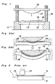
- Fig. 5 illustrates a schematic construction of one prior art apparatus for dividing the wafer.
- the apparatus shown in Fig. 5 comprises a base 1 having a rubber mat 2 placed thereabove.
- a half-cut wafer 3 having first and second surfaces opposite to each other and having chips formed on the first surface thereof is placed on the rubber mat 2 with the first and second surfaces thereof confronting the rubber mat 2 and upwardly, respectively.
- an adhesive tape 15 is applied to the second surface of the wafer so that, when the wafer 3 is divided or separated, the chips will not scatter and can be retained in position.
- the prior art apparatus for dividing the chips formed on the generally circular wafer is so designed that the wafer supported by the rubber mat rich of elasticity placed on the base is divided while the cylindrical rod-like roller is pressed thereagainst. Both of the wafer and the rubber mat when pressed by the cylindrical rod-like roller are downwardly loaded to deform. Because of this, the wafer can be cut only in one direction and, in order for the wafer which has been scribed to be cut in both X-axis and Y-axis directions, a process is required to be repeated two times.
- a peripheral area of the wafer may have a film such as SiN film left unremoved, rendering the peripheral area of the wafer to be thicker than the remainder thereof. Therefore, it occurs that a greater pressing force acts on the peripheral area of the wafer than on a central area thereof.
- DE-A-1908597 discloses an apparatus for separating a wafer into chips, in which the wafer is placed on a flexible mat over a cavity. By means of an applied difference of air pressure across the mat, the wafer is pressed into the cavity to break the wafer along scribed lines into a multiplicity of chips.
- the present invention has been devised with a view to substantially eliminating the above described problems inherent in the prior art apparatus and has for its essential object to provide an improved apparatus for fabricating a semiconductor device which is effective to accurately separate the chips through a single process without the excessive pressing force applied.
- an apparatus for making a semiconductor device comprises a flexible mat, means for supporting the flexible mat in a substantially horizontal position, a pressing means having a generally hemispherical convex body and supported for movement up and down, and a drive means for driving one of the pressing means and supporting means relative to the other of the pressing means and supporting means so as to move up and down.
- the wafer having the first and second surfaces opposite to each other with the chips formed on the first surface thereof is placed on the mat with the chips confronting the flexible mat.
- the convex body of the pressing means is pressed against the second surface of the wafer to separate the chips on the wafer individually.
- the flexible mat may be circular in shape and may be made of rubber.
- the drive means may be adapted to drive the pressing means relative to the wafer.
- the pressing means may be constituted by at least three rods mounted upright on the support means and a pressing plate having the convex body and supported by the three upright rods.
- the convex body may have a surface area substantially larger than the wafer.
- the wafer placed on the flexible mat with the first surface thereof confronting the flexible mat is pressed under a predetermined pressure by the pressing means with the convex body contacting the second surface of the wafer.
- the wafer so pressed deforms to a shape conforming to, and so as to follow, the shape of the convex body of the pressing means whereby cracking of the wafer is initiated from a center thereof, and no higher pressure than the predetermined pressure acts on that portion of the wafer where the cracking has taken place.
- the wafer has the peripheral area having a thickness greater than that of the remainder thereof because of the presence of the film such as SiN film, the cracking of the wafer takes place from the central area thereof with no substantial possibility of the higher pressure acting on the peripheral area of the wafer than that on the central area thereof. Therefore, the chips on the wafer which has been half-cut can be progressively separated from the central area of the wafer in a direction radially outwardly thereof while the predetermined pressure acts uniformly thereon.
- the wafer can be accurately divided into the plurality of chips without damaging the chips and in one process.
- the flexible mat is circular in shape
- both of the mat and the wafer can deform simultaneously with each other so as to follow the curvature of the convex body of the pressing means when the pressing means is applied thereto, and therefore, the pressing force so applied to the wafer is uniform over the whole chips enough to avoid any possible damage to the chips which would occur when the chips are separated.
- the apparatus may further comprise means for supporting a tape, upon which the wafer is to be placed, beneath the mat under tension, and a heating means for heating the convex body of the pressing means.
- the pressing means may comprise a wafer ring surrounding the convex body and supported for movement up and down, and a ring drive means for driving the wafer ring up and down.
- the convex body of the pressing means is preferably heated to about 60°C.
- the convex body heated to a predetermined temperature is pressed against the second surface of the wafer through the tape to separate the chips and, at the same time, the tape is caused to expand to allow the complete separation of the chips.
- the heating of the convex body is advantageous in that the tape is allowed to expand readily to facilitate a ready separation of the chips from the wafer, or a ready breakage of the wafer into the chips.
- the use of the tape support means is particularly advantageous in the following respect.
- the tape is heated to increase the elongation while supported under tension by the tape support means. Therefore, when the pressing means is subsequently pressed against the second surface of the wafer to separate the chips individually, the chips so separated are caused to adhere to the tape.
- the subsequent separation of the pressing means away from the wafer is accompanied by a corresponding movement of the wafer ring so that a tape held taut on the wafer ring can be automatically fitted to the second surface of the wafer thereby to retain the separated chips. In this way, the application of the tape, the separation of the wafer and the expansion of the tape are all performed automatically in the apparatus according to the present invention.
- the pressing means may be positioned either above or beneath the wafer supported by the mat. Where the pressing means is positioned beneath the wafer, the pressing means may be held still while the wafer can be driven by the drive means in a direction close toward or away from the pressing means. Alternatively, where the pressing means is positioned beneath the wafer, the wafer may be held still while the pressing means can be driven by the drive means in a direction close towards and away from the wafer.
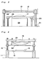
- an apparatus for making a semiconductor device comprises a generally ring-shaped base 11 having a generally circular rubber mat 12 mounted thereon so as to close the opening of the ring-shaped base 11.
- At least three, preferably four, upright posts 15 are rigidly mounted on the base 11 so as to extend upwardly therefrom and spaced an equal distance in a direction circumferentially of the base 11.
- the upright posts 15 carries a generally circular pressing plate 16 mounted thereon so as to lie horizontal, i.e., in a plane perpendicular to any one of the upright posts 15, and so as to move in a direction close towards and away from the rubber mat 12 along the upright posts 15.
- the pressing plate 16 has one surface formed with a generally hemispherical body 17 protruding downwardly towards the rubber mat 12.
- a drive mechanism used to move the pressing plate 16 in a direction close towards and away from the rubber mat 12 along the upright posts 15 is not illustrated, but may be of any known construction.
- a wafer 13 having first and second surfaces opposite to each other with chips formed on the first surface thereof is placed on the rubber mat 12 through a surface protective tape 18 laid between the rubber mat 12 and the wafer 13.
- the second surface of the wafer 13 has a tape 19 applied thereto and, hence, when the wafer 13 is placed on the rubber mat 12 in the manner as hereinabove described, the tape 19 on the second surface of the wafer 12 faces upwards, in a direction opposite to the rubber mat 12.
- the drive mechanism is operated to move the pressing plate 16 downwards in a direction close towards the wafer 13 on the rubber mat 12 along the upright posts 15. Consequent upon the downward movement of the pressing plate 16, the generally hemispherical body 17 on the pressing plate 16 is brought into contact with the wafer 13 through the tape 19 substantially as shown in Fig. 2(a).
- the wafer 13 together with the rubber mat 12 is downwardly deformed, i.e., concaved, by the application of a pressing force thereto from the hemispherical body 17, representing a rounded recess which follows the curvature of the hemispherical body 17 as shown in Fig. 2(b).
- the chips formed on the wafer 13 receive a uniform pressing force transmitted from the hemispherical body 17.
- the application of the pressing force uniformly over the chips on the wafer 13 results not only in the minimization of any possible damage to the chips, but also in the separation of the chips in both of x-axis and y-axis directions perpendicular to each other.
- the apparatus comprises a base 21 having at least three, preferably four, upright posts 25 secured thereto so as to extend upwards, and a generally circular rubber mat 12 mounted thereon through a generally ring-shaped member for movement in a direction close towards and away from the base 21 along the upright posts 25, said rubber mat 12 lying horizontal, i.e., in a plane perpendicular to any one of the upright posts 25.
- the ring-shaped member supporting the rubber mat 12 also supports a tape 28 on which the wafer 13 is placed, said tape 28 being positioned immediately beneath the rubber mat 12.
- the apparatus also comprises a pressing block 26 rigidly mounted on the base 21 and having a generally hemispherical body 17 integrally formed therewith and protruding upwardly so as to confront the wafer 13, and a wafer ring 29 surrounding the hemispherical body 17 and supported on a plurality of support posts for movement up and down in a direction parallel to any one of the support posts.
- the hemispherical body 17 is of a type having a heater embedded therein for heating the hemispherical body 17 to a predetermined temperature, for example, about 60°C.
- the wafer 13 is placed on the tape 28 with the chips on the first surface thereof confronting the rubber mat 12. Thereafter, the drive mechanism (not shown) is operated to move the wafer 13 together with the rubber mat 12 and the tape 28 downwardly in a direction close towards the hemispherical body 17, thereby bringing the wafer 13 into contact with the hemispherical body 17 while the wafer 13 is permitted to deform together with the rubber mat 13 to represent a rounded recess which follows the curvature of the hemispherical body 17.
- the rubber mat 12 is, together with the wafer 13, further moved a predetermined distance downwards to allow the tape 28 to elongate or expand while separating the chips individually. Thereafter, the wafer ring 29 is upwardly shifted by a suitable drive mechanism (not shown) along the support posts to apply a tape 28, which has previously been expanded thereover, to the wafer 13 from below.
- the apparatus shown therein is generally similar to that shown in and described with reference to Fig. 1.
- the apparatus shown in Fig. 4 may be considered a version of the apparatus of Fig. 1 in which a wafer ring 29 corresponding in function to the wafer ring 29 shown in and described with reference to Fig. 3 is provided for automatically applying a tape to the wafer 13.
- the apparatus shown in Fig. 4 is provided not only with the wafer ring 29, but also with a support ring slidably mounted on the upright posts 15 for movement up and down along the upright posts 15, said support ring having a tape 38 stretched thereon so as to lie immediately below the hemispherical body 17.
- Fig. 4 the apparatus shown in Fig. 4 is so designed as to operate in the following manner.
- the wafer 13 having the chips on the first surface thereof is placed on the rubber mat 12 with the chips on held in contact with the rubber mat 12.
- the drive mechanism is operated to move the pressing plate 16 downwards in a direction close towards the wafer 13 on the rubber mat 12 along the upright posts 15.
- the hemispherical body 17 then heated to about 60° is brought into contact with the tape 38 to enhance the ductility of the tape 38.
- the pressing plate 16 is then further moved downwards until the hemispherical body 17 is brought into contact with the wafer 13 on the rubber mat 12.
- the wafer 13 together with the rubber mat 12 is downwardly deformed, i.e., concaved, by the application of a pressing force thereto from the hemispherical body 17, representing a rounded recess which follows the curvature of the hemispherical body 17.
- the wafer ring 29 is lowered to retain the tape 38 pressed against the rubber mat 12.
- the pressing plate 16 in the lowered position is then elevated to leave away from the rubber mat 12, the tape 38 then expanded by the wafer ring 29 is applied to the wafer 12. Thereafter, the wafer ring 29 is upwardly shifted in readiness for the removal of the separated chips then retained in position by the applied tape 38.
Landscapes
- Engineering & Computer Science (AREA)
- Mechanical Engineering (AREA)
- Dicing (AREA)
Claims (8)
- Vorrichtung zum Herstellen eines Halbleiterbauteils mit:
einer flexiblen Matrize (12);
einer Einrichtung (11), um die flexible Matrize (12) in einer im wesentlichen horizontalen Lage zu haltern;
einer Preßeinrichtung (16), die im allgemeinen einen halbkugeligen konvexen Körper (17) aufweist und für eine Aufwärts- und Abwärtsbewegung gehaltert ist; und
einer Antriebseinrichtung, um entweder die Preßeinrichtung (16) relativ zu der flexiblen Matrize (12), oder die flexible Matrize (12) relativ zu der Preßeinrichtung (16) so anzutreiben, um sie in der Weise aufwärts und abwärts zu bewegen, so daß dann, wenn ein Wafer (13) mit ersten und zweiten einander gegenüberliegenden Oberflächen und auf seiner ersten Oberfläche ausgebildeten Chips, der mit den Chips der flexiblen Gummimatrize (12) zugewandt auf der Matrize (12) angeordnet ist, durch den halbkugeligen Körper (17) der Preßeinrichtung (16) über den Kontakt des halbkugeligen Körpers gegen den Mittelpunkt der zweiten Oberfläche des Wafers (13) gepreßt wird, die Chips auf dem Wafer (13) in Einzelstücke getrennt werden, wobei die Trennung vom Mittelpunkt des Wafers aus eingeleitet wird. - Vorrichtung nach Anspruch 1, wobei die flexible Matrize (12) eine runde Form aufweist.
- Vorrichtung nach Anspruch 1 oder 2, wobei die flexible Matrize (12) aus Gummi besteht.
- Vorrichtung nach einem der vorstehenden Ansprüche, wobei die Preßeinrichtung (16) mindestens drei aufrecht stehende Pfosten (15) und eine Preßplatte (16) mit dem halbkugeligen Körper (17) aufweist.
- Vorrichtung nach einem der vorstehenden Ansprüche mit:
einer Einrichtung, um ein Band (28) in horizontaler Richtung unter Spannung unterhalb der flexiblen Matrize (12) und über der Preßeinrichtung (26) zu haltern;
einer Heizeinrichtung zum Aufheizen des halbkugeligen Körpers (17) auf eine vorgegebene Temperatur; und
einer Antriebseinrichtung, um die Matrizenhalteeinrichtung und die Bandhalteeinrichtung relativ zu der Preßeinrichtung (26) in der Art anzutreiben, so daß dann, wenn ein Wafer (13) mit ersten und zweiten einander gegenüberliegenden Oberflächen und auf seiner ersten Oberfläche ausgebildeten Chips, der mit den Chips dem Band (28) zugewandt auf dem Band (28) angeordnet ist, durch den halbkugeligen Körper (17) über das Band gegen die zweite Oberfläche gedrückt wird, die Chips auf dem Wafer (13) in Einzelstücke getrennt werden und das Band (28) zum gleichen Zeitpunkt gedehnt wird, um die Chips vollständig zu trennen. - Vorrichtung nach einem der Ansprüche 1 bis 4 zum Herstellen eines Halbleiterbauteils mit:
einer Einrichtung, um ein Band (38) in horizontaler Richtung unter Spannung über der flexiblen Matrize (12) und unterhalb der Preßeinrichtung (16) zu haltern;
einer Heizeinrichtung zum Aufheizen des halbkugeligen konvexen Körpers (17) auf eine vorgegebene Temperatur; und
einer Antriebseinrichtung, um die Matrizenhalteeinrichtung und die Bandhalteeinrichtung relativ zu der Preßeinrichtung (16) in der Art anzutreiben, so daß dann, wenn ein Wafer (13) mit ersten und zweiten einander gegenüberliegenden Oberflächen und auf seiner ersten Oberfläche ausgebildeten Chips, der mit den Chips der flexiblen Matrize (12) zugewandt auf der Matrize (12) angeordnet ist, durch den halbkugeligen konvexen Körper der Preßeinrichtung über das Band gepreßt wird, die Chips auf dem Wafer in Einzelstücke getrennt werden und das Band (38) zum gleichen Zeitpunkt gedehnt wird, um die Chips vollständig zu trennen. - Vorrichtung nach Anspruch 5 oder 6, wobei die vorgegebene Temperatur etwa 60°C ist.
- Vorrichtung nach einem der vorstehenden Ansprüche, welche ferner einen für eine Aufwärts- und Abwärtsbewegung gehalterten Waferring (29) und eine Ringantriebseinrichtung für den Antrieb des Waferrings (29) aufweist.
Applications Claiming Priority (6)
| Application Number | Priority Date | Filing Date | Title |
|---|---|---|---|
| JP10811987A JP2567396B2 (ja) | 1987-05-01 | 1987-05-01 | 半導体素子製造装置 |
| JP108119/87 | 1987-05-01 | ||
| JP10811887A JP2567395B2 (ja) | 1987-05-01 | 1987-05-01 | 半導体素子製造装置 |
| JP62108117A JPS63272509A (ja) | 1987-05-01 | 1987-05-01 | 半導体素子製造装置 |
| JP108118/87 | 1987-05-01 | ||
| JP108117/87 | 1987-05-01 |
Publications (3)
| Publication Number | Publication Date |
|---|---|
| EP0289045A2 EP0289045A2 (de) | 1988-11-02 |
| EP0289045A3 EP0289045A3 (de) | 1991-01-16 |
| EP0289045B1 true EP0289045B1 (de) | 1994-07-06 |
Family
ID=27311150
Family Applications (1)
| Application Number | Title | Priority Date | Filing Date |
|---|---|---|---|
| EP19880106915 Expired - Lifetime EP0289045B1 (de) | 1987-05-01 | 1988-04-29 | Vorrichtung zur Herstellung von Halbleiter-Bauelementen |
Country Status (5)
| Country | Link |
|---|---|
| US (1) | US5104023A (de) |
| EP (1) | EP0289045B1 (de) |
| KR (1) | KR920004514B1 (de) |
| CA (1) | CA1311314C (de) |
| DE (1) | DE3850519T2 (de) |
Families Citing this family (14)
| Publication number | Priority date | Publication date | Assignee | Title |
|---|---|---|---|---|
| DE4006070A1 (de) * | 1990-02-27 | 1991-09-12 | Braun Ag | Verfahren und einrichtung zum zerteilen einer scheibe aus halbleitermaterial |
| JP3552772B2 (ja) * | 1994-01-21 | 2004-08-11 | アマダ・エムエフジー・アメリカ・インコーポレイティド | ミクロジョイント加工用製品分離方法 |
| JP3409928B2 (ja) * | 1994-10-15 | 2003-05-26 | 株式会社東芝 | 半導体装置の製造方法 |
| US5543365A (en) * | 1994-12-02 | 1996-08-06 | Texas Instruments Incorporated | Wafer scribe technique using laser by forming polysilicon |
| US5710065A (en) * | 1995-01-03 | 1998-01-20 | Texas Instruments Incorporated | Method and apparatus for breaking and separating dies from a wafer |
| US6685073B1 (en) | 1996-11-26 | 2004-02-03 | Texas Instruments Incorporated | Method and apparatus for stretching and processing saw film tape after breaking a partially sawn wafer |
| US6184063B1 (en) | 1996-11-26 | 2001-02-06 | Texas Instruments Incorporated | Method and apparatus for breaking and separating a wafer into die using a multi-radii dome |
| JP4322328B2 (ja) * | 1997-06-05 | 2009-08-26 | テキサス インスツルメンツ インコーポレイテツド | ウエハをウエハテープに接着する方法および装置 |
| US5913468A (en) * | 1998-01-06 | 1999-06-22 | Amada Engineering & Service, Inc. | Micro-joint part separator |
| US6098862A (en) * | 1998-05-18 | 2000-08-08 | Lucent Technologies Inc. | Incrementally continuous laser cleaving process |
| US6205994B1 (en) * | 1998-12-23 | 2001-03-27 | Lucent Technologies, Inc. | Scriber adapter plate |
| US6541352B2 (en) | 2001-07-27 | 2003-04-01 | Texas Instruments Incorporated | Semiconductor die with contoured bottom surface and method for making same |
| US6686225B2 (en) | 2001-07-27 | 2004-02-03 | Texas Instruments Incorporated | Method of separating semiconductor dies from a wafer |
| US20180323105A1 (en) * | 2017-05-02 | 2018-11-08 | Psemi Corporation | Simultaneous Break and Expansion System for Integrated Circuit Wafers |
Family Cites Families (11)
| Publication number | Priority date | Publication date | Assignee | Title |
|---|---|---|---|---|
| FR1481711A (fr) * | 1965-06-02 | 1967-05-19 | Nippon Electric Co | Dispositif pour briser une masse semi-conductrice en morceaux élémentaires |
| US3562057A (en) * | 1967-05-16 | 1971-02-09 | Texas Instruments Inc | Method for separating substrates |
| US3507426A (en) * | 1968-02-23 | 1970-04-21 | Rca Corp | Method of dicing semiconductor wafers |
| US3493155A (en) * | 1969-05-05 | 1970-02-03 | Nasa | Apparatus and method for separating a semiconductor wafer |
| US3727282A (en) * | 1970-02-05 | 1973-04-17 | Burroughs Corp | Semiconductor handling apparatus |
| US3743148A (en) * | 1971-03-08 | 1973-07-03 | H Carlson | Wafer breaker |
| US3790051A (en) * | 1971-09-07 | 1974-02-05 | Radiant Energy Systems | Semiconductor wafer fracturing technique employing a pressure controlled roller |
| US3918150A (en) * | 1974-02-08 | 1975-11-11 | Gen Electric | System for separating a semiconductor wafer into discrete pellets |
| US4247031A (en) * | 1979-04-10 | 1981-01-27 | Rca Corporation | Method for cracking and separating pellets formed on a wafer |
| US4410168A (en) * | 1980-07-11 | 1983-10-18 | Asta, Ltd. | Apparatus for manipulating a stretched resilient diaphragm |
| FR2516848A1 (fr) * | 1981-11-25 | 1983-05-27 | Radiotechnique Compelec | Procede et machine pour subdiviser une plaque de ceramiquea |
-
1988
- 1988-04-27 KR KR1019880004778A patent/KR920004514B1/ko not_active Expired
- 1988-04-29 EP EP19880106915 patent/EP0289045B1/de not_active Expired - Lifetime
- 1988-04-29 CA CA 565564 patent/CA1311314C/en not_active Expired - Lifetime
- 1988-04-29 DE DE3850519T patent/DE3850519T2/de not_active Expired - Fee Related
-
1991
- 1991-04-08 US US07/681,670 patent/US5104023A/en not_active Expired - Fee Related
Also Published As
| Publication number | Publication date |
|---|---|
| US5104023A (en) | 1992-04-14 |
| DE3850519D1 (de) | 1994-08-11 |
| DE3850519T2 (de) | 1994-12-01 |
| KR920004514B1 (ko) | 1992-06-08 |
| EP0289045A2 (de) | 1988-11-02 |
| EP0289045A3 (de) | 1991-01-16 |
| CA1311314C (en) | 1992-12-08 |
| KR880014643A (ko) | 1988-12-24 |
Similar Documents
| Publication | Publication Date | Title |
|---|---|---|
| EP0289045B1 (de) | Vorrichtung zur Herstellung von Halbleiter-Bauelementen | |
| KR101151023B1 (ko) | 익스팬드방법 및 익스팬드장치 | |
| KR101109256B1 (ko) | 반도체 웨이퍼의 소편화 방법 및 이를 이용한 장치 | |
| US10559487B2 (en) | Wafer dividing method and dividing apparatus | |
| US20070277929A1 (en) | Method and Device for Detaching a Component Which is Attached to a Flexible Film | |
| JP2005117019A (ja) | 半導体装置の製造方法 | |
| JP2006049591A (ja) | ウエーハに貼着された接着フィルムの破断方法および破断装置 | |
| US5303861A (en) | Separating sheet glass | |
| JP2004304066A (ja) | 半導体装置の製造方法 | |
| JPH05259276A (ja) | 半導体ウェーハへのテープ添着方法とその装置 | |
| US5288663A (en) | Method for extending wafer-supporting sheet | |
| JP2004193241A (ja) | 半導体ウエーハの分割方法 | |
| US6007654A (en) | Noncontact method of adhering a wafer to a wafer tape | |
| JP2007027250A (ja) | ウエーハに装着された接着フィルムの破断装置 | |
| US4775085A (en) | Semiconductor wafer breaking apparatus | |
| JPH0541451A (ja) | 半導体ウエハのペレタイズ方法と装置 | |
| JP5345348B2 (ja) | 破断方法及び破断装置 | |
| JP2567395B2 (ja) | 半導体素子製造装置 | |
| JPH07321070A (ja) | ウェハのエキスパンド方法 | |
| JP2567396B2 (ja) | 半導体素子製造装置 | |
| JPS59130438A (ja) | 板状物の分離法 | |
| JP2011086866A (ja) | 半導体デバイスの製造方法 | |
| JPH07122583A (ja) | 半導体装置の製造方法及び半導体製造装置 | |
| CN110148572B (zh) | 分割装置 | |
| JP2003068832A (ja) | ダイシングテープおよびその使用方法 |
Legal Events
| Date | Code | Title | Description |
|---|---|---|---|
| PUAI | Public reference made under article 153(3) epc to a published international application that has entered the european phase |
Free format text: ORIGINAL CODE: 0009012 |
|
| AK | Designated contracting states |
Kind code of ref document: A2 Designated state(s): DE FR GB IT |
|
| PUAL | Search report despatched |
Free format text: ORIGINAL CODE: 0009013 |
|
| AK | Designated contracting states |
Kind code of ref document: A3 Designated state(s): DE FR GB IT |
|
| 17P | Request for examination filed |
Effective date: 19901220 |
|
| 17Q | First examination report despatched |
Effective date: 19920611 |
|
| GRAA | (expected) grant |
Free format text: ORIGINAL CODE: 0009210 |
|
| AK | Designated contracting states |
Kind code of ref document: B1 Designated state(s): DE FR GB IT |
|
| REF | Corresponds to: |
Ref document number: 3850519 Country of ref document: DE Date of ref document: 19940811 |
|
| ITF | It: translation for a ep patent filed | ||
| ET | Fr: translation filed | ||
| PLBE | No opposition filed within time limit |
Free format text: ORIGINAL CODE: 0009261 |
|
| STAA | Information on the status of an ep patent application or granted ep patent |
Free format text: STATUS: NO OPPOSITION FILED WITHIN TIME LIMIT |
|
| 26N | No opposition filed | ||
| PGFP | Annual fee paid to national office [announced via postgrant information from national office to epo] |
Ref country code: FR Payment date: 19960410 Year of fee payment: 9 |
|
| PGFP | Annual fee paid to national office [announced via postgrant information from national office to epo] |
Ref country code: GB Payment date: 19960422 Year of fee payment: 9 |
|
| PGFP | Annual fee paid to national office [announced via postgrant information from national office to epo] |
Ref country code: DE Payment date: 19960429 Year of fee payment: 9 |
|
| PG25 | Lapsed in a contracting state [announced via postgrant information from national office to epo] |
Ref country code: GB Effective date: 19970429 |
|
| GBPC | Gb: european patent ceased through non-payment of renewal fee |
Effective date: 19970429 |
|
| PG25 | Lapsed in a contracting state [announced via postgrant information from national office to epo] |
Ref country code: FR Free format text: LAPSE BECAUSE OF NON-PAYMENT OF DUE FEES Effective date: 19971231 |
|
| PG25 | Lapsed in a contracting state [announced via postgrant information from national office to epo] |
Ref country code: DE Free format text: LAPSE BECAUSE OF NON-PAYMENT OF DUE FEES Effective date: 19980101 |
|
| REG | Reference to a national code |
Ref country code: FR Ref legal event code: ST |
|
| PG25 | Lapsed in a contracting state [announced via postgrant information from national office to epo] |
Ref country code: IT Free format text: LAPSE BECAUSE OF NON-PAYMENT OF DUE FEES;WARNING: LAPSES OF ITALIAN PATENTS WITH EFFECTIVE DATE BEFORE 2007 MAY HAVE OCCURRED AT ANY TIME BEFORE 2007. THE CORRECT EFFECTIVE DATE MAY BE DIFFERENT FROM THE ONE RECORDED. Effective date: 20050429 |