EP0285440A2 - Diffundierte Widerstandsschaltung - Google Patents
Diffundierte Widerstandsschaltung Download PDFInfo
- Publication number
- EP0285440A2 EP0285440A2 EP88302945A EP88302945A EP0285440A2 EP 0285440 A2 EP0285440 A2 EP 0285440A2 EP 88302945 A EP88302945 A EP 88302945A EP 88302945 A EP88302945 A EP 88302945A EP 0285440 A2 EP0285440 A2 EP 0285440A2
- Authority
- EP
- European Patent Office
- Prior art keywords
- resistor
- area
- diffusion
- circuit
- island
- Prior art date
- Legal status (The legal status is an assumption and is not a legal conclusion. Google has not performed a legal analysis and makes no representation as to the accuracy of the status listed.)
- Ceased
Links
- 238000009792 diffusion process Methods 0.000 title claims abstract description 84
- 239000000758 substrate Substances 0.000 claims abstract description 15
- 239000012535 impurity Substances 0.000 claims abstract description 9
- 230000008878 coupling Effects 0.000 claims description 10
- 238000010168 coupling process Methods 0.000 claims description 10
- 238000005859 coupling reaction Methods 0.000 claims description 10
- 238000004458 analytical method Methods 0.000 description 9
- 230000004048 modification Effects 0.000 description 5
- 238000012986 modification Methods 0.000 description 5
- 229910021420 polycrystalline silicon Inorganic materials 0.000 description 5
- 230000008859 change Effects 0.000 description 4
- 230000009471 action Effects 0.000 description 2
- 238000002955 isolation Methods 0.000 description 2
- 238000004519 manufacturing process Methods 0.000 description 2
- 238000004891 communication Methods 0.000 description 1
- 230000003247 decreasing effect Effects 0.000 description 1
- 230000000694 effects Effects 0.000 description 1
- 239000000463 material Substances 0.000 description 1
- 238000000034 method Methods 0.000 description 1
- 230000008569 process Effects 0.000 description 1
- 230000009467 reduction Effects 0.000 description 1
- 230000004044 response Effects 0.000 description 1
- 239000004065 semiconductor Substances 0.000 description 1
- 230000007480 spreading Effects 0.000 description 1
- 230000001629 suppression Effects 0.000 description 1
Images


Classifications
-
- H—ELECTRICITY
- H10—SEMICONDUCTOR DEVICES; ELECTRIC SOLID-STATE DEVICES NOT OTHERWISE PROVIDED FOR
- H10D—INORGANIC ELECTRIC SEMICONDUCTOR DEVICES
- H10D84/00—Integrated devices formed in or on semiconductor substrates that comprise only semiconducting layers, e.g. on Si wafers or on GaAs-on-Si wafers
- H10D84/201—Integrated devices formed in or on semiconductor substrates that comprise only semiconducting layers, e.g. on Si wafers or on GaAs-on-Si wafers characterised by the integration of only components covered by H10D1/00 or H10D8/00, e.g. RLC circuits
- H10D84/204—Integrated devices formed in or on semiconductor substrates that comprise only semiconducting layers, e.g. on Si wafers or on GaAs-on-Si wafers characterised by the integration of only components covered by H10D1/00 or H10D8/00, e.g. RLC circuits of combinations of diodes or capacitors or resistors
- H10D84/209—Integrated devices formed in or on semiconductor substrates that comprise only semiconducting layers, e.g. on Si wafers or on GaAs-on-Si wafers characterised by the integration of only components covered by H10D1/00 or H10D8/00, e.g. RLC circuits of combinations of diodes or capacitors or resistors of only resistors
-
- H—ELECTRICITY
- H10—SEMICONDUCTOR DEVICES; ELECTRIC SOLID-STATE DEVICES NOT OTHERWISE PROVIDED FOR
- H10D—INORGANIC ELECTRIC SEMICONDUCTOR DEVICES
- H10D84/00—Integrated devices formed in or on semiconductor substrates that comprise only semiconducting layers, e.g. on Si wafers or on GaAs-on-Si wafers
- H10D84/80—Integrated devices formed in or on semiconductor substrates that comprise only semiconducting layers, e.g. on Si wafers or on GaAs-on-Si wafers characterised by the integration of at least one component covered by groups H10D12/00 or H10D30/00, e.g. integration of IGFETs
- H10D84/811—Combinations of field-effect devices and one or more diodes, capacitors or resistors
Definitions
- the present invention relates generally to a diffusion resistor circuit, and more particularly to a circuit arrangement of diffusion resistors suitable for a bipolar integrated circuit apparatus.
- Bipolar integrated circuits for example, bipolar analog integrated circuits comprise a large number of resistors.
- the resistors of the bipolar integrated circuits typically are made by diffusion processes.
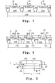
- FIGURE 1 A typical diffusion resistor is shown in FIGURE 1.
- the diffusion resistors 10 are comprised of the island areas 10a diffused in a substrate 10b and resistor areas 10c diffused in the island areas 10a.
- the diffusion resistors 10 are separated from other diffusion resistors 10 or other circuit elements by isolation areas 10d diffused between the island areas 10a.
- the island area 10a and the resistor area 10c correspond to the collector area and the base area of typical transistors constructed on the integrated circuit by diffusion processes.
- the diffusion resistors 10 are connected in series by coupling the resistor areas to the adjacent resistor areas.
- Bipolar analog integrated circuits for audio apparatus are required to have less distortion.
- diffusion resistors are insufficient in respect to distortion, compared to other types of resistors. Therefore, some proposals have been made for reducing distortion of circuits having diffusion resistors.
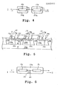
- FIGURE 2 of this application An equivalent circuit to that of the above article is shown in FIGURE 2 of this application for convenience' sake.
- three diffusion resistors 10 are connected in series.
- one end terminal 10e of each resistor area 10c is coupled to an island area 10a thereof.
- the potential of the one end terminal 10e of the resistor area 10c is equalized to the potential of the island area 10a in each diffusion resistor 10.
- the diffusion resistors 10 are coupled in series to obtain a desired value of resistance.
- the island areas 10a coupled to the one end terminals 10e of the resistor areas 10c are coupled to the other end terminals 10f of adjacent diffusion resistors 10. Therefore, the potentials of the island areas 10a are applied to the same end terminals 10e of the resistor areas 10c.
- the article says that the diffusion resistor circuit reduces distortion lower than the distortion in prior circuits by one order. However, the reduction of the distortion is still insufficient for higher grade audio apparatus. This is because the distortion generated by the resistor areas 10d is accumulated in the series circuit.
- Fig. 14 in this Report shows a graph of total distortion to output voltage response characteristics.
- the total distortion in the case of the poly-silicon resistor is reduced greatly in comparison to distortion in the case of diffusion resistors.
- the report is limited to an application for an inverse phase feedback amplifier, as shown in Fig. 13, on page 59 of the report. That is, the poly-silicon resistor itself has a typical resistance value like diffusion resistors. Further, the poly-silicon resistor has some drawbacks in that it requires many steps to manufacture and is high in cost compared to other diffusion resistors.
- the present invention seeks to provide a diffusion resistor circuit which has a reduced distortion.
- the present invention also seeks to provide a diffusion resistor circuit which can be made without the need for special processes in manufacturing.
- the present invention seeks to provide a diffusion resistor circuit which can be manufactured at a low cost.
- a diffusion resistor circuit comprises a diffusion resistor including a substrate, an island area including an impurity of a first polarity diffused into the substrate, a resistor are a including an impurity of a second polarity diffused into the island area and a first circuit coupling for supplying a current signal through the resistor area, characterised in that the diffusion resistor circuit further comprises a second circuit coupling connecting the island area to a generally central point of the resistor area.
- a diffusion resistor circuit comprises a plurality of diffusion resistors, each including a substrate, an island area including an impurity of a first polarity diffused into the substrate, a resistor area including a plurality of a second polarity diffused into the island area and input terminal and an output terminal, a first circuit coupling connecting the resistor areas of the plurality of diffusion resistors in series for supplying a current signal through the resistor areas and a second circuit coupling alternately connecting the island area of each successive adjacent pair of diffusion resistors to the input terminal of one resistor area and the output terminal of the adjacent resistor area.
- FIGURES 5 through 9 the same reference numerals or letters used in FIGURES 1, 2, 3 and 4 (Prior Art ) will be used to designate like or equivalent elements for simplicity of explanation.
- FIGURE 5 a first embodiment of the diffusion resistor circuit according to the present invention will be described in detail.
- FIGURE 5 a substrate (P-type semiconductor) 10b, island areas 10a (N ⁇ channel) diffused into the substrate 10b, isolation areas (P+ channel) 10d isolating the island areas 10a from other island areas 10a or other circuit elements on the substrate 10b, and resistor areas (P channel) 10a diffused into the island areas 10a are indicated.
- the diffusion resistors 10 are formed by diffusion in the substrate 10b.
- each resistor area 10c of the diffusion resistor 10 one terminal 10e and another terminal 10f are respectively located at one end with another end of the resistor area 10c.
- the one terminal 10e of the one resistor area 10c is coupled to the other terminal 10f of the resistor area 10c of the adjacent diffusion resistor 10.
- Center terminals 10g are also located at the center of the resistor area 10c.
- the center terminals 10g are coupled to the island areas 10a.
- Distortion generated by diffusion resistors can be explained as the spreading of depletion layers due to the bias voltage between resistor areas 10c and the island areas 10a. It is known that a change in resistance is in proportion to the square root of the approximate value of the bias voltage. A change in resistance can be theoretically analyzed as described below.
- a change in diffusion resistance is given by; wherein ⁇ is junction potential, Vs is inverse bias voltage (applied externally), and ⁇ is a coefficient.
- Vs ⁇ F ⁇ I (4)
- W is the width of the resistor area 10c
- l is the distance of the measuring point from the reference position, i.e., the other end 10f of the resistor area 10c
- ⁇ F is the sheet resistance at zero bias.
- the total resistance R(I) given by the modulation of the depletion layer is defined as follows:
- the diffusion resistor circuit according to the present invention can be analyzed by using FIGURE 6.
- the tertiary distortion THD3 ⁇ is the same as the tertiary distortion THD3 in the embodiment of FIGURE 6.
- FIGURE 3 typically diffusion resistor
- FIGURE 4 NIKKEI ELECTRONICS
- FIGURE 5 present invention
- the secondary distortion THD2 ⁇ is theoretically removed, leaving only the tertiary distortion THD3 ⁇ .
- the total distortion of the present invention becomes smaller. This is because the central point of the resistor area 10c is connected to the island area 10a. Then, the distortions generated by the left and right part resistors Rl and Rr of the resistor 10c will have opposite phase to each other. Thus, they give a push-pull action to cancel the distortions mutually, as shown in FIGURE 7.
- FIGURE 8 shows a second embodiment according to the present invention.
- This second embodiment reveals that it is possible to obtain the same effect as the above-mentioned first embodiment by alternately selecting the terminal on the input side and the terminal on the output side of each adjacent diffusion resistor 10 connected in series and by connecting each terminal selected to the adjacent diffusion resistor island area 10a. That is to say, according to the second embodiment, if the two diffusion resistors 10 are considered to be one pair, this pair will work as one diffusion resistor 10 in the same way as one diffusion resistor 10 in FIGURE 5.
- FIGURE 9 shows a modification of the first embodiment according to the present invention.
- a circuit connection is carried out by using a level shift circuits 20 so that the potential of the each island area 10a can be shifted from the potential of the central point 10g of the resistor area 10c by a specified voltage.
- the push-pull action of distortion can be obtained with an inverse voltage kept high between the resistor area 10c and the island area 10a, decreasing the generation of distortion.
- the present invention enables distortion owing to the depletion layer to be lower than the distortion of the prior circuit by one order of magnitude.
- the invention uses diffusion resistors which generate lower noise than poly- silicon resistors. Being produced easily, the diffusion resistor enables the present invention to be embodied at small cost.
Landscapes
- Semiconductor Integrated Circuits (AREA)
- Amplifiers (AREA)
Applications Claiming Priority (2)
| Application Number | Priority Date | Filing Date | Title |
|---|---|---|---|
| JP78580/87 | 1987-03-31 | ||
| JP62078580A JPS63244765A (ja) | 1987-03-31 | 1987-03-31 | 拡散抵抗を有する集積回路 |
Publications (2)
| Publication Number | Publication Date |
|---|---|
| EP0285440A2 true EP0285440A2 (de) | 1988-10-05 |
| EP0285440A3 EP0285440A3 (de) | 1990-12-12 |
Family
ID=13665844
Family Applications (1)
| Application Number | Title | Priority Date | Filing Date |
|---|---|---|---|
| EP19880302945 Ceased EP0285440A3 (de) | 1987-03-31 | 1988-03-31 | Diffundierte Widerstandsschaltung |
Country Status (4)
| Country | Link |
|---|---|
| US (1) | US5111068A (de) |
| EP (1) | EP0285440A3 (de) |
| JP (1) | JPS63244765A (de) |
| KR (1) | KR910008987B1 (de) |
Cited By (1)
| Publication number | Priority date | Publication date | Assignee | Title |
|---|---|---|---|---|
| EP0472331A3 (en) * | 1990-08-20 | 1993-04-21 | Hughes Aircraft Company | Integrated circuit resistor fabrication using focused ion beam |
Families Citing this family (15)
| Publication number | Priority date | Publication date | Assignee | Title |
|---|---|---|---|---|
| JPH0423355A (ja) * | 1990-05-15 | 1992-01-27 | Hitachi Ltd | 半導体装置 |
| FR2689316B1 (fr) * | 1992-03-25 | 1994-06-17 | Dolphin Integration Sa | Pont diviseur auto-protege. |
| US5428297A (en) * | 1993-06-15 | 1995-06-27 | Grace; James W. | Precision integrated resistors |
| JPH07211510A (ja) * | 1994-01-27 | 1995-08-11 | Nippondenso Co Ltd | 半導体装置 |
| JP3344138B2 (ja) * | 1995-01-30 | 2002-11-11 | 株式会社日立製作所 | 半導体複合センサ |
| US5739577A (en) * | 1995-04-21 | 1998-04-14 | Micron Technology, Inc. | Resistive structure for integrated circuits and method of forming same |
| CA2179246C (en) * | 1995-09-20 | 2000-10-24 | Pmc-Sierra Ltd. | Polysilicon defined diffused resistor |
| IT1311280B1 (it) * | 1999-12-24 | 2002-03-12 | St Microelectronics Srl | Struttura di resistore integrato verticale di ingombro ridotto peralta tensione e relativo processo di fabbricazione. |
| DE10243604B4 (de) * | 2002-09-19 | 2006-07-27 | Infineon Technologies Ag | Anordnung von mehreren Widerständen eines Halbleiter-Bauelements |
| US8384157B2 (en) * | 2006-05-10 | 2013-02-26 | International Rectifier Corporation | High ohmic integrated resistor with improved linearity |
| JP5315604B2 (ja) * | 2006-09-29 | 2013-10-16 | 富士通セミコンダクター株式会社 | 半導体集積回路 |
| US7902907B2 (en) * | 2007-12-12 | 2011-03-08 | Micron Technology, Inc. | Compensation capacitor network for divided diffused resistors for a voltage divider |
| JP2010109233A (ja) * | 2008-10-31 | 2010-05-13 | Renesas Technology Corp | 半導体装置 |
| CN102569299A (zh) * | 2010-12-14 | 2012-07-11 | 无锡华润矽科微电子有限公司 | 耗尽型mos管电阻器及其形成方法 |
| JP5828877B2 (ja) * | 2013-12-09 | 2015-12-09 | ウィンボンド エレクトロニクス コーポレーション | 半導体装置 |
Family Cites Families (10)
| Publication number | Priority date | Publication date | Assignee | Title |
|---|---|---|---|---|
| US4141023A (en) * | 1973-08-11 | 1979-02-20 | Sony Corporation | Field effect transistor having a linear attenuation characteristic and an improved distortion factor with multiple gate drain contacts |
| US3990092A (en) * | 1974-01-11 | 1976-11-02 | Hitachi, Ltd. | Resistance element for semiconductor integrated circuit |
| FR2351505A1 (fr) * | 1976-05-13 | 1977-12-09 | Ibm France | Procede de correction du coefficient en tension de resistances semi-conductrices, implantees ou diffusees |
| US4034395A (en) * | 1976-09-29 | 1977-07-05 | Honeywell Inc. | Monolithic integrated circuit having a plurality of resistor regions electrically connected in series |
| US4044371A (en) * | 1976-09-29 | 1977-08-23 | Honeywell Inc. | Plurality of precise temperature resistors formed in monolithic integrated circuits |
| US4164668A (en) * | 1977-05-12 | 1979-08-14 | International Business Machines Corporation | Method of correcting the voltage coefficient of resistors implanted or diffused in a semiconductor substrate |
| FR2430092A1 (fr) * | 1978-06-29 | 1980-01-25 | Ibm France | Procede de correction du coefficient en tension de resistances semi-conductrices, diffusees ou implantees et resistances ainsi obtenues |
| DE3009042A1 (de) * | 1979-03-19 | 1980-10-02 | Trw Inc | Halbleiterwiderstand |
| JPS593963A (ja) * | 1982-06-30 | 1984-01-10 | Fujitsu Ltd | 半導体集積回路 |
| JPS6035555A (ja) * | 1984-05-30 | 1985-02-23 | Nec Corp | 半導体集積回路装置 |
-
1987
- 1987-03-31 JP JP62078580A patent/JPS63244765A/ja active Pending
-
1988
- 1988-03-30 KR KR1019880003508A patent/KR910008987B1/ko not_active Expired
- 1988-03-30 US US07/175,294 patent/US5111068A/en not_active Expired - Fee Related
- 1988-03-31 EP EP19880302945 patent/EP0285440A3/de not_active Ceased
Cited By (1)
| Publication number | Priority date | Publication date | Assignee | Title |
|---|---|---|---|---|
| EP0472331A3 (en) * | 1990-08-20 | 1993-04-21 | Hughes Aircraft Company | Integrated circuit resistor fabrication using focused ion beam |
Also Published As
| Publication number | Publication date |
|---|---|
| KR910008987B1 (ko) | 1991-10-26 |
| EP0285440A3 (de) | 1990-12-12 |
| US5111068A (en) | 1992-05-05 |
| KR880011922A (ko) | 1988-10-31 |
| JPS63244765A (ja) | 1988-10-12 |
Similar Documents
| Publication | Publication Date | Title |
|---|---|---|
| EP0285440A2 (de) | Diffundierte Widerstandsschaltung | |
| EP0442492B1 (de) | Aktiver Filter | |
| US3477031A (en) | Differential amplifier circuit employing multiple differential amplifier stages | |
| DE69617369T2 (de) | Verstärkerschaltung mit variabler Verstärkung | |
| US6642741B2 (en) | Electronically adjustable integrated circuit input/output termination method and apparatus | |
| US4994774A (en) | Integrated low-pass filter arrangement | |
| KR0148324B1 (ko) | 가변 이득 증폭 회로 | |
| US4283641A (en) | Feedback biasing circuit arrangement for transistor amplifier | |
| US4376251A (en) | Waveform shaping circuit | |
| US5416357A (en) | Semiconductor integrated circuit device | |
| US3742377A (en) | Differential amplifier with means for balancing out offset terms | |
| DE68915221T2 (de) | Verstärker. | |
| US4612521A (en) | Charge-coupled transversal filter | |
| GB2295288A (en) | Wideband constant impedance amplifiers | |
| US5130529A (en) | Semiconductor optical position sensing device | |
| DE69219687T2 (de) | Optoelektronische integrierte Schaltung | |
| EP0589676A1 (de) | Variable Spannung-Strom-Wandlerschaltung | |
| US4812734A (en) | Current-mirror arrangement | |
| JPS6057727B2 (ja) | ミユ−テイング回路 | |
| EP0760165B1 (de) | Elektronische anordnung mit mitteln zum kompensieren von parasitären kapazitäten | |
| EP0406865A2 (de) | Demodulationsschaltung | |
| JPS5952847B2 (ja) | 可変インピ−ダンス回路 | |
| US6867636B2 (en) | Circuit arrangement for a current-controlled resistor having an enlarged linear range | |
| EP0091996B1 (de) | Elektrische Schaltung zur Ermittlung des Maxmimalwertes einer Mehrzahl von Eingangströmen und Signalverarbeitungsanordnung, in der eine solche Schaltung verwendet ist. | |
| DE2756777B2 (de) | Digitalschaltungselement |
Legal Events
| Date | Code | Title | Description |
|---|---|---|---|
| PUAI | Public reference made under article 153(3) epc to a published international application that has entered the european phase |
Free format text: ORIGINAL CODE: 0009012 |
|
| 17P | Request for examination filed |
Effective date: 19880419 |
|
| AK | Designated contracting states |
Kind code of ref document: A2 Designated state(s): DE FR GB |
|
| PUAL | Search report despatched |
Free format text: ORIGINAL CODE: 0009013 |
|
| AK | Designated contracting states |
Kind code of ref document: A3 Designated state(s): DE FR GB |
|
| 17Q | First examination report despatched |
Effective date: 19921130 |
|
| STAA | Information on the status of an ep patent application or granted ep patent |
Free format text: STATUS: THE APPLICATION HAS BEEN REFUSED |
|
| 18R | Application refused |
Effective date: 19960122 |