EP0283066A1 - Integrierte Struktur für ein Signalübertragungsnetzwerk, insbesondere für einen Pilotschaltkreis für MOS-Leistungstransistoren - Google Patents
Integrierte Struktur für ein Signalübertragungsnetzwerk, insbesondere für einen Pilotschaltkreis für MOS-Leistungstransistoren Download PDFInfo
- Publication number
- EP0283066A1 EP0283066A1 EP88200290A EP88200290A EP0283066A1 EP 0283066 A1 EP0283066 A1 EP 0283066A1 EP 88200290 A EP88200290 A EP 88200290A EP 88200290 A EP88200290 A EP 88200290A EP 0283066 A1 EP0283066 A1 EP 0283066A1
- Authority
- EP
- European Patent Office
- Prior art keywords
- doping
- type
- integrated structure
- accordance
- components
- Prior art date
- Legal status (The legal status is an assumption and is not a legal conclusion. Google has not performed a legal analysis and makes no representation as to the accuracy of the status listed.)
- Ceased
Links
- 239000000758 substrate Substances 0.000 claims abstract description 15
- 238000009413 insulation Methods 0.000 claims abstract description 6
- 239000004065 semiconductor Substances 0.000 claims abstract description 6
- 238000009792 diffusion process Methods 0.000 claims abstract description 4
- 238000001465 metallisation Methods 0.000 claims description 2
- 239000004020 conductor Substances 0.000 claims 2
- 230000008878 coupling Effects 0.000 description 3
- 238000010168 coupling process Methods 0.000 description 3
- 238000005859 coupling reaction Methods 0.000 description 3
- 238000010586 diagram Methods 0.000 description 2
- 230000010354 integration Effects 0.000 description 2
- 238000000034 method Methods 0.000 description 2
- 244000045947 parasite Species 0.000 description 2
- 230000000295 complement effect Effects 0.000 description 1
- 230000008030 elimination Effects 0.000 description 1
- 238000003379 elimination reaction Methods 0.000 description 1
- 229910021420 polycrystalline silicon Inorganic materials 0.000 description 1
- 229920005591 polysilicon Polymers 0.000 description 1
Images


Classifications
-
- H—ELECTRICITY
- H10—SEMICONDUCTOR DEVICES; ELECTRIC SOLID-STATE DEVICES NOT OTHERWISE PROVIDED FOR
- H10D—INORGANIC ELECTRIC SEMICONDUCTOR DEVICES
- H10D84/00—Integrated devices formed in or on semiconductor substrates that comprise only semiconducting layers, e.g. on Si wafers or on GaAs-on-Si wafers
- H10D84/40—Integrated devices formed in or on semiconductor substrates that comprise only semiconducting layers, e.g. on Si wafers or on GaAs-on-Si wafers characterised by the integration of at least one component covered by groups H10D12/00 or H10D30/00 with at least one component covered by groups H10D10/00 or H10D18/00, e.g. integration of IGFETs with BJTs
- H10D84/401—Combinations of FETs or IGBTs with BJTs
-
- H—ELECTRICITY
- H01—ELECTRIC ELEMENTS
- H01L—SEMICONDUCTOR DEVICES NOT COVERED BY CLASS H10
- H01L21/00—Processes or apparatus adapted for the manufacture or treatment of semiconductor or solid state devices or of parts thereof
- H01L21/70—Manufacture or treatment of devices consisting of a plurality of solid state components formed in or on a common substrate or of parts thereof; Manufacture of integrated circuit devices or of parts thereof
- H01L21/71—Manufacture of specific parts of devices defined in group H01L21/70
- H01L21/76—Making of isolation regions between components
- H01L21/761—PN junctions
-
- H—ELECTRICITY
- H10—SEMICONDUCTOR DEVICES; ELECTRIC SOLID-STATE DEVICES NOT OTHERWISE PROVIDED FOR
- H10D—INORGANIC ELECTRIC SEMICONDUCTOR DEVICES
- H10D84/00—Integrated devices formed in or on semiconductor substrates that comprise only semiconducting layers, e.g. on Si wafers or on GaAs-on-Si wafers
- H10D84/60—Integrated devices formed in or on semiconductor substrates that comprise only semiconducting layers, e.g. on Si wafers or on GaAs-on-Si wafers characterised by the integration of at least one component covered by groups H10D10/00 or H10D18/00, e.g. integration of BJTs
- H10D84/611—Combinations of BJTs and one or more of diodes, resistors or capacitors
- H10D84/613—Combinations of vertical BJTs and one or more of diodes, resistors or capacitors
Definitions
- the present invention relates to an integrated structure for a signal transfer network, in particular for an MOS power transistor pilot circuit.
- Piloting of MOS power transistors with command signals ohmically decoupled from those present on the load is normally done with circuital networks consisting of decoupling condensers, rectifying diodes and disturbance elimination resistors.
- circuital networks with discrete components or in hybrid form represents a known solution which is costly from the viewpoint of size and assembly of the components.
- the object of the present invention is to accomplish an integrated structure, in particular for pilot circuits but generally useable for signal transfer networks, which would be free from the abovementioned shortcoming.
- said object is achieved by an integrated structure consisting of circuital components accomplished by the diffusion of dopes in a semiconductor substrate characterized in that each of said components is located inside a respective electrically floating insulation recess which separates it from the substrate and from the other components.
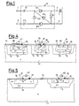
- pilot circuit P equipped with pilot input terminals 1 and 2 and output terminals 3 and 4 is shown assigned to gate piloting of an MOS power transistor T.
- the pilot circuit includes two condensers C1, C2 placed on the two input terminals 1, 2 for decoupling between the input signal and the transistor T, a 4-diode system D1-D4 with rectifying functions and a resistor R placed between the two output terminals 3, 4 to shunt and thus eliminate any interference which could otherwise reach the gate of the transistor T by the capacitive way and cause self ignition of said transistor.
- the diodes D1-D4 are selected in such a manner as to hold an inverse voltage of over 15V.
- the resistor R is selected between 75 and 500 kohm.
- the condensers C1 and C2 are selected in such a manner as to have a capacitance greater than 10pF.
- the input signal consists of a pair of complementary square waves with a frequency around 1MHz and amplitude around 10V.
- Said pilot circuit can also be used to control two MOS power transistors connected with a common source or drain to accomplish an alternating current switch or to control the higher part of an MOS power transistor semibridge.
- FIGS. 2-4 show how said pilot circuit can be accomplished in an integrated structure in accordance with the present invention.
- a semiconductor substrate 11 with N doping (optionally provided with one or more epitaxial strata in accordance with the known art) there are accomplished for the various circuital components (C1, C2; D1-D4; R) respective electrically floating insulation recesses 12 of type P+ inside of which are formed the same components by diffusion of types N and P dopes.
- each diode D1-D4 includes a type N+ buried layer 13 which communicates with the surface of the substrate (covered with oxide 14) through sinker regions 15. Inside the N+ doped area formed by the buried layer 13 and the contact regions 15 with the interposition of an N ⁇ doped area there is accomplished a P area 17. The two areas 15 and 17 can be reached through surface contacts 18 and 19 and constitute the two terminals of the diode symbolized in dot and dash lines in the aforesaid figures.
- each condenser C1-C2 includes an N+ doped buried layer 21, an intermediate N ⁇ doped area 22 and an N+ doped surface area 23.
- This last area, which can be reached through a surface contact 24, constitutes one of the condenser plates while the other is made up of a surface metallization 25 placed on a portion of the oxide 14 which constitutes the condenser dielectric.
- the condenser is symbolized in dash and dot lines.
- the resistor R illustrated in FIGS. 2 and 4 calls for an N+ doped buried layer 31, an N ⁇ doped intermediate layer 32 and a P doped surface area 33 accomplished in coil form as shown in FIG. 2.
- the buried layers 13, 21, 31 and the sinker regions 15 can be lacking so that the diodes D1-D4, the condensers C1-C2 and the resistor R can assume the form shown in FIG. 5 (for the diodes D1 and D2).
- each of the doped layers described above can be doped in the opposite manner, i.e. N doping instead of P doping and vice versa and the substrate 11 can be type P and the recess 12 type N.
- the overall capacitance between one component and the next is given by the series of capacitances between the individual component and the respective recess 12 and between the latter and the substrate 11, i.e. it is halved in relation to the conventional integration technique without insulating recesses.
- the pilot circuit shown in FIGS. 2-4 or 5 operates in such a manner that a 10V square wave signal at the input and with a frequency of 1MHz can allow reaching the continuous 8V at the gate of an MOS power transistor with input capacity of 600pF.
- the integrated structure in accordance with the invention i.e. with an insulating recess for each component, is employable not only for pilot circuits but in general for signal transfer networks.
- the components employed can be diodes, condensers, resistors or even transistors of any type.
- the need can arise to capacitively decouple active components like bipolar transistors (NPN or PNP) or MOS transistors (N channel or P channel), forming part of circuits which require low cross-talk.
- active components like bipolar transistors (NPN or PNP) or MOS transistors (N channel or P channel), forming part of circuits which require low cross-talk.
- the transistors to be separated e.g. the two input transistors of two associated amplifiers, can be accomplished in an integrated structure in accordance with the present invention.
- two bipolar transistors T1-T2 can be formed in a single semiconductor substrate 11 with N+ doping, provided with an N ⁇ epitaxial layer 41 covered with oxide 51.
- Each transistor is enclosed in a respective P+ electrically floating insulation recess 12 and comprises an N+ buried layer 43, an N ⁇ doped intermediate area and surface areas 45, 46, 47 of which the first two are N+ doped and the third is P doped enclosing said area 46.
- Electrical contacts 48 and 49 pass through the oxide layer 51 until they reach the N+ areas 45 and 46 to constitute the collector and emitter terminals of the transistor. In a similar manner an electrical contact 50 reaches the P area 47 to constitute the base terminal of said transistor.
- FIG. 7 An integrated structure in accordance with the invention comprising two MOS transistors is shown in FIG. 7 where reference number 11 indicates an N+ substrate provided with an N ⁇ epitaxial layer 61 and an overlying oxide layer 62.
- Each transistor is formed inside a respective electrically floating P+ insulation recess 12 and comprises an N+ buried layer 64, an N ⁇ intermediate area 65 and surface areas 66, 67 and 68 of which the first two are N+ and the third is P+ enclosing said area 67.
- Electrical contacts 69 and 70 pass through the oxide layer 62 until the first reaches the area 66 and the second the side by side areas 67 and 68 to constitute respectively the drain and source terminals of the transistor.
- a strip of polysilicon 71 is overlaid on the surface areas 67 and 68 between the two contacts 69 and 70 over part of the oxide layer 62 to constitute the gate terminal of the transistor.
Landscapes
- Engineering & Computer Science (AREA)
- Physics & Mathematics (AREA)
- Condensed Matter Physics & Semiconductors (AREA)
- General Physics & Mathematics (AREA)
- Manufacturing & Machinery (AREA)
- Computer Hardware Design (AREA)
- Microelectronics & Electronic Packaging (AREA)
- Power Engineering (AREA)
- Metal-Oxide And Bipolar Metal-Oxide Semiconductor Integrated Circuits (AREA)
- Bipolar Transistors (AREA)
- Bipolar Integrated Circuits (AREA)
Applications Claiming Priority (2)
| Application Number | Priority Date | Filing Date | Title |
|---|---|---|---|
| IT19593/87A IT1218128B (it) | 1987-03-05 | 1987-03-05 | Struttura integrata per rete di trasferimento di segnali,particolarmente per circuito di pilotaggio per transistori mos di potenza |
| IT1959387 | 1987-03-05 |
Publications (1)
| Publication Number | Publication Date |
|---|---|
| EP0283066A1 true EP0283066A1 (de) | 1988-09-21 |
Family
ID=11159312
Family Applications (1)
| Application Number | Title | Priority Date | Filing Date |
|---|---|---|---|
| EP88200290A Ceased EP0283066A1 (de) | 1987-03-05 | 1988-02-18 | Integrierte Struktur für ein Signalübertragungsnetzwerk, insbesondere für einen Pilotschaltkreis für MOS-Leistungstransistoren |
Country Status (4)
| Country | Link |
|---|---|
| US (1) | US4969030A (de) |
| EP (1) | EP0283066A1 (de) |
| JP (1) | JPS63228659A (de) |
| IT (1) | IT1218128B (de) |
Cited By (3)
| Publication number | Priority date | Publication date | Assignee | Title |
|---|---|---|---|---|
| GB2240951A (en) * | 1990-02-09 | 1991-08-21 | Canon Kk | Integrated transducer and semiconductor circuit arrays in thermal ink jet printers. |
| EP0491217A1 (de) * | 1990-12-19 | 1992-06-24 | Siemens Aktiengesellschaft | Integrierte Transistor-Freilaufdioden-Anordnung |
| EP0685891A1 (de) * | 1994-05-31 | 1995-12-06 | STMicroelectronics S.r.l. | Integrierte Halbleiterdiode |
Families Citing this family (13)
| Publication number | Priority date | Publication date | Assignee | Title |
|---|---|---|---|---|
| USRE35642E (en) * | 1987-12-22 | 1997-10-28 | Sgs-Thomson Microelectronics, S.R.L. | Integrated high-voltage bipolar power transistor and low voltage MOS power transistor structure in the emitter switching configuration and relative manufacturing process |
| IT1217323B (it) * | 1987-12-22 | 1990-03-22 | Sgs Microelettronica Spa | Struttura integrata di transistor bipolare di potenza di alta tensione e di transistor mos di potenza di bassa tensione nella configurazione"emitter switching"e relativo processo di fabbricazione |
| US5156989A (en) * | 1988-11-08 | 1992-10-20 | Siliconix, Incorporated | Complementary, isolated DMOS IC technology |
| IT1236667B (it) * | 1989-11-07 | 1993-03-25 | Sgs Thomson Microelectronics | Dispositivo di protezione contro la rottura di una regione diffusa di tipo n+ inserita in una struttura integrata di potenza a semiconduttore di tipo verticale |
| EP0513415A1 (de) * | 1991-05-16 | 1992-11-19 | Kabushiki Kaisha Toshiba | FET mit isoliertem Gate mit doppel-schichtigen Wannen von niedriger und höherer Störstoffkonzentrationen und sein Herstellungsverfahren |
| US5286995A (en) * | 1992-07-14 | 1994-02-15 | Texas Instruments Incorporated | Isolated resurf LDMOS devices for multiple outputs on one die |
| JP3918220B2 (ja) * | 1997-02-27 | 2007-05-23 | ソニー株式会社 | 半導体装置及びその製造方法 |
| US6502893B1 (en) | 2002-02-08 | 2003-01-07 | Lawrence M. Corliss, Jr. | Extendable deck assembly |
| US20130069157A1 (en) * | 2011-09-20 | 2013-03-21 | Alpha And Omega Semiconductor Incorporated | Semiconductor chip integrating high and low voltage devices |
| US20130071994A1 (en) * | 2011-09-20 | 2013-03-21 | Alpha And Omega Semiconductor Incorporated | Method of integrating high voltage devices |
| US20130069154A1 (en) * | 2011-09-20 | 2013-03-21 | Alpha And Omega Semiconductor Incorporated | Semiconductor chip integrating high and low voltage devices |
| US9214457B2 (en) * | 2011-09-20 | 2015-12-15 | Alpha & Omega Semiconductor Incorporated | Method of integrating high voltage devices |
| CN103515324B (zh) * | 2012-06-30 | 2016-10-26 | 万国半导体股份有限公司 | 集成高压器件的方法 |
Citations (3)
| Publication number | Priority date | Publication date | Assignee | Title |
|---|---|---|---|---|
| CH486127A (de) * | 1968-09-05 | 1970-02-15 | Ibm | Monolithische integrierte Halbleitervorrichtung |
| EP0117867A1 (de) * | 1982-08-26 | 1984-09-12 | Mitsubishi Denki Kabushiki Kaisha | Halbleitervorrichtung |
| FR2543364A1 (fr) * | 1983-03-25 | 1984-09-28 | Trt Telecom Radio Electr | Procede de realisation de transistors par integration monolithique en technologie bipolaire et circuits integres ainsi obtenus |
Family Cites Families (7)
| Publication number | Priority date | Publication date | Assignee | Title |
|---|---|---|---|---|
| JPS5279787A (en) * | 1975-12-26 | 1977-07-05 | Toshiba Corp | Integrated circuit device |
| JPS60124863A (ja) * | 1983-12-09 | 1985-07-03 | Nec Ic Microcomput Syst Ltd | Mos集積回路装置 |
| JPS60140844A (ja) * | 1983-12-28 | 1985-07-25 | Nec Corp | 半導体装置 |
| FR2571178B1 (fr) * | 1984-09-28 | 1986-11-21 | Thomson Csf | Structure de circuit integre comportant des transistors cmos a tenue en tension elevee, et son procede de fabrication |
| FR2571544B1 (fr) * | 1984-10-05 | 1987-07-31 | Haond Michel | Procede de fabrication d'ilots de silicium monocristallin isoles electriquement les uns des autres |
| US4648909A (en) * | 1984-11-28 | 1987-03-10 | Fairchild Semiconductor Corporation | Fabrication process employing special masks for the manufacture of high speed bipolar analog integrated circuits |
| US4651178A (en) * | 1985-05-31 | 1987-03-17 | Rca Corporation | Dual inverse zener diode with buried junctions |
-
1987
- 1987-03-05 IT IT19593/87A patent/IT1218128B/it active
-
1988
- 1988-02-18 EP EP88200290A patent/EP0283066A1/de not_active Ceased
- 1988-03-04 JP JP63049962A patent/JPS63228659A/ja active Pending
-
1990
- 1990-04-03 US US07/504,720 patent/US4969030A/en not_active Expired - Lifetime
Patent Citations (3)
| Publication number | Priority date | Publication date | Assignee | Title |
|---|---|---|---|---|
| CH486127A (de) * | 1968-09-05 | 1970-02-15 | Ibm | Monolithische integrierte Halbleitervorrichtung |
| EP0117867A1 (de) * | 1982-08-26 | 1984-09-12 | Mitsubishi Denki Kabushiki Kaisha | Halbleitervorrichtung |
| FR2543364A1 (fr) * | 1983-03-25 | 1984-09-28 | Trt Telecom Radio Electr | Procede de realisation de transistors par integration monolithique en technologie bipolaire et circuits integres ainsi obtenus |
Cited By (8)
| Publication number | Priority date | Publication date | Assignee | Title |
|---|---|---|---|---|
| GB2240951A (en) * | 1990-02-09 | 1991-08-21 | Canon Kk | Integrated transducer and semiconductor circuit arrays in thermal ink jet printers. |
| US5264874A (en) * | 1990-02-09 | 1993-11-23 | Canon Kabushiki Kaisha | Ink jet recording system |
| GB2240951B (en) * | 1990-02-09 | 1994-10-05 | Canon Kk | Ink jet recording system |
| US5567630A (en) * | 1990-02-09 | 1996-10-22 | Canon Kabushiki Kaisha | Method of forming an ink jet recording device, and head using same |
| EP0491217A1 (de) * | 1990-12-19 | 1992-06-24 | Siemens Aktiengesellschaft | Integrierte Transistor-Freilaufdioden-Anordnung |
| EP0685891A1 (de) * | 1994-05-31 | 1995-12-06 | STMicroelectronics S.r.l. | Integrierte Halbleiterdiode |
| US5629558A (en) * | 1994-05-31 | 1997-05-13 | Sgs-Thomson Microelectronics, S.Rl | Semiconductor diode integrated with bipolar/CMOS/DMOS technology |
| US5940700A (en) * | 1994-05-31 | 1999-08-17 | Sgs-Thomson Microelectronics, 2 Via C. Olivetti | Method for fabricating a semiconductor diode with BCD technology |
Also Published As
| Publication number | Publication date |
|---|---|
| IT1218128B (it) | 1990-04-12 |
| IT8719593A0 (it) | 1987-03-05 |
| US4969030A (en) | 1990-11-06 |
| JPS63228659A (ja) | 1988-09-22 |
Similar Documents
| Publication | Publication Date | Title |
|---|---|---|
| US4969030A (en) | Integrated structure for a signal transfer network, in particular for a pilot circuit for MOS power transistors | |
| US5801418A (en) | High voltage power integrated circuit with level shift operation and without metal crossover | |
| US20210367030A1 (en) | Device isolator with reduced parasitic capacitance | |
| US4314268A (en) | Integrated circuit with shielded lead patterns | |
| NO170177B (no) | System for fjernovervaakning av elevatoranlegg | |
| JP3520973B2 (ja) | 半導体装置 | |
| EP0615286B1 (de) | Halbleiteranordnung mit einer Isolationszone | |
| US4547791A (en) | CMOS-Bipolar Darlington device | |
| US5592015A (en) | Dielectric isolated type semiconductor device provided with bipolar element | |
| JPH02280621A (ja) | トランジスタ回路 | |
| US4423433A (en) | High-breakdown-voltage resistance element for integrated circuit with a plurality of multilayer, overlapping electrodes | |
| US4161742A (en) | Semiconductor devices with matched resistor portions | |
| EP0423791B1 (de) | MIS-Kapazitätselement | |
| US4631570A (en) | Integrated circuit having buried oxide isolation and low resistivity substrate for power supply interconnection | |
| KR100366897B1 (ko) | 반도체 장치 | |
| EP0117566A2 (de) | Halbleiteranordnung mit einem Koppelkondensator | |
| JPH01146352A (ja) | 能動及び受動素子を絶縁ポケット内に含み、各素子とそれを含むポケットの間での破壊電圧よりも高い電圧において動作する集積構造 | |
| US4649414A (en) | PNPN semiconductor switches | |
| KR100366896B1 (ko) | 반도체 장치 | |
| EP0961323B1 (de) | Integrierte CMOS Schaltung für Gebrauch bei hohen Frequenzen | |
| US4903095A (en) | Integrated circuit comprising a device for protection against electrostatic discharge | |
| US5466959A (en) | Semiconductor device for influencing the breakdown voltage of transistors | |
| KR0138917B1 (ko) | 반도체 소자 | |
| US4190778A (en) | A.C. supplied integrated semi-conductor logic circuit | |
| US5187562A (en) | Input protection structure for integrated circuits |
Legal Events
| Date | Code | Title | Description |
|---|---|---|---|
| PUAI | Public reference made under article 153(3) epc to a published international application that has entered the european phase |
Free format text: ORIGINAL CODE: 0009012 |
|
| AK | Designated contracting states |
Kind code of ref document: A1 Designated state(s): DE FR GB NL SE |
|
| 17P | Request for examination filed |
Effective date: 19890131 |
|
| RAP1 | Party data changed (applicant data changed or rights of an application transferred) |
Owner name: SGS-THOMSON MICROELECTRONICS S.R.L. |
|
| 17Q | First examination report despatched |
Effective date: 19910402 |
|
| STAA | Information on the status of an ep patent application or granted ep patent |
Free format text: STATUS: THE APPLICATION HAS BEEN REFUSED |
|
| 18R | Application refused |
Effective date: 19930828 |