EP0961323B1 - Integrierte CMOS Schaltung für Gebrauch bei hohen Frequenzen - Google Patents
Integrierte CMOS Schaltung für Gebrauch bei hohen Frequenzen Download PDFInfo
- Publication number
- EP0961323B1 EP0961323B1 EP99108509A EP99108509A EP0961323B1 EP 0961323 B1 EP0961323 B1 EP 0961323B1 EP 99108509 A EP99108509 A EP 99108509A EP 99108509 A EP99108509 A EP 99108509A EP 0961323 B1 EP0961323 B1 EP 0961323B1
- Authority
- EP
- European Patent Office
- Prior art keywords
- layer
- semiconductor substrate
- substrate
- components
- cmos circuit
- Prior art date
- Legal status (The legal status is an assumption and is not a legal conclusion. Google has not performed a legal analysis and makes no representation as to the accuracy of the status listed.)
- Expired - Lifetime
Links
- 239000000758 substrate Substances 0.000 claims description 39
- 239000004065 semiconductor Substances 0.000 claims description 25
- VYPSYNLAJGMNEJ-UHFFFAOYSA-N Silicium dioxide Chemical compound O=[Si]=O VYPSYNLAJGMNEJ-UHFFFAOYSA-N 0.000 claims description 5
- 239000011810 insulating material Substances 0.000 claims description 5
- 239000000463 material Substances 0.000 claims description 4
- 229910052581 Si3N4 Inorganic materials 0.000 claims description 3
- HQVNEWCFYHHQES-UHFFFAOYSA-N silicon nitride Chemical compound N12[Si]34N5[Si]62N3[Si]51N64 HQVNEWCFYHHQES-UHFFFAOYSA-N 0.000 claims description 3
- 239000000377 silicon dioxide Substances 0.000 claims description 2
- 235000012239 silicon dioxide Nutrition 0.000 claims description 2
- XUIMIQQOPSSXEZ-UHFFFAOYSA-N Silicon Chemical compound [Si] XUIMIQQOPSSXEZ-UHFFFAOYSA-N 0.000 description 4
- 238000000034 method Methods 0.000 description 4
- 229910052710 silicon Inorganic materials 0.000 description 4
- 239000010703 silicon Substances 0.000 description 4
- 239000003990 capacitor Substances 0.000 description 3
- 239000002800 charge carrier Substances 0.000 description 3
- 230000008878 coupling Effects 0.000 description 3
- 238000010168 coupling process Methods 0.000 description 3
- 238000005859 coupling reaction Methods 0.000 description 3
- 230000000694 effects Effects 0.000 description 3
- 230000005669 field effect Effects 0.000 description 3
- 230000004888 barrier function Effects 0.000 description 2
- 230000003071 parasitic effect Effects 0.000 description 2
- 229910001218 Gallium arsenide Inorganic materials 0.000 description 1
- 230000000740 bleeding effect Effects 0.000 description 1
- 150000001875 compounds Chemical class 0.000 description 1
- 239000004020 conductor Substances 0.000 description 1
- 239000013078 crystal Substances 0.000 description 1
- 230000008021 deposition Effects 0.000 description 1
- 238000005516 engineering process Methods 0.000 description 1
- 230000002349 favourable effect Effects 0.000 description 1
- 239000003574 free electron Substances 0.000 description 1
- 229910052732 germanium Inorganic materials 0.000 description 1
- GNPVGFCGXDBREM-UHFFFAOYSA-N germanium atom Chemical compound [Ge] GNPVGFCGXDBREM-UHFFFAOYSA-N 0.000 description 1
- 238000002513 implantation Methods 0.000 description 1
- 238000004519 manufacturing process Methods 0.000 description 1
- 230000000873 masking effect Effects 0.000 description 1
- 239000002184 metal Substances 0.000 description 1
- 229910021420 polycrystalline silicon Inorganic materials 0.000 description 1
- 229920005591 polysilicon Polymers 0.000 description 1
- 229910052814 silicon oxide Inorganic materials 0.000 description 1
- 239000002210 silicon-based material Substances 0.000 description 1
Images
Classifications
-
- H—ELECTRICITY
- H10—SEMICONDUCTOR DEVICES; ELECTRIC SOLID-STATE DEVICES NOT OTHERWISE PROVIDED FOR
- H10D—INORGANIC ELECTRIC SEMICONDUCTOR DEVICES
- H10D88/00—Three-dimensional [3D] integrated devices
Definitions
- the invention relates to an integrated CMOS circuit as claimed in claim 1.
- CMOS circuits produced by present-day conventional processes suffer from the disadvantage that the passive components required in the circuit, such as coils and capacitors, have a low Q-factor when used in typical high frequency applications such as input stages for symmetrical mixers or impedance transformers. This low Q-factor is attributable to undesirable capacitive coupling, and to the generation of eddy currents flowing in the conducting semiconductor substrate, made possible by the great number of charge carriers existing in such a semiconductor substrate.
- Passive components with a low Q-factor are not desirable in high frequency circuits, since they require the use of additional active stages, in order to compensate for the energy losses caused on account of the low Q-factor.
- the use of components with a low Q-factor results in increased noise figures.
- the use of passive components is unavoidable because the CMOS components present a strictly capacitive input impedance, so that normally a coil with a high inductivity must be used, for the purpose of impedance matching, which acts in series-resonance with the input capacitance of the MOS transistor.
- the low Q-factor with which the coil can be produced is of great disadvantage.
- US-A-5 559 349 discloses a silicon microwave monolithic integrated circuit device including a high-resistivity silicon substrate and a backside ground plane. A first area of the substrate is covered by a masking layer of low temperature silicon oxide, silicon nitride and polysilicon sublayers on which the passive devices are formed. On a second area of the substrate, a single-crystal epitaxial layer is deposited in which the active devices are formed.
- US-A-4,662,057 discloses a Bi-CMOS device which comprises a semiconductor substrate of p-type and an epitaxial layer of n-type grown on the surface of the semiconductor substrate. An n+ buried region is formed between the p- substrate and the n- epitaxial layer. In a first region of the epitaxial layer a bipolar element is formed, and in a second region of the epitaxial layer a CMOS device is formed, wherein the first and second regions are electrically isolated from each other.
- the aim of the invention is to provide an integrated CMOS circuit for use at high frequencies, wherein passive components with a high Q-factor can be produced by a simple and cost-effective process.
- this aim is achieved by providing an integrated CMOS circuit of the type mentioned above which has the features of claim 1.
- the integrated CMOS circuit according to the invention is formed in a high-resistance substrate with a conductive contact layer on the other side.
- the buried conductive layer created under the CMOS components that is the active components of the circuit, prevents undesirable latch-up effects caused by any parasitic thyristor action.
- This conductive buried layer does not exist under the passive components, to prevent this from being the cause of coupling with neighbouring components. It is no longer possible for eddy currents, induced by the passive components, to be created to a significant degree, as the required charge carriers are bled off through the conductive contact layer.
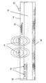
- FIG. 1 shows a schematic sectional view of a semiconductor substrate with an integrated CMOS circuit for use at high frequencies.
- the semiconductor component 10, shown in the drawing may consist of silicon, germanium, some other semi-conducting material, or even of a compound semiconductor such as GaAs. It must, however, be a material of high resistivity of 5 k ⁇ cm.
- Active components such as n-channel field effect transistors and p-channel field effect transistors, are formed in the upper surface of the semiconductor substrate 10 by means of conventional processes. Two of these field effect transistors are shown schematically under item 12 in the illustration. These active components are connected by connector paths, not shown here, to create the desired CMOS circuit.
- insulating layer 14 On top of the substrate 10 there is an insulating layer 14 on whose surface are formed passive components.
- the turns of a coil 16, as well as a conductor 18 of a micro strip line are shown as examples. Broken lines at the coil represent the field lines of a magnetic field caused by the coil, which may induce eddy currents in the semiconductor substrate 10.
- a capacitor 20 is formed in the layer 14.
- the insulating layer 14 may consist, for example of silicon dioxide or silicon nitride.
- the active and passive components only represent examples of components which are used in conventional high frequency circuits. It is obvious that other components may be included in the circuit, such as Schottky diodes, tunnel diodes or similar devices.
- a conducting layer 22 is buried in the high-Ohm semiconductor substrate 10 under the active components. This layer prevents any latch-up effect, that is the triggering of a parasitic thyristor forming under the active components, while certain potential conditions prevail.
- a contact layer 24 on the back of the semiconductor substrate 10 makes certain that the residual eddy currents induced in the semiconductor substrate are bled away, so that they cannot influence the behaviour of other components included in the circuit.
- the semiconductor substrate 10 may consist of either an n-type or a p-type semiconductor material.
- the p-type trough, in which the n-channel FETs are normally created may be set at any desired potential. This proves advantageous with RF amplifiers in common gate configuration.
- the buried conductive layer 22 may be created by implantation, by selective epitaxial growth deposition or by a combination of both processes. It is of the same conduction type as the substrate. It must have a markedly lower specific resistivity than the substrate of 0.1 ⁇ cm.
- the conducting contact layer 24 on the back of substrate 10 consists of a doped semiconductor layer of a conduction type opposed to that of the substrate 10.
- a barrier depletion layer is created between the substrate 10 and the contact layer 24. It may be arranged that this barrier layer creates a space charge region large enough to starve the entire substrate 10 of charge carriers, which will have a favourable effect as regards the RF behaviour of the passive components.
- the contact layer 24 of the circuit is connected to the positive supply line, when in operation, so ensuring that the free electrons occurring in the substrate 10 are bled away.
- the contact layer 24 is grounded for the purpose of bleeding away any free positive charges.
- Schottky diodes with a very low stray capacity may be created. It is therefore extremely advantageous to use these diodes as part of RF switching devices and bridge mixers. Furthermore, high quality impedance transformers may be produced, since the coils have the required high Q-factor. It is also easy to produce tunnel diodes, which may be used as third order frequency multipliers.
- CMOS circuit with RF components in a silicon substrate with a specific resistivity of approximately 5 k ⁇ cm, and a buried layer with a specific resistivity of 0.1 ⁇ cm was made up. Silicon material with a specific resistivity of approximately 0.01 ⁇ cm was used for the contact layer 24.
- coils with a Q-factor of 30 and capacitors with a Q-factor of 60 have been realised at a frequency of 2 GHz.
- Such a circuit is particularly suited to be used in a combination with a digital signal processor (DSP) on the same chip, because the same manufacturing process can be used for both parts of the circuit, that is to say the analogue RF section and the digital signal processing section.
- DSP digital signal processor
Landscapes
- Metal-Oxide And Bipolar Metal-Oxide Semiconductor Integrated Circuits (AREA)
- Semiconductor Integrated Circuits (AREA)
Claims (3)
- Integrierte CMOS-Schaltung zur Verwendung bei hohen Frequenzen, mit aktiven CMOS-Bauelementen und mit passiven Bauelementen, bei der die aktiven CMOS-Bauelemente (12) in einem Halbleitersubstrat (10) gebildet sind, das einen spezifischen Widerstand von 5 kΩcm hat, die passiven Bauelemente (16, 18, 20) in oder auf einer auf dem Halbleitersubstrat (10) angeordneten Schicht (14) aus Isoliermaterial gebildet sind, wobei eine leitfähige Schicht (22), die einen spezifischen Widerstand von 0,1 Ωcm hat und vom gleichen Leitungstyp wie das Substrat (10) ist, in dem Halbleitersubstrat (10) unter den aktiven CMOS-Bauelementen (12) und nicht unter den passiven Bauelementen (16, 18, 20) vergraben ist, und auf einer von der Schicht (14) aus Isoliermaterial abgewandten Fläche des Halbleitersubstrats (10) eine leitende Kontaktschicht (24) gebildet ist, wobei die leitende Kontaktschicht (24) eine dotierte Halbleiterschicht ist, die aus Material vom entgegengesetzten Leitungstyp wie das Halbleitersubstrat (10) ist.
- Integrierte CMOS-Schaltung nach Anspruch 1, bei der die Schicht (14) aus Isoliermaterial aus Siliciumdioxid besteht.
- Integrierte CMOS-Schaltung nach Anspruch 1, bei der die Schicht (14) aus Isoliermaterial aus Siliciumnitrid besteht.
Applications Claiming Priority (2)
| Application Number | Priority Date | Filing Date | Title |
|---|---|---|---|
| DE19821726 | 1998-05-14 | ||
| DE19821726A DE19821726C1 (de) | 1998-05-14 | 1998-05-14 | Ingegrierte CMOS-Schaltung für die Verwendung bei hohen Frequenzen |
Publications (3)
| Publication Number | Publication Date |
|---|---|
| EP0961323A2 EP0961323A2 (de) | 1999-12-01 |
| EP0961323A3 EP0961323A3 (de) | 2000-09-13 |
| EP0961323B1 true EP0961323B1 (de) | 2009-07-08 |
Family
ID=7867810
Family Applications (1)
| Application Number | Title | Priority Date | Filing Date |
|---|---|---|---|
| EP99108509A Expired - Lifetime EP0961323B1 (de) | 1998-05-14 | 1999-05-03 | Integrierte CMOS Schaltung für Gebrauch bei hohen Frequenzen |
Country Status (4)
| Country | Link |
|---|---|
| US (1) | US6348718B1 (de) |
| EP (1) | EP0961323B1 (de) |
| JP (1) | JP2000082748A (de) |
| DE (2) | DE19821726C1 (de) |
Families Citing this family (8)
| Publication number | Priority date | Publication date | Assignee | Title |
|---|---|---|---|---|
| SE515831C2 (sv) * | 1999-02-15 | 2001-10-15 | Ericsson Telefon Ab L M | Halvledaranordning med induktor och förfarande vid framställning av en sådan halvledaranordning |
| US6545338B1 (en) * | 1999-10-28 | 2003-04-08 | Koninklijke Philips Electronics N.V. | Methods for implementing co-axial interconnect lines in a CMOS process for high speed RF and microwave applications |
| US6621139B2 (en) * | 2001-12-31 | 2003-09-16 | Taiwan Semiconductor Manufacturing Co., Ltd | Method for fabricating a tunable, 3-dimensional solenoid and device fabricated |
| US7304354B2 (en) | 2004-02-17 | 2007-12-04 | Silicon Space Technology Corp. | Buried guard ring and radiation hardened isolation structures and fabrication methods |
| US8901703B2 (en) * | 2004-05-06 | 2014-12-02 | Nxp, B.V. | Electronic device |
| US8278719B2 (en) * | 2005-10-14 | 2012-10-02 | Silicon Space Technology Corp. | Radiation hardened isolation structures and fabrication methods |
| JP4878502B2 (ja) * | 2006-05-29 | 2012-02-15 | ルネサスエレクトロニクス株式会社 | 半導体装置 |
| US10038058B2 (en) | 2016-05-07 | 2018-07-31 | Silicon Space Technology Corporation | FinFET device structure and method for forming same |
Family Cites Families (13)
| Publication number | Priority date | Publication date | Assignee | Title |
|---|---|---|---|---|
| JPS5931052A (ja) * | 1982-08-13 | 1984-02-18 | Hitachi Ltd | 半導体集積回路装置の製造方法 |
| US4929570A (en) * | 1986-10-06 | 1990-05-29 | National Semiconductor Corporation | Selective epitaxy BiCMOS process |
| JPH07112024B2 (ja) * | 1988-11-10 | 1995-11-29 | 株式会社東芝 | 半導体装置 |
| JP2661318B2 (ja) * | 1990-03-27 | 1997-10-08 | 日本電気株式会社 | 半導体装置 |
| JP2950009B2 (ja) * | 1992-02-26 | 1999-09-20 | 日本電気株式会社 | BiCMOS集積回路装置及びその製造方法 |
| US5286991A (en) * | 1992-08-26 | 1994-02-15 | Pioneer Semiconductor Corporation | Capacitor for a BiCMOS device |
| KR940018967A (ko) * | 1993-01-30 | 1994-08-19 | 오가 노리오 | 반도체장치 및 그 제조방법 |
| US5370766A (en) * | 1993-08-16 | 1994-12-06 | California Micro Devices | Methods for fabrication of thin film inductors, inductor networks and integration with other passive and active devices |
| JP2874550B2 (ja) * | 1994-04-21 | 1999-03-24 | 日本電気株式会社 | 半導体集積回路装置 |
| US5559349A (en) * | 1995-03-07 | 1996-09-24 | Northrop Grumman Corporation | Silicon integrated circuit with passive devices over high resistivity silicon substrate portion, and active devices formed in lower resistivity silicon layer over the substrate |
| US5578860A (en) * | 1995-05-01 | 1996-11-26 | Motorola, Inc. | Monolithic high frequency integrated circuit structure having a grounded source configuration |
| JP3535615B2 (ja) * | 1995-07-18 | 2004-06-07 | 株式会社ルネサステクノロジ | 半導体集積回路装置 |
| JPH10303372A (ja) * | 1997-01-31 | 1998-11-13 | Sanyo Electric Co Ltd | 半導体集積回路およびその製造方法 |
-
1998
- 1998-05-14 DE DE19821726A patent/DE19821726C1/de not_active Expired - Fee Related
-
1999
- 1999-05-03 DE DE69941076T patent/DE69941076D1/de not_active Expired - Lifetime
- 1999-05-03 EP EP99108509A patent/EP0961323B1/de not_active Expired - Lifetime
- 1999-05-14 US US09/312,511 patent/US6348718B1/en not_active Expired - Lifetime
- 1999-05-14 JP JP11171459A patent/JP2000082748A/ja active Pending
Also Published As
| Publication number | Publication date |
|---|---|
| DE19821726C1 (de) | 1999-09-09 |
| JP2000082748A (ja) | 2000-03-21 |
| EP0961323A3 (de) | 2000-09-13 |
| EP0961323A2 (de) | 1999-12-01 |
| US6348718B1 (en) | 2002-02-19 |
| DE69941076D1 (de) | 2009-08-20 |
Similar Documents
| Publication | Publication Date | Title |
|---|---|---|
| US5514612A (en) | Method of making a semiconductor device with integrated RC network and schottky diode | |
| US7732293B2 (en) | Tunable semiconductor diodes | |
| US7022566B2 (en) | Integrated radio frequency circuits | |
| US20180358352A1 (en) | Structure, method, and circuit for electrostatic discharge protection utilizing a rectifying contact | |
| US5559349A (en) | Silicon integrated circuit with passive devices over high resistivity silicon substrate portion, and active devices formed in lower resistivity silicon layer over the substrate | |
| US5565701A (en) | Integrated circuit with vertical bipolar power transistors and isolated lateral bipolar control transistors | |
| US20190043855A1 (en) | LINEARITY AND LATERAL ISOLATION IN A BiCMOS PROCESS THROUGH COUNTER-DOPING OF EPITAXIAL SILICON REGION | |
| US6903459B2 (en) | High frequency semiconductor device | |
| US5623159A (en) | Integrated circuit isolation structure for suppressing high-frequency cross-talk | |
| US5706163A (en) | ESD-protected thin film capacitor structures | |
| US6791810B2 (en) | Protection circuit of field effect transistor and semiconductor device | |
| EP1391989A1 (de) | Abstimmschaltung und IGFET | |
| US4969030A (en) | Integrated structure for a signal transfer network, in particular for a pilot circuit for MOS power transistors | |
| US6348718B1 (en) | Integrated CMOS circuit for use at high frequencies | |
| US4721985A (en) | Variable capacitance element controllable by a D.C. voltage | |
| US20030234438A1 (en) | Integrated circuit structure for mixed-signal RF applications and circuits | |
| KR100366896B1 (ko) | 반도체 장치 | |
| CN112074953B (zh) | 集成电路装置及制造该集成电路装置的方法 | |
| SE509780C2 (sv) | Bipolär effekttransistor och framställningsförfarande | |
| US6291859B1 (en) | Integrated circuits | |
| CN119318000B (en) | Back gate effect control via doping | |
| KR102839538B1 (ko) | 도핑을 통한 백-게이트 효과 제어 | |
| EP4053889A1 (de) | Isolierte brunnen für verbesserte rauschleistung | |
| KR100794151B1 (ko) | 전계 효과 트랜지스터의 보호 회로 및 반도체 장치 | |
| WO2024248892A1 (en) | Field-plated resistor |
Legal Events
| Date | Code | Title | Description |
|---|---|---|---|
| PUAI | Public reference made under article 153(3) epc to a published international application that has entered the european phase |
Free format text: ORIGINAL CODE: 0009012 |
|
| AK | Designated contracting states |
Kind code of ref document: A2 Designated state(s): DE FR GB IT NL |
|
| AX | Request for extension of the european patent |
Free format text: AL;LT;LV;MK;RO;SI |
|
| PUAL | Search report despatched |
Free format text: ORIGINAL CODE: 0009013 |
|
| AK | Designated contracting states |
Kind code of ref document: A3 Designated state(s): AT BE CH CY DE DK ES FI FR GB GR IE IT LI LU MC NL PT SE |
|
| AX | Request for extension of the european patent |
Free format text: AL;LT;LV;MK;RO;SI |
|
| AKX | Designation fees paid |
Free format text: DE FR GB IT NL |
|
| 17P | Request for examination filed |
Effective date: 20010605 |
|
| 17Q | First examination report despatched |
Effective date: 20020327 |
|
| 17Q | First examination report despatched |
Effective date: 20020327 |
|
| GRAP | Despatch of communication of intention to grant a patent |
Free format text: ORIGINAL CODE: EPIDOSNIGR1 |
|
| GRAS | Grant fee paid |
Free format text: ORIGINAL CODE: EPIDOSNIGR3 |
|
| GRAA | (expected) grant |
Free format text: ORIGINAL CODE: 0009210 |
|
| AK | Designated contracting states |
Kind code of ref document: B1 Designated state(s): DE FR GB IT NL |
|
| REG | Reference to a national code |
Ref country code: GB Ref legal event code: FG4D |
|
| REF | Corresponds to: |
Ref document number: 69941076 Country of ref document: DE Date of ref document: 20090820 Kind code of ref document: P |
|
| NLV1 | Nl: lapsed or annulled due to failure to fulfill the requirements of art. 29p and 29m of the patents act | ||
| PG25 | Lapsed in a contracting state [announced via postgrant information from national office to epo] |
Ref country code: NL Free format text: LAPSE BECAUSE OF FAILURE TO SUBMIT A TRANSLATION OF THE DESCRIPTION OR TO PAY THE FEE WITHIN THE PRESCRIBED TIME-LIMIT Effective date: 20090708 |
|
| PLBE | No opposition filed within time limit |
Free format text: ORIGINAL CODE: 0009261 |
|
| STAA | Information on the status of an ep patent application or granted ep patent |
Free format text: STATUS: NO OPPOSITION FILED WITHIN TIME LIMIT |
|
| 26N | No opposition filed |
Effective date: 20100409 |
|
| PG25 | Lapsed in a contracting state [announced via postgrant information from national office to epo] |
Ref country code: IT Free format text: LAPSE BECAUSE OF FAILURE TO SUBMIT A TRANSLATION OF THE DESCRIPTION OR TO PAY THE FEE WITHIN THE PRESCRIBED TIME-LIMIT Effective date: 20090708 |
|
| PGFP | Annual fee paid to national office [announced via postgrant information from national office to epo] |
Ref country code: DE Payment date: 20120531 Year of fee payment: 14 |
|
| PG25 | Lapsed in a contracting state [announced via postgrant information from national office to epo] |
Ref country code: DE Free format text: LAPSE BECAUSE OF NON-PAYMENT OF DUE FEES Effective date: 20111130 |
|
| REG | Reference to a national code |
Ref country code: DE Ref legal event code: R119 Ref document number: 69941076 Country of ref document: DE Effective date: 20111201 |
|
| PGFP | Annual fee paid to national office [announced via postgrant information from national office to epo] |
Ref country code: GB Payment date: 20140425 Year of fee payment: 16 |
|
| PGFP | Annual fee paid to national office [announced via postgrant information from national office to epo] |
Ref country code: FR Payment date: 20140424 Year of fee payment: 16 |
|
| GBPC | Gb: european patent ceased through non-payment of renewal fee |
Effective date: 20150503 |
|
| REG | Reference to a national code |
Ref country code: FR Ref legal event code: ST Effective date: 20160129 |
|
| PG25 | Lapsed in a contracting state [announced via postgrant information from national office to epo] |
Ref country code: GB Free format text: LAPSE BECAUSE OF NON-PAYMENT OF DUE FEES Effective date: 20150503 |
|
| PG25 | Lapsed in a contracting state [announced via postgrant information from national office to epo] |
Ref country code: FR Free format text: LAPSE BECAUSE OF NON-PAYMENT OF DUE FEES Effective date: 20150601 |