EP0282124A2 - Verfahren zum Herstellen einer Modul-Halbleiter-Leistungsanordnung und hergestellte Anordnung - Google Patents
Verfahren zum Herstellen einer Modul-Halbleiter-Leistungsanordnung und hergestellte Anordnung Download PDFInfo
- Publication number
- EP0282124A2 EP0282124A2 EP88200374A EP88200374A EP0282124A2 EP 0282124 A2 EP0282124 A2 EP 0282124A2 EP 88200374 A EP88200374 A EP 88200374A EP 88200374 A EP88200374 A EP 88200374A EP 0282124 A2 EP0282124 A2 EP 0282124A2
- Authority
- EP
- European Patent Office
- Prior art keywords
- chips
- aforesaid
- terminals
- manufacturing
- plate
- Prior art date
- Legal status (The legal status is an assumption and is not a legal conclusion. Google has not performed a legal analysis and makes no representation as to the accuracy of the status listed.)
- Granted
Links
Images

Classifications
-
- H—ELECTRICITY
- H10—SEMICONDUCTOR DEVICES; ELECTRIC SOLID-STATE DEVICES NOT OTHERWISE PROVIDED FOR
- H10W—GENERIC PACKAGES, INTERCONNECTIONS, CONNECTORS OR OTHER CONSTRUCTIONAL DETAILS OF DEVICES COVERED BY CLASS H10
- H10W90/00—Package configurations
- H10W90/811—Multiple chips on leadframes
-
- H—ELECTRICITY
- H10—SEMICONDUCTOR DEVICES; ELECTRIC SOLID-STATE DEVICES NOT OTHERWISE PROVIDED FOR
- H10W—GENERIC PACKAGES, INTERCONNECTIONS, CONNECTORS OR OTHER CONSTRUCTIONAL DETAILS OF DEVICES COVERED BY CLASS H10
- H10W90/00—Package configurations
-
- H—ELECTRICITY
- H10—SEMICONDUCTOR DEVICES; ELECTRIC SOLID-STATE DEVICES NOT OTHERWISE PROVIDED FOR
- H10W—GENERIC PACKAGES, INTERCONNECTIONS, CONNECTORS OR OTHER CONSTRUCTIONAL DETAILS OF DEVICES COVERED BY CLASS H10
- H10W95/00—Packaging processes not covered by the other groups of this subclass
-
- Y—GENERAL TAGGING OF NEW TECHNOLOGICAL DEVELOPMENTS; GENERAL TAGGING OF CROSS-SECTIONAL TECHNOLOGIES SPANNING OVER SEVERAL SECTIONS OF THE IPC; TECHNICAL SUBJECTS COVERED BY FORMER USPC CROSS-REFERENCE ART COLLECTIONS [XRACs] AND DIGESTS
- Y10—TECHNICAL SUBJECTS COVERED BY FORMER USPC
- Y10T—TECHNICAL SUBJECTS COVERED BY FORMER US CLASSIFICATION
- Y10T29/00—Metal working
- Y10T29/49—Method of mechanical manufacture
- Y10T29/49002—Electrical device making
- Y10T29/49117—Conductor or circuit manufacturing
- Y10T29/49124—On flat or curved insulated base, e.g., printed circuit, etc.
- Y10T29/4913—Assembling to base an electrical component, e.g., capacitor, etc.
-
- Y—GENERAL TAGGING OF NEW TECHNOLOGICAL DEVELOPMENTS; GENERAL TAGGING OF CROSS-SECTIONAL TECHNOLOGIES SPANNING OVER SEVERAL SECTIONS OF THE IPC; TECHNICAL SUBJECTS COVERED BY FORMER USPC CROSS-REFERENCE ART COLLECTIONS [XRACs] AND DIGESTS
- Y10—TECHNICAL SUBJECTS COVERED BY FORMER USPC
- Y10T—TECHNICAL SUBJECTS COVERED BY FORMER US CLASSIFICATION
- Y10T29/00—Metal working
- Y10T29/49—Method of mechanical manufacture
- Y10T29/49002—Electrical device making
- Y10T29/49117—Conductor or circuit manufacturing
- Y10T29/49124—On flat or curved insulated base, e.g., printed circuit, etc.
- Y10T29/4913—Assembling to base an electrical component, e.g., capacitor, etc.
- Y10T29/49146—Assembling to base an electrical component, e.g., capacitor, etc. with encapsulating, e.g., potting, etc.
Definitions
- This invention concerns a method for manufacturing a modular semiconductor power device and the device obtained by means of such a method.
- the known semiconductor power devices involve complex and costly procedures, both from the point of view of the individual components necessary for constructing them and from the standpoint of their assembly and reciprocal insulation.
- the purpose of this invention is to provide a particularly reliable modular power device obtained by means of an extremely simple and not much expensive assembling procedure, according to a highly flexible manufacturing method and with components which, although extremely limited in number, can be used to create various circuit arrangements and layouts, always using the same tools and always keeping an identical external geometrical configuration of the devices obtained.
- the manufacturing method concerns a modular semiconductor power device comprising one or more semiconductor chips, a metal plate (11) for dissipating heat generated by Joule effect, a pluraliy of electrodes constituting the signal and power terminals of the device, and a resin encapsulation, and is characterized by the following steps: - soldering the chip/s onto one or more plates (33) of electrically conductive material; - positioning the plate/s (33) on a plane substantially parallel to the aforesaid heat dissipating plate (11) and close to the latter; -blanking, from a single sheet of conductive material, a one-piece frame (51) designed to constitute the power and signal terminals, said blanking enabling temporary connections (61) to be kept between the portions of the terminal conductors designed to remain outside of the resin encapsulation;
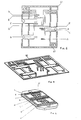
- reference 11 indicates the base plate of the device which, since it has to act as a heat sink as well as a support and fastener for the device itself, is made of heat-conductive metal with high mechanical strength.
- the holes A in it serve to secure it, by means of screws, onto the external heat spreader, while the grooves V serve to absorb any possible deformation of the base plate due to the high tightening torque, thereby preventing them from being transmitted to the central portion of the plate.
- the S-shaped drawings M on the sides (see the side and cross-sectional views of the plate shown in Figs. 2a and 2b ) serve to ensure a better grip of the subsequent resin encapsulation, as is explained more clearly further one with reference to figure 8b.
- Figure 1 also shows the components 12 and 13, which are two chip-supporting substrates, which are soldered onto the base plate 11 by means of the layers of solder 14.
- each substrate is composed of a quadrangular-shaped thin medial layer 31 of alumina (less than 1 mm thick), with thin copper plates soldered directly onto its two lateral faces.
- soldered onto the face destined to lie facing the upper face of the base plate 11 is a single copper plate 32, which is also quadrangular in shape but with slightly smaller dimensions than those of the layer of alumina, while the other face is provided with a rectangular plate 33, for supporting the chips and for the connections with an external electrode, and, on either side of said plate 33, narrower plates (lateral strips) 34, 35 and 36 designed both for soldering the conductor for connection with the chips, and for soldering other external electrodes.
- Figure 4 shows the device (41) as it appears after the two substrates have been soldered onto the base plate, the chips have been soldered onto the larger upper copper plates b and f, and the electrical connections have been carried out between the chips and the lateral strips a, c, d, e, g, h.
- the latter connections are obtained by ultrasound soldering of aluminium wire.
- Figure 5 shows a copper frame 51 designed to constitute the external terminals and the connections of the latter with the lateral strips and the plates f and b of figure 4.
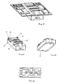
- the frame of figure 5 is obtained by blanking from a copper sheet and by subsequently bending the terminal portions downwards, said terminal portions being subsequently soldered onto the lateral strips and the plates f and b.
- Figure 6 shows a plan view of the frame of figure 5, as it appears after being blanked from the copper sheet and before the bending of the terminal portions, which are indicated respectively by h, g, e, d, c, a, f, b. After being bent downwards, said terminal portions are then soldered respectively onto the strips h, g, e, d, c, a, and onto the plates f and b of 41. After the frame 51 has been soldered onto the device 41, the device is encapsulated by means of a moulding process with insulating resin (e.g. thermosetting epoxy resin), preferably of the low-stress type. After the moulding phase, the device appears as shown in Figure 7 .
- insulating resin e.g. thermosetting epoxy resin
- the resin encapsulation ends, from below, flush with the lower surface of the base plate 11, which can consequently be secured in direct contact with the supporting metal structure on which it is designed to be placed, thereby ensuring efficient dissipation of the heat.
- the same figure clearly shows the function of the S-shaped drawings on the base plate (see figs. 1 and 2b). In fact, on completion of the device, they are completely embedded in the resin body, so as to constitute two areas for anchoring and ensuring an efficient grip of the resin.
- the procedures for soldering the conductors connecting the chips to the metal strips and the external electrodes to the metal chip-supporting strips or plates are simplified due to the flat disposition of the soldering points and to the fact that the inner ends of the electrodes are soldered when they are still firmly secured to each other by the aforesaid temporary connections; - due to the fact that the chips are soldered onto coplanar plates and to the presence of the temporary connections between the electrodes it is also possible to carry out the encapsulations and reciprocal insulation of the electrodes in a single step.
- a further advantage in addition to those mentioned pre strictlyviously, consists of that related to the particular structure of the substrate chosen for soldering the chips as well as that relates to the type of resin used for the encapsulation.
- said substrates which consist of a layer of alumina with copper plates soldered directly onto both faces, are characterized by thermal expansion coefficients very similar to those of silicon.
- thermomechanical stress which would otherwise be transmitted to the chips due to the differential expansions of silicon and copper
- other embodiments envisage the insertion, between the chips and the supporting copper plates, of layers of material, such as for example molybdenum, having an expan sion coefficient lying half way between those of silicon and copper, which however, complicate the assembling and lower the thermal performance).
- the wires connecting the chips to the metal strips of the substrates can be substituted by direct soldering between the inner terminal portions of the one-piece frame and the chips, whenever the latter have wettable metal coatings.
- These internal portions can then be soldered to points (P) of connection with the chips situated on the aforesaid plates 33 and strips 34, 35, 36 (as in the case illustrated in Figs. 4 and 5), or situated on the same plates and on wettable metal coatings on the surface of the chips.
- the chip-supporting substrates could have a different structure from that previously described and the insulation between the chips and the dissipator could be achieved by means of a layer of the encapsulating resin itself - which in this case should be of high thermal conductivity - instead of by a layer of alumina.
Landscapes
- Structures Or Materials For Encapsulating Or Coating Semiconductor Devices Or Solid State Devices (AREA)
- Cooling Or The Like Of Semiconductors Or Solid State Devices (AREA)
Applications Claiming Priority (2)
| Application Number | Priority Date | Filing Date | Title |
|---|---|---|---|
| IT19630/87A IT1202657B (it) | 1987-03-09 | 1987-03-09 | Procedimento di fabbricazione di un dispositivo modulare di potenza a semiconduttore e dispositivo con esso ottenento |
| IT1963087 | 1987-03-09 |
Publications (3)
| Publication Number | Publication Date |
|---|---|
| EP0282124A2 true EP0282124A2 (de) | 1988-09-14 |
| EP0282124A3 EP0282124A3 (en) | 1989-03-22 |
| EP0282124B1 EP0282124B1 (de) | 1993-09-15 |
Family
ID=11159882
Family Applications (1)
| Application Number | Title | Priority Date | Filing Date |
|---|---|---|---|
| EP88200374A Expired - Lifetime EP0282124B1 (de) | 1987-03-09 | 1988-02-29 | Verfahren zum Herstellen einer Modul-Halbleiter-Leistungsanordnung und hergestellte Anordnung |
Country Status (5)
| Country | Link |
|---|---|
| US (4) | US4926547A (de) |
| EP (1) | EP0282124B1 (de) |
| JP (1) | JPS6425732A (de) |
| DE (1) | DE3884019T2 (de) |
| IT (1) | IT1202657B (de) |
Cited By (3)
| Publication number | Priority date | Publication date | Assignee | Title |
|---|---|---|---|---|
| DE3837920A1 (de) * | 1988-11-09 | 1990-05-10 | Semikron Elektronik Gmbh | Halbleiterelement |
| US4926547A (en) * | 1987-03-09 | 1990-05-22 | Sgs-Thomson Microelectronics S.P.A. | Method for manufacturing a modular semiconductor power device |
| EP0959494A4 (de) * | 1996-08-20 | 2001-02-07 | Hitachi Ltd | Halbleiter und verfahren zur herstellung |
Families Citing this family (8)
| Publication number | Priority date | Publication date | Assignee | Title |
|---|---|---|---|---|
| JP2504610B2 (ja) * | 1990-07-26 | 1996-06-05 | 株式会社東芝 | 電力用半導体装置 |
| US5233583A (en) * | 1990-12-19 | 1993-08-03 | General Electric Company | Tracking and reading system for an optical medium and medium for use therewith |
| JPH05166969A (ja) * | 1991-10-14 | 1993-07-02 | Fuji Electric Co Ltd | 半導体装置 |
| US5705848A (en) * | 1995-11-24 | 1998-01-06 | Asea Brown Boveri Ag | Power semiconductor module having a plurality of submodules |
| US5736432A (en) * | 1996-09-20 | 1998-04-07 | National Semiconductor Corporation | Lead frame with lead finger locking feature and method for making same |
| US6534851B1 (en) * | 2000-08-21 | 2003-03-18 | Agere Systems, Inc. | Modular semiconductor substrates |
| US8422243B2 (en) * | 2006-12-13 | 2013-04-16 | Stats Chippac Ltd. | Integrated circuit package system employing a support structure with a recess |
| CN118053822B (zh) * | 2024-04-16 | 2024-08-06 | 四川职业技术学院 | 一种电源管理芯片的封装结构及封装方法 |
Family Cites Families (21)
| Publication number | Priority date | Publication date | Assignee | Title |
|---|---|---|---|---|
| GB1255073A (en) * | 1969-05-20 | 1971-11-24 | Ferranti Ltd | Improvements relating to electrical circuit assemblies |
| US4026008A (en) * | 1972-10-02 | 1977-05-31 | Signetics Corporation | Semiconductor lead structure and assembly and method for fabricating same |
| US4106052A (en) * | 1975-04-19 | 1978-08-08 | Semikron Gesellschaft Fur Gleichrichterbau Und Elektronik M.B.H. | Semiconductor rectifier unit having a base plate with means for maintaining insulating wafers in a desired position |
| JPS5340991A (en) * | 1976-09-21 | 1978-04-13 | Hitachi Zosen Corp | Device for buffering rocked liquid load incylindrical tank of ship |
| US4102039A (en) * | 1977-02-14 | 1978-07-25 | Motorola, Inc. | Method of packaging electronic components |
| FR2495376A1 (fr) * | 1980-12-02 | 1982-06-04 | Thomson Csf | Boitiers pour composants semiconducteurs de puissance a cosses de type faston |
| US4396936A (en) * | 1980-12-29 | 1983-08-02 | Honeywell Information Systems, Inc. | Integrated circuit chip package with improved cooling means |
| US4518982A (en) * | 1981-02-27 | 1985-05-21 | Motorola, Inc. | High current package with multi-level leads |
| GB2099742B (en) * | 1981-06-05 | 1985-07-31 | Philips Electronic Associated | Bonding metals to non-metals |
| FR2524707B1 (fr) * | 1982-04-01 | 1985-05-31 | Cit Alcatel | Procede d'encapsulation de composants semi-conducteurs, et composants encapsules obtenus |
| US4615031A (en) * | 1982-07-27 | 1986-09-30 | International Standard Electric Corporation | Injection laser packages |
| JPS5968958A (ja) * | 1982-10-12 | 1984-04-19 | Mitsubishi Electric Corp | ゲ−トタ−ンオフサイリスタ組立体 |
| JPS59181627A (ja) * | 1983-03-31 | 1984-10-16 | Toshiba Corp | 半導体装置の製造方法 |
| JPS6092650A (ja) * | 1983-10-27 | 1985-05-24 | Toshiba Corp | 半導体装置 |
| US4722060A (en) * | 1984-03-22 | 1988-01-26 | Thomson Components-Mostek Corporation | Integrated-circuit leadframe adapted for a simultaneous bonding operation |
| JPS60239051A (ja) * | 1984-05-11 | 1985-11-27 | Mitsubishi Electric Corp | 半導体装置 |
| US4675989A (en) * | 1984-05-11 | 1987-06-30 | Amp Incorporated | Method of making an electrical circuit package |
| US4635356A (en) * | 1984-12-28 | 1987-01-13 | Kabushiki Kaisha Toshiba | Method of manufacturing a circuit module |
| IT1185410B (it) * | 1985-10-10 | 1987-11-12 | Sgs Microelettronica Spa | Metodo e contenitore perfezionato per dissipare il calore generato da una piastrina a circuito integrato |
| IT1202657B (it) * | 1987-03-09 | 1989-02-09 | Sgs Microelettronica Spa | Procedimento di fabbricazione di un dispositivo modulare di potenza a semiconduttore e dispositivo con esso ottenento |
| US4783428A (en) * | 1987-11-23 | 1988-11-08 | Motorola Inc. | Method of producing a thermogenetic semiconductor device |
-
1987
- 1987-03-09 IT IT19630/87A patent/IT1202657B/it active
-
1988
- 1988-02-29 DE DE88200374T patent/DE3884019T2/de not_active Expired - Fee Related
- 1988-02-29 EP EP88200374A patent/EP0282124B1/de not_active Expired - Lifetime
- 1988-03-09 JP JP63053848A patent/JPS6425732A/ja active Pending
-
1989
- 1989-06-27 US US07/373,647 patent/US4926547A/en not_active Ceased
-
1990
- 1990-01-09 US US07/462,544 patent/US5038198A/en not_active Ceased
-
1994
- 1994-01-21 US US08/184,783 patent/USRE38037E1/en not_active Expired - Lifetime
-
1995
- 1995-11-13 US US08/558,979 patent/USRE37416E1/en not_active Expired - Lifetime
Cited By (4)
| Publication number | Priority date | Publication date | Assignee | Title |
|---|---|---|---|---|
| US4926547A (en) * | 1987-03-09 | 1990-05-22 | Sgs-Thomson Microelectronics S.P.A. | Method for manufacturing a modular semiconductor power device |
| USRE37416E1 (en) * | 1987-03-09 | 2001-10-23 | Stmicroelectronics S.R.L. | Method for manufacturing a modular semiconductor power device |
| DE3837920A1 (de) * | 1988-11-09 | 1990-05-10 | Semikron Elektronik Gmbh | Halbleiterelement |
| EP0959494A4 (de) * | 1996-08-20 | 2001-02-07 | Hitachi Ltd | Halbleiter und verfahren zur herstellung |
Also Published As
| Publication number | Publication date |
|---|---|
| EP0282124B1 (de) | 1993-09-15 |
| US5038198A (en) | 1991-08-06 |
| USRE38037E1 (en) | 2003-03-18 |
| DE3884019D1 (de) | 1993-10-21 |
| EP0282124A3 (en) | 1989-03-22 |
| JPS6425732A (en) | 1989-01-27 |
| US4926547A (en) | 1990-05-22 |
| DE3884019T2 (de) | 1994-02-03 |
| IT1202657B (it) | 1989-02-09 |
| IT8719630A0 (it) | 1987-03-09 |
| USRE37416E1 (en) | 2001-10-23 |
Similar Documents
| Publication | Publication Date | Title |
|---|---|---|
| EP0004148B1 (de) | Elektrisches Verbindungsstück zur Montage einer elektronischen Vorrichtung auf ein Substrat | |
| US6028358A (en) | Package for a semiconductor device and a semiconductor device | |
| KR960004562B1 (ko) | 반도체 장치 패키지 | |
| US8916958B2 (en) | Semiconductor package with multiple chips and substrate in metal cap | |
| JPH11195733A (ja) | 半導体装置の製造方法、半導体装置用導電性板および半導体装置 | |
| JP2008244473A (ja) | スタンドオフ付きフレキシブル電子回路パッケージ、及びその製造方法 | |
| US3469017A (en) | Encapsulated semiconductor device having internal shielding | |
| EP0282124B1 (de) | Verfahren zum Herstellen einer Modul-Halbleiter-Leistungsanordnung und hergestellte Anordnung | |
| JPH10223832A (ja) | マルチチップモジュールおよびその製造方法 | |
| US6049971A (en) | Casing for integrated circuit chips and method of fabrication | |
| JP2000349353A (ja) | ペルチェモジュールおよびそれを備えた光通信用モジュール | |
| JP3460559B2 (ja) | 半導体装置及びその製造方法、回路基板並びに電子機器 | |
| JPH0239097B2 (de) | ||
| EP1225631A2 (de) | Anordnung zur Kühlung elektronischer Komponenten | |
| US6292368B1 (en) | Electrical power component mounted by brazing on a support and corresponding mounting process | |
| JPH09326450A (ja) | 半導体装置およびその製造方法 | |
| JP2795063B2 (ja) | 混成集積回路装置 | |
| JP2000183275A (ja) | 半導体装置 | |
| JPH0669119B2 (ja) | 電子部品の熱放散装置 | |
| JPH06132441A (ja) | 樹脂封止型半導体装置及びその製造方法 | |
| US11984432B2 (en) | Semiconductor chip stack module and method of fabricating the same | |
| JP2002270726A (ja) | 半導体装置およびその製造方法 | |
| JP2001210737A (ja) | 半導体チップパッケージおよびその製造方法 | |
| JP3036484B2 (ja) | 半導体装置とその製造方法 | |
| JP2003007899A (ja) | 半導体装置及びその製造方法 |
Legal Events
| Date | Code | Title | Description |
|---|---|---|---|
| PUAI | Public reference made under article 153(3) epc to a published international application that has entered the european phase |
Free format text: ORIGINAL CODE: 0009012 |
|
| AK | Designated contracting states |
Kind code of ref document: A2 Designated state(s): DE FR GB NL |
|
| PUAL | Search report despatched |
Free format text: ORIGINAL CODE: 0009013 |
|
| RHK1 | Main classification (correction) |
Ipc: H01L 25/04 |
|
| AK | Designated contracting states |
Kind code of ref document: A3 Designated state(s): DE FR GB NL |
|
| 17P | Request for examination filed |
Effective date: 19890915 |
|
| RAP1 | Party data changed (applicant data changed or rights of an application transferred) |
Owner name: SGS-THOMSON MICROELECTRONICS S.R.L. |
|
| RAP1 | Party data changed (applicant data changed or rights of an application transferred) |
Owner name: SGS-THOMSON MICROELECTRONICS S.R.L. |
|
| 17Q | First examination report despatched |
Effective date: 19910627 |
|
| GRAA | (expected) grant |
Free format text: ORIGINAL CODE: 0009210 |
|
| AK | Designated contracting states |
Kind code of ref document: B1 Designated state(s): DE FR GB NL |
|
| PG25 | Lapsed in a contracting state [announced via postgrant information from national office to epo] |
Ref country code: NL Effective date: 19930915 |
|
| REF | Corresponds to: |
Ref document number: 3884019 Country of ref document: DE Date of ref document: 19931021 |
|
| ET | Fr: translation filed | ||
| NLV1 | Nl: lapsed or annulled due to failure to fulfill the requirements of art. 29p and 29m of the patents act | ||
| PLBE | No opposition filed within time limit |
Free format text: ORIGINAL CODE: 0009261 |
|
| STAA | Information on the status of an ep patent application or granted ep patent |
Free format text: STATUS: NO OPPOSITION FILED WITHIN TIME LIMIT |
|
| 26N | No opposition filed | ||
| REG | Reference to a national code |
Ref country code: FR Ref legal event code: D6 |
|
| REG | Reference to a national code |
Ref country code: GB Ref legal event code: IF02 |
|
| PGFP | Annual fee paid to national office [announced via postgrant information from national office to epo] |
Ref country code: FR Payment date: 20020212 Year of fee payment: 15 |
|
| PGFP | Annual fee paid to national office [announced via postgrant information from national office to epo] |
Ref country code: GB Payment date: 20020227 Year of fee payment: 15 |
|
| PGFP | Annual fee paid to national office [announced via postgrant information from national office to epo] |
Ref country code: DE Payment date: 20020314 Year of fee payment: 15 |
|
| PG25 | Lapsed in a contracting state [announced via postgrant information from national office to epo] |
Ref country code: GB Free format text: LAPSE BECAUSE OF NON-PAYMENT OF DUE FEES Effective date: 20030228 |
|
| PG25 | Lapsed in a contracting state [announced via postgrant information from national office to epo] |
Ref country code: DE Free format text: LAPSE BECAUSE OF NON-PAYMENT OF DUE FEES Effective date: 20030902 |
|
| GBPC | Gb: european patent ceased through non-payment of renewal fee | ||
| PG25 | Lapsed in a contracting state [announced via postgrant information from national office to epo] |
Ref country code: FR Free format text: LAPSE BECAUSE OF NON-PAYMENT OF DUE FEES Effective date: 20031031 |
|
| REG | Reference to a national code |
Ref country code: FR Ref legal event code: ST |