EP0281009A2 - Signal-Verarbeitungsschaltung - Google Patents
Signal-Verarbeitungsschaltung Download PDFInfo
- Publication number
- EP0281009A2 EP0281009A2 EP88102740A EP88102740A EP0281009A2 EP 0281009 A2 EP0281009 A2 EP 0281009A2 EP 88102740 A EP88102740 A EP 88102740A EP 88102740 A EP88102740 A EP 88102740A EP 0281009 A2 EP0281009 A2 EP 0281009A2
- Authority
- EP
- European Patent Office
- Prior art keywords
- signal
- signal processing
- circuit
- constant current
- processing circuit
- Prior art date
- Legal status (The legal status is an assumption and is not a legal conclusion. Google has not performed a legal analysis and makes no representation as to the accuracy of the status listed.)
- Granted
Links
Images

Classifications
-
- G—PHYSICS
- G11—INFORMATION STORAGE
- G11B—INFORMATION STORAGE BASED ON RELATIVE MOVEMENT BETWEEN RECORD CARRIER AND TRANSDUCER
- G11B5/00—Recording by magnetisation or demagnetisation of a record carrier; Reproducing by magnetic means; Record carriers therefor
- G11B5/02—Recording, reproducing, or erasing methods; Read, write or erase circuits therefor
- G11B5/09—Digital recording
-
- G—PHYSICS
- G11—INFORMATION STORAGE
- G11B—INFORMATION STORAGE BASED ON RELATIVE MOVEMENT BETWEEN RECORD CARRIER AND TRANSDUCER
- G11B20/00—Signal processing not specific to the method of recording or reproducing; Circuits therefor
- G11B20/10—Digital recording or reproducing
- G11B20/14—Digital recording or reproducing using self-clocking codes
- G11B20/1403—Digital recording or reproducing using self-clocking codes characterised by the use of two levels
- G11B20/1423—Code representation depending on subsequent bits, e.g. delay modulation, double density code, Miller code
- G11B20/1426—Code representation depending on subsequent bits, e.g. delay modulation, double density code, Miller code conversion to or from block codes or representations thereof
-
- G—PHYSICS
- G11—INFORMATION STORAGE
- G11B—INFORMATION STORAGE BASED ON RELATIVE MOVEMENT BETWEEN RECORD CARRIER AND TRANSDUCER
- G11B20/00—Signal processing not specific to the method of recording or reproducing; Circuits therefor
- G11B20/10—Digital recording or reproducing
- G11B20/10009—Improvement or modification of read or write signals
-
- G—PHYSICS
- G11—INFORMATION STORAGE
- G11B—INFORMATION STORAGE BASED ON RELATIVE MOVEMENT BETWEEN RECORD CARRIER AND TRANSDUCER
- G11B20/00—Signal processing not specific to the method of recording or reproducing; Circuits therefor
- G11B20/10—Digital recording or reproducing
- G11B20/14—Digital recording or reproducing using self-clocking codes
- G11B20/1403—Digital recording or reproducing using self-clocking codes characterised by the use of two levels
- G11B20/1423—Code representation depending on subsequent bits, e.g. delay modulation, double density code, Miller code
Definitions
- This invention relates to a signal processing circuit used in detecting peaks of pulse signals read out from a magnetic head of a hard disk device.
- pseudo peak removal methods are the time domain system, the level-slice system, the minute voltage system, also called the ⁇ (delta) V system, and the like.
- ⁇ V system for example, the true peak level of an original waveform is used as a reference level, with those peaks below the reference level being treated as pseudo peaks and therefore removed. Because this system is free from the problem of the amplitude limit of the original waveform, it has, accordingly, found widespread application, from MFM modulation to RLL modulation.
- the peak position of the read-out signal from the magnetic head must be delayed a predetermined period of time; conventionally, the read-out signal is subjected to the delay processing in the analog signal mode.
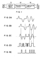
- a prior signal processing circuit based on the ⁇ V system is shown in Fig. 1, while signal waveforms at key points in this circuit are shown in Fig. 2.
- a read-out signal A from the magnetic head is delayed a predetermined time of period by analog delay circuit 61, which includes an LCR type filter.
- Signal A then becomes delayed signal B which, in turn, is differentiated by differentiator circuit 62.
- the resulting differentiated signal C is then supplied to comparator 63, where it is converted into a digital signal D.
- signal E corresponding to the write data is reproduced by use of digital signal D.
- an object of this invention is to provide a signal processing circuit based on the ⁇ V system, which can be assembled into an integrated circuit with a high packing density, and which can provide an easy circuit design.
- a signal processing circuit comprises differentiating means for differentiating an analog signal, means for converting the output signal from the differentiating means into a digital signal, and digital delay means for delaying the converted digital signal by a predetermined period of time.
- An analog signal input into the signal processing circuit is first differentiated, then digitized, and, finally, is delayed by the digital delay means.
- FIG. 3 A signal processing circuit according to an embodiment of this invention is shown in Fig. 3, with signal waveforms at key points in this circuit being shown in Fig. 4.
- a read-out signal a from the magnetic head is differentiated by differentiator circuit 11.
- the resulting differentiated signal b is supplied to differential type comparator 12, where it is converted into a digital signal c .
- signal d corresponding to the write data is reproduced using this digital signal d .
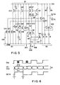
- Fig. 5 shows a detailed circuit diagram of a delay circuit used in the signal processing circuit described above.
- the signals input into this delay circuit i.e., the output signals from comparator 12, are complementary signals INA and INB.
- Signal INA is supplied to the base of NPN transistor Q1, and signal INB, to the base of NPN transistor Q2.
- Transistors Q1 and Q2 are interconnected at their emitters and form a differential amplifier 20 for amplifying signals INA and INB.
- capacitor C0 Located between and connected to the collectors of transistors Q1 and Q2 is capacitor C0. Differential amplifier 20 charges and discharges capacitor C0 according to the levels of input signals INA and INB.
- Bias voltage source VB1, resistor R1, NPN transistors Q3 and Q4, and NPN transistors Q5 to Q10 make up constant current source 30.
- Circuit 30 supplies a constant current I0 to the emitters of transistors Q1 and Q2, and a constant current I0/2 to transistors Q8 and Q9, the collectors of which are connected to the respective terminals of capacitor C0.
- the values of currents I0 and I0/2 can be adjusted by varying the resistance value of resistor R1.
- Clamp circuit 40 limits the voltage across capacitor C0 to the voltage drop ⁇ V across resistor R2, which is caused by constant current I2.
- Resistors R3 and R4, NPN transistors Q19 to Q22, and constant current sources I3 to I5 make up a differential type converter 50.
- Converter 50 amplifies the voltage across capacitor C0, waveshapes it, and produces complementary signals OUTA and OUTB. It should be noted that the circuit shown in Fig. 5, except for variable resistor R1 thereof, can entirely be formed in a form of an integrated circuit.
- the base of NPN transistor Q1 receives input signal INA, and the base of NPN transistor Q2 receives input signal INB.
- the collector of NPN transistor Q1 is connected to the collector of PNP transistor Q8, the emitter of which is connected to positive power supply Vcc.
- the collector of NPN transistor Q2 is connected to the collector of PNP transistor Q7, the emitter of which is connected to positive power supply Vcc.
- the emitter of NPN transistor Q1 is connected to the emitter of NPN transistor Q2.
- the node of the emitters of NPN transistors Q1 and Q2 is connected to the collector of NPN transistor Q3, the emitter of transistor Q3 being connected to the ground via variable resistor R1.
- the base of NPN transistor Q3 is connected to the base of NPN transistor Q4.
- the bases of NPN transistors Q3 and Q4 are connected to the positive polarity terminal of bias voltage supply VB1.
- the negative polarity terminal of bias voltage supply VB1 is connected to the ground.
- the emitter of NPN transistor Q4 is connected to the ground via variable resistor R1, and its collector is connected to the collector of PNP transistor Q5.
- the emitter of PNP transistor Q5 is connected to positive power supply Vcc.
- PNP transistor Q6 The base of PNP transistor Q6 is connected to the collector of NPN transistor Q4, its emitter is connected to the base of PNP transistor Q5, and its collector is connected to the ground.
- the collector of NPN transistor Q1 is also connected to the emitter of NPN transistor Q13, and the collector of NPN transistor Q2 is also connected to the emitter of NPN transistor Q12.
- the collectors of NPN transistors Q12 and Q13 are connected to positive power supply Vcc, the bases of transistors Q12 and Q13 being connected to the emitter of NPN transistors Q18.
- the collector of NPN transistor Q18 is connected to the ground.
- the emitter of NPN transistor Q18 is connected to the collector of PNP transistor Q9, the emitter of which is connected to positive power supply Vcc.
- the base of NPN transistor Q18 is connected to the ground via current source I2, as well as to the emitter of NPN transistor Q11, via resistor R2.
- the collector of NPN transistor Q11 is connected to positive power supply Vcc, and its base is connected to positive power supply Vcc via current source I1.
- the base of NPN transistor Q11 is also connected to the emitter of PNP transistor Q17.
- the collector of transistor Q17 is connected to the ground, and its base is connected to the collector of PNP transistor Q10, the emitter of which is connected to positive power supply Vcc.
- the collector of PNP transistor Q10 is also connected to the emitter of NPN transistor Q16, the collector of which is connected to the ground, and the base of which is connected to the positive terminal of bias voltage supply VB2 via the bases of NPN transistors Q14 and Q15.
- the negative terminal of bias voltage supply VB2 is connected to the ground.
- the collectors of NPN transistors Q14 and Q15 are connected to the ground.
- the emitter of NPN transistor Q14 is connected to the base of NPN transistor Q19, and the emitter of NPN transistor Q15 is connected to the gate of NPN transistor Q20.
- the collectors of NPN transistors Q19 and Q20 are connected to positive power supply Vcc.
- the emitter of NPN transistor Q19 is connected to the ground via current source I3, and the emitter of NPN transistor Q20 is connected to the ground via current source I4.
- the emitter of NPN transistor Q20 is also connected to the gates of NPN transistors Q21 and Q22.
- NPN transistor Q21 is connected to positive power supply Vcc via resistor R3
- the collector of NPN transistor Q22 is connected to positive power supply Vcc via resistor R4.
- the emitters of NPN transistors Q21 and Q22 are connected to the ground via common current source I5.
- the collector of NPN transistor Q22 forms an output terminal for outputting signal OUTA
- the collector of NPN transistor Q21 forms an output terminal for outputting signal OUTB.
- PNP transistors Q5, Q7, Q8, Q9, and Q10 are connected one another.
- Capacitor C0 is inserted between the collector of NPN transistor Q1 and the collector of NPN transistor Q2 and connected thereto.
- VC2 VB2 + VBE16 + VBE17 - VBE11 + ⁇ V + VBE18 - VBE12 ... (2) where VBE11, VBE12, VBE15, VBE16, VBE17, and VBE18 are respectively the base-emitter voltages of transistors Q11, Q12, and Q15 to Q18, and ⁇ V is the voltage drop across resistor R2, caused by constant current I2.
- the clamp voltage across capacitor C0 is determined by only the values of resistor R2 and constant current I2.
- Comparator 50 inverts the logical states of output signals OUTA and OUTB when the terminal voltages VC1 and VC2 of capacitor C0 coincide with each other.
- Capacitor C0 is charged by the current I0/2 during period T which starts when terminal voltages VC1 and VC2 change and which ends when those voltages are equal.
- the period T in the above equation (6) is the time delay of the output signal of the delay circuit to the input signals INA and INB, and is a function of I0 and ⁇ V.
- the time delay T can be kept constant. To set the time delay T to a desired value, it is only needed to use external resistor R1 of an appropriate resistance and constant current I0 of an appropriate current.
- a pulse delay circuit cannot delay the input signal exceeding its 1/2 pulse width of the input signal. Therefore, when the delay exceeding the 1/2 pulse width of the input signal is required for a particular use, a plurality of the delay circuits shown in Fig. 5 must be connected in cascade fashion.
- a signal processing circuit based on the ⁇ V system is provided, which can be built into the IC circuit and is simple in design.
Applications Claiming Priority (2)
| Application Number | Priority Date | Filing Date | Title |
|---|---|---|---|
| JP40025/87 | 1987-02-25 | ||
| JP62040025A JPH0775047B2 (ja) | 1987-02-25 | 1987-02-25 | 信号処理回路 |
Publications (3)
| Publication Number | Publication Date |
|---|---|
| EP0281009A2 true EP0281009A2 (de) | 1988-09-07 |
| EP0281009A3 EP0281009A3 (en) | 1989-06-14 |
| EP0281009B1 EP0281009B1 (de) | 1993-05-05 |
Family
ID=12569362
Family Applications (1)
| Application Number | Title | Priority Date | Filing Date |
|---|---|---|---|
| EP88102740A Expired - Lifetime EP0281009B1 (de) | 1987-02-25 | 1988-02-24 | Signal-Verarbeitungsschaltung |
Country Status (5)
| Country | Link |
|---|---|
| US (1) | US5081369A (de) |
| EP (1) | EP0281009B1 (de) |
| JP (1) | JPH0775047B2 (de) |
| KR (1) | KR910006569B1 (de) |
| DE (1) | DE3880713T2 (de) |
Families Citing this family (1)
| Publication number | Priority date | Publication date | Assignee | Title |
|---|---|---|---|---|
| US6208174B1 (en) * | 1999-12-14 | 2001-03-27 | Analog Devices, Inc. | High-speed comparator systems and methods with enhanced noise rejection |
Citations (4)
| Publication number | Priority date | Publication date | Assignee | Title |
|---|---|---|---|---|
| US3810232A (en) * | 1972-10-18 | 1974-05-07 | Singer Co | Magnetic memory read system for digital recordings |
| JPS58143412A (ja) * | 1982-02-18 | 1983-08-26 | Mitsubishi Electric Corp | 磁気記録装置の読取方式 |
| JPS61168106A (ja) * | 1985-01-18 | 1986-07-29 | Seiko Epson Corp | 磁気記録再生装置 |
| DE3604723A1 (de) * | 1985-03-22 | 1986-10-02 | Hitachi, Ltd., Tokio/Tokyo | Verfahren und vorrichtung zur optischen erfassung von informationen |
Family Cites Families (8)
| Publication number | Priority date | Publication date | Assignee | Title |
|---|---|---|---|---|
| JPS558051B2 (de) * | 1974-11-06 | 1980-03-01 | ||
| CA1086426A (en) * | 1975-10-13 | 1980-09-23 | Shunji Minami | Analog voltage memory device |
| US4091379A (en) * | 1976-05-03 | 1978-05-23 | Litton Business Systems, Inc. | Analog to digital wave shaping system |
| US4122490A (en) * | 1976-11-09 | 1978-10-24 | Lish Charles A | Digital chroma-key circuitry |
| US4183051A (en) * | 1977-07-01 | 1980-01-08 | Quadricolor Technology L.P. | Color television receiving system utilizing multimode inferred highs correction to reduce color infidelities |
| US4222008A (en) * | 1977-09-14 | 1980-09-09 | Rca Corporation | Apparatus for dividing an arbitrary waveform into equal-amplitude steps |
| JPS595410A (ja) * | 1982-06-22 | 1984-01-12 | ア−ルシ−エ− コ−ポレ−シヨン | デジタルデ−タ検知装置 |
| US4613973A (en) * | 1985-06-20 | 1986-09-23 | Eaton-Kenway, Inc. | Digital data decoder and method |
-
1987
- 1987-02-25 JP JP62040025A patent/JPH0775047B2/ja not_active Expired - Fee Related
-
1988
- 1988-02-24 EP EP88102740A patent/EP0281009B1/de not_active Expired - Lifetime
- 1988-02-24 KR KR1019880001885A patent/KR910006569B1/ko not_active IP Right Cessation
- 1988-02-24 DE DE8888102740T patent/DE3880713T2/de not_active Expired - Lifetime
-
1990
- 1990-06-27 US US07/545,139 patent/US5081369A/en not_active Expired - Lifetime
Patent Citations (4)
| Publication number | Priority date | Publication date | Assignee | Title |
|---|---|---|---|---|
| US3810232A (en) * | 1972-10-18 | 1974-05-07 | Singer Co | Magnetic memory read system for digital recordings |
| JPS58143412A (ja) * | 1982-02-18 | 1983-08-26 | Mitsubishi Electric Corp | 磁気記録装置の読取方式 |
| JPS61168106A (ja) * | 1985-01-18 | 1986-07-29 | Seiko Epson Corp | 磁気記録再生装置 |
| DE3604723A1 (de) * | 1985-03-22 | 1986-10-02 | Hitachi, Ltd., Tokio/Tokyo | Verfahren und vorrichtung zur optischen erfassung von informationen |
Non-Patent Citations (3)
| Title |
|---|
| IEEE TRANSACTIONS ON COMPUTERS, vol. C-17, no. 9, September 1968, pages 827-845, New York, US; T.H. CHEN: "The use of delay lines in reading a Manchester code" * |
| PATENT ABSTRACTS OF JAPAN, vol. 10, no. 374 (P-527)[2431], 12th December 1986; & JP-A-61 168 106 (SEIKO EPSON CORP.) 29-07-1986 * |
| PATENT ABSTRACTS OF JAPAN, vol. 7, no. 262 (P-238)[1407], 22nd November 1983; & JP-A-58 143 412 (MITSUBISHU DENKI K.K.) 26-08-1983 * |
Also Published As
| Publication number | Publication date |
|---|---|
| KR880010381A (ko) | 1988-10-08 |
| DE3880713T2 (de) | 1993-08-19 |
| KR910006569B1 (ko) | 1991-08-28 |
| JPS63209006A (ja) | 1988-08-30 |
| DE3880713D1 (de) | 1993-06-09 |
| JPH0775047B2 (ja) | 1995-08-09 |
| EP0281009A3 (en) | 1989-06-14 |
| EP0281009B1 (de) | 1993-05-05 |
| US5081369A (en) | 1992-01-14 |
Similar Documents
| Publication | Publication Date | Title |
|---|---|---|
| US4773096A (en) | Digital switching power amplifier | |
| US5592097A (en) | Load open state detection using H-bridge driving circuit | |
| EP0108812A1 (de) | Analog/digital umwandler | |
| EP1385174A1 (de) | Schnelle Abtast- und Halte Spitzenwerkdetektorschaltung | |
| US4667118A (en) | Monostable multivibrator | |
| EP0281009A2 (de) | Signal-Verarbeitungsschaltung | |
| JP2992584B2 (ja) | パルス検出回路 | |
| JPH0356486B2 (de) | ||
| US4636659A (en) | Sample and hold circuit | |
| US3444473A (en) | Fast recovery read amplifier | |
| US5315449A (en) | Time code signal processing circuit for removing and restoring variation in slew rate | |
| JPH07169004A (ja) | プリアンプ回路装置 | |
| US5543976A (en) | Providing transitions of slew rate dependent on pulse frequency | |
| EP0279993B1 (de) | Unterdrückungsschaltung von unerwünschten zeitlichen Abschnitten eines variablen Spannungssignals | |
| US4845573A (en) | System with filter system for improved reliability for recording data on a magnetic recording medium | |
| JP3073619B2 (ja) | サンプルホールド回路 | |
| JPH0773179B2 (ja) | 微分回路 | |
| KR101020244B1 (ko) | D/a변환 인터페이스 | |
| GB917750A (en) | System for reading magnetically recorded information signals | |
| KR0182968B1 (ko) | 하드디스크 드라이버의 플립플롭 버퍼회로 | |
| JP3111559B2 (ja) | 磁気ヘッド断線検出回路 | |
| SU1413669A1 (ru) | Устройство дл формировани воспроизводимых с магнитного носител бинарных сигналов | |
| KR100492984B1 (ko) | 영상 신호의 고주파 증강 제어장치 | |
| JPS63222515A (ja) | スイツチ回路 | |
| JPS6219106B2 (de) |
Legal Events
| Date | Code | Title | Description |
|---|---|---|---|
| PUAI | Public reference made under article 153(3) epc to a published international application that has entered the european phase |
Free format text: ORIGINAL CODE: 0009012 |
|
| 17P | Request for examination filed |
Effective date: 19880321 |
|
| AK | Designated contracting states |
Kind code of ref document: A2 Designated state(s): DE FR GB |
|
| PUAL | Search report despatched |
Free format text: ORIGINAL CODE: 0009013 |
|
| AK | Designated contracting states |
Kind code of ref document: A3 Designated state(s): DE FR GB |
|
| 17Q | First examination report despatched |
Effective date: 19910131 |
|
| GRAA | (expected) grant |
Free format text: ORIGINAL CODE: 0009210 |
|
| AK | Designated contracting states |
Kind code of ref document: B1 Designated state(s): DE FR GB |
|
| REF | Corresponds to: |
Ref document number: 3880713 Country of ref document: DE Date of ref document: 19930609 |
|
| ET | Fr: translation filed | ||
| PLBE | No opposition filed within time limit |
Free format text: ORIGINAL CODE: 0009261 |
|
| STAA | Information on the status of an ep patent application or granted ep patent |
Free format text: STATUS: NO OPPOSITION FILED WITHIN TIME LIMIT |
|
| 26N | No opposition filed | ||
| PGFP | Annual fee paid to national office [announced via postgrant information from national office to epo] |
Ref country code: FR Payment date: 19970211 Year of fee payment: 10 |
|
| PGFP | Annual fee paid to national office [announced via postgrant information from national office to epo] |
Ref country code: GB Payment date: 19970217 Year of fee payment: 10 |
|
| PG25 | Lapsed in a contracting state [announced via postgrant information from national office to epo] |
Ref country code: GB Free format text: LAPSE BECAUSE OF NON-PAYMENT OF DUE FEES Effective date: 19980224 |
|
| PG25 | Lapsed in a contracting state [announced via postgrant information from national office to epo] |
Ref country code: FR Free format text: THE PATENT HAS BEEN ANNULLED BY A DECISION OF A NATIONAL AUTHORITY Effective date: 19980228 |
|
| GBPC | Gb: european patent ceased through non-payment of renewal fee |
Effective date: 19980224 |
|
| REG | Reference to a national code |
Ref country code: FR Ref legal event code: ST |
|
| PGFP | Annual fee paid to national office [announced via postgrant information from national office to epo] |
Ref country code: DE Payment date: 20070222 Year of fee payment: 20 |