EP0267553B1 - Circuit numérique de verrouillage et de gain - Google Patents
Circuit numérique de verrouillage et de gain Download PDFInfo
- Publication number
- EP0267553B1 EP0267553B1 EP87116413A EP87116413A EP0267553B1 EP 0267553 B1 EP0267553 B1 EP 0267553B1 EP 87116413 A EP87116413 A EP 87116413A EP 87116413 A EP87116413 A EP 87116413A EP 0267553 B1 EP0267553 B1 EP 0267553B1
- Authority
- EP
- European Patent Office
- Prior art keywords
- waveform
- gain
- output
- clip
- input
- Prior art date
- Legal status (The legal status is an assumption and is not a legal conclusion. Google has not performed a legal analysis and makes no representation as to the accuracy of the status listed.)
- Expired - Lifetime
Links
Images
Classifications
-
- H—ELECTRICITY
- H04—ELECTRIC COMMUNICATION TECHNIQUE
- H04N—PICTORIAL COMMUNICATION, e.g. TELEVISION
- H04N5/00—Details of television systems
- H04N5/222—Studio circuitry; Studio devices; Studio equipment
- H04N5/262—Studio circuits, e.g. for mixing, switching-over, change of character of image, other special effects ; Cameras specially adapted for the electronic generation of special effects
- H04N5/265—Mixing
-
- H—ELECTRICITY
- H04—ELECTRIC COMMUNICATION TECHNIQUE
- H04N—PICTORIAL COMMUNICATION, e.g. TELEVISION
- H04N5/00—Details of television systems
- H04N5/14—Picture signal circuitry for video frequency region
- H04N5/20—Circuitry for controlling amplitude response
Definitions
- the present invention relates to clip and gain circuits, and more particularly to a digital clip and gain circuit for generating a new control waveform from an input waveform.
- a digital chroma key generator which includes a clip and gain circuit comprising a subtracter at whose output there appears the difference between an input waveform and a clip level, this difference signal being fed after processing to an amplifying means for amplifying the difference waveform by a gain value.
- the circuit disclosed in this document forms the preamble to claim 1.
- clip and gain circuits are used for video processing where an input waveform is compared with a reference level and the difference value is amplified, level shifted and limited to generate a control waveform.
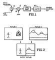
- a typical clip and gain circuit known to the applicants is shown in Fig. 1.
- Typical examples of applications for clip and gain circuits are "wipe", “self-key” and “depth” effects.
- a wipe is a method by which two video pictures are combined into one output picture by spatially dividing the output into two or more separate spaces, each of which contains the corresponding video from one of the inputs.
- Fig. 2 shows a simple "split-screen" wipe, where the left side of the output picture consists of the left side of a first input and the right side of the output picture consists of the right side of a second input.
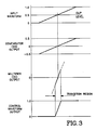
- This effect is accomplished by first generating a ramp waveform which is a low voltage in areas corresponding to the left side of the picture and a high voltage in areas corresponding to the right side of the picture, as illustrated in Fig. 3.
- This waveform becomes the input to the clip and gain circuit where it is compared with a reference, or clip, voltage and the difference value is amplified.
- the resulting output may be used to drive the control input of a mixer whose two inputs are the two pictures.
- the output of the comparator In areas where the ramp waveform is much lower than the clip voltage, the output of the comparator, or subtracter, is negative. The negative output is amplified and converted to a control voltage which enables the mixer to turn on the first picture's video. Conversely, where the ramp waveform is much higher than the clip voltage, the output of the comparator is positive. The positive output is similarly converted to a control voltage which enables the mixer to turn on the second picture's video.
- the output of the comparator When the ramp waveform is close in level to the clip voltage, the output of the comparator is close to zero which, depending upon the gain of the amplifier, may not result in an output level that fully drives the mixer fully to either limit, i.e., the mixer outputs some proportional mix of the two input pictures.
- This proportional mixing which occurs at the boundaries between two pictures, is called “softness” and provides for a graceful transition from one picture to another.
- the width of the softness region depends on the gain of the amplifier and the slope of the ramp waveform. By providing operator control over the gain and clip settings the transition region may be moved left to right in space and its width may be varied.
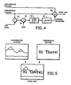
- one of the two inputs to the mixer is also an input to the comparator, as shown in Fig. 4.
- the resulting control waveform causes the mixer to output the first picture
- the resulting control waveform causes the mixer to output the second picture.
- bright, or high level areas of the second picture take priority over the first picture's video
- dark, or low level areas of the second picture are subordinated to the first picture. If the second picture is lettering on a dark background as shown in Fig. 5, then the resulting picture is those letters over the first picture.
- the input waveform is a signal whose voltage is proportional to the second picture's depth, or apparent distance from the viewer in the picture, or an object in the picture.
- the second picture is made to "disappear” into the first picture.
- the clip voltage represents a depth beyond which the viewer could not see the second picture.
- the major design obstacle is noise, since any noise appearing on the input waveform near the clip voltage is amplified and causes false or uneven mixing between the two pictures at the transition point.
- random noise is less of a problem, especially if the input waveform has been digitally generated, but the input waveform must generally be represented by many bits to avoid similar effects due to quantization noise.
- a gain large enough to make the desired small transition region uses up all of the bits and the output of the control waveform to the mixer jumps from the off, picture one, level to the on, picture two, level without any intervening steps. On diagonal edges this causes the transition to look "jaggy", or stair-stepped, instead of a more pleasing fade from one picture to the other.
- this distortion becomes less pronounced, but the cost of the clip and gain circuit rises due to the complexity and cost of a larger multiplier.
- a typical clip and gain circuit has gain values as low as 0.00, circuit off, and as high as 512.0 to 1024.0. Additionally the fractional precision needed at small gains is high, often eight or more bits, to avoid "cogging", or a noticeable jump in transition width as the gain is smoothly varied. The combined number of bits required for the range and fraction precision of the gain values also makes the circuit more costly and complex. This is particularly true of the gain multiplier since the number of bits required at the output of the multiplier is the sum of the number of bits at the two inputs.
- the input waveform may need as many as twenty bits, which becomes twenty-one after the comparator, and the gain value may need as many as eighteen bits for an output precision of thirty-eight bits.
- a typical mixer control waveform is only ten bits, but the full thirty-eight bits must be generated to insure that over range values are properly limit detected and clipped.
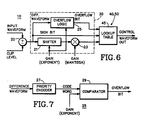
- a digital clip and gain circuit having comparison means for comparing a input waveform with a reference (CLIP) level to produce a difference waveform, and amplifying means for amplifying the difference waveform by a gain value, the input waveform, reference level and difference waveform being digital values characterized in that:- said amplifying means comprises shifting means for digitally shifting said difference waveform according to an exponent portion of the gain value representing a power of two value of the gain value, and means for multiplying the output from the shifting means by a mantissa portion of the gain value representing a fractional portion of the gain value, and further characterized by level shifting and limiting means for level shifting and limiting the amplified difference waveform to produce a control waveform.
- CLIP reference
- the present invention provides a digital clip and gain circuit which treats the gain multiplication in two steps.
- the output of a comparator which performs the comparison of an input waveform with a clip level is input into a gain stage having two parts, an exponent shifter followed by a mantissa multiplier.
- the exponent shifter shifts the comparator output by some number of bits and the mantissa multiplier performs a multiplication within the range of 0.0 to just less than 2.0.
- the desired gain value is input as a desired power of two multiple to the exponent shifter and as a fractional gain portion to the mantissa multiplier.
- the output of the comparator is also input to an overflow logic circuit to test for input values which will be over limit after gain multiplication.
- the output of the mantissa multiplier, the sign bit from the comparator and the output of the overflow logic circuit are input to a lookup table which provides level shifting and limiting of the mantissa multiplier output to produce a new control waveform.
- Fig. 1 is a general block diagram of a clip and gain circuit.
- Fig. 2 is a pictorial illustration of a wipe effect.
- Fig. 3 is a waveform diagram illustrating the operation of a clip and gain circuit.
- Fig. 4 is a general block diagram of a clip and gain circuit used to produce a self-key effect.
- Fig. 5 is a pictorial illustration of a self-key effect.
- Fig. 6 is a detailed block diagram of the clip and gain circuit of Fig. 1 according to the present invention.
- Fig. 7 is a block diagram of the overflow logic for the clip and gain circuit of Fig. 6 according to the present invention.
- an input waveform and a clip level are input to a comparator 20.
- the output of the comparator 20 is a difference waveform which is negative where the input waveform is less than the clip level and positive where the input waveform is greater than the clip level.
- the difference waveform is input to a multiplier, or gain, stage 30.
- the output of the gain stage 30 is input to a level shifter 40, the output of which is input to a limiter 50 to produce a new control waveform at the output.
- the control waveform is subsequently input to a mixer 60 where two video pictures are combined as determined by the control waveform.
- the clip and gain circuit is digital to eliminate the analog noise problems where the input waveform is close in value to the clip level.
- the input waveform is twenty bits
- the output of the comparator 20 is twenty bits plus a sign bit for a total of twenty-one bits.
- the difference waveform is input to a shifter 21 in the gain stage 30.
- the gain value is divided into an exponent gain value which is a multiple of two and a mantissa gain value which is the fractional portion of the gain value.
- the exponent gain value is input to the shifter 21 to shift the difference waveform accordingly, corresponding to multiplying the difference waveform by a power of two.
- the output of the shifter 21 is then input to a multiplier 23 where it is multiplied by the mantissa gain value which has a value between 0.0 and just less than 2.0.
- the resulting output from the multiplier 23 together with the sign bit from the comparator 21 are input to a lookup table 45 which provides the level shifting and limiting functions to produce the new control waveform at the output.
- the difference waveform is also input to an overflow logic circuit 25.
- the difference waveform is combined with the exponent gain value to determine if the result of the multiplication by the gain stage 30 will produce an out of limits result.
- An overflow bit is set if the multiplication would produce such an out of limits value.
- the overflow bit is input to the lookup table 45 together with the sign bit and the output of the lookup table is set to either the maximum or minimum value according to the sign bit, overriding the output of the multiplier 23.
- the overflow logic circuit 25 has a priority encoder 27 to which the difference waveform is input.
- the priority encoder 27 determines the position of the most significant bit (MSB) of the difference waveform and develops a code word accordingly.
- MSB most significant bit
- the code word from the priority encoder 27, which is preferably a PROM lookup table, is input to an overflow comparator 29 to which is also input the exponent gain value. If the comparison of the code word with the exponent gain value indicates an overflow condition, the overflow bit from the overflow comparator 29 is set indicating that the difference waveform is out of range, and the lookup table 45 uses the sign bit together with the overflow bit to output the maximum (+) or minimum (-) mixer control waveform. If the overflow bit is not set, the lookup table 45 translates the output of the multiplier 23 along with the sign bit into the desired output.
- the desired gain value is input to the clip and gain circuit 10 in a normalized floating point form, and is split into an exponent gain value and a mantissa gain value by either software at the input interface or by a hardware lookup table.
- Table I illustrates some typical gain values and the conversion into exponent and mantissa gain values: The exponent and mantissa values each start at zero for a gain of zero. As the gain increases the mantissa value follows until the gain equals two, at which point the exponent increases to one and the mantissa drops back to 1.00. The mantissa then continues to increase with rising gain until the gain is 4.00, when the exponent increases to 2 and the mantissa again drops back to 1.00.
- the multiplier 23 in the gain stage 30 also is much smaller in the number of bits handled than the conventional design because the present invention only provides the full fractional gain accuracy when necessary -- at low gains. Further the output of the multiplier 23 is only the number of bits needed for the mixer control waveform since overflow detection is handled as a separate circuit. Finally the output precision and gain are well constrained since the input from the shifter 21 is only those bits needed to generate the desired mixer control waveform accuracy, not the entire difference waveform precision.
- lookup table 45 performs the level shifting and limiting functions, these functions could also be done in separate lookup tables or processed by separate special purpose circuits. Also the lookup table 45 may be used to apply waveform shaping to the mixer control waveform, such as S-shaping to prevent abrupt transitions at the limit points to reduce the appearance of "Mach bands", or transition derivative discontinuities, in the final video output.
- waveform shaping such as S-shaping to prevent abrupt transitions at the limit points to reduce the appearance of "Mach bands", or transition derivative discontinuities, in the final video output.
- the present invention provides a digital clip and gain circuit which is simpler and less costly by reducing the size of the multiplier.
- the gain multiplication is treated in two steps: an exponent shift and a mantissa multiply.
- parallel overflow logic is used to avoid the need for a wide dynamic range multiplier.
Landscapes
- Engineering & Computer Science (AREA)
- Multimedia (AREA)
- Signal Processing (AREA)
- Studio Circuits (AREA)
- Tone Control, Compression And Expansion, Limiting Amplitude (AREA)
- Control Of Amplification And Gain Control (AREA)
- Analogue/Digital Conversion (AREA)
- Electrophonic Musical Instruments (AREA)
Claims (3)
- Circuit numérique de coupure et d'amplification comportant des moyens de comparaison (20) pour comparer une forme d'onde d'entrée à un niveau de référence (COUPURE) afin de produire une forme d'onde de différence, et des moyens d'amplification (30) pour amplifier la forme d'onde de différence d'un coefficient d'amplification ou valeur de gain, la forme d'onde d'entrée, le niveau de référence et la forme d'onde de différence étant des valeurs numériques, caractérisé en ce que :
lesdits moyens d'amplification comprennent des moyens de décalage (21) pour décaler numériquement ladite forme d'onde de différence conformément à une partie exposant de la valeur de gain, qui représente une valeur de puissance de deux de la valeur de gain, et des moyens (23) de multiplication de la sortie des moyens de décalage par une partie mantisse de la valeur de gain, qui représente une partie fractionnelle de la valeur de gain, et caractérisé en outre par des moyens de décalage de niveau et de limitation (40,50) pour décaler le niveau et limiter la forme d'onde de différence amplifiée afin de produire une forme d'onde de commande. - Circuit numérique de coupure et d'amplification suivant la revendication 1, dans lequel les moyens d'amplification comprennent en outre des moyens de détermination (25) pour déterminer, à partir de la forme d'onde de différence et de la partie exposant de la valeur de gain, une situation de débordement indiquant que la sortie des moyens de multiplication est en dehors de limites prédéterminées.
- Circuit numérique de coupure et d'amplification suivant la revendication 2, dans lequel les moyens de décalage de niveau et de limitation comprennent une table de consultation (45) ayant comme entrées la sortie des moyens de multiplication, un bit de signe provenant de la forme d'onde de différence et un bit de débordement provenant des moyens de détermination et représentant l'état de débordement, la table de consultation fournissant une valeur maximale ou minimale prédéterminée pour la forme d'onde de commande qui dépend du bit de signe lorsque le bit de débordement indique l'état de débordement, et fournissant une valeur pour la forme d'onde de commande qui représente la sortie des moyens de multiplication et le bit de signe lorsque le bit de débordement indique qu'il n'y a pas d'état de débordement.
Applications Claiming Priority (2)
| Application Number | Priority Date | Filing Date | Title |
|---|---|---|---|
| US931382 | 1986-11-14 | ||
| US06/931,382 US4771192A (en) | 1986-11-14 | 1986-11-14 | Digital clip and gain circuit |
Publications (3)
| Publication Number | Publication Date |
|---|---|
| EP0267553A2 EP0267553A2 (fr) | 1988-05-18 |
| EP0267553A3 EP0267553A3 (fr) | 1991-02-06 |
| EP0267553B1 true EP0267553B1 (fr) | 1993-08-04 |
Family
ID=25460704
Family Applications (1)
| Application Number | Title | Priority Date | Filing Date |
|---|---|---|---|
| EP87116413A Expired - Lifetime EP0267553B1 (fr) | 1986-11-14 | 1987-11-06 | Circuit numérique de verrouillage et de gain |
Country Status (6)
| Country | Link |
|---|---|
| US (1) | US4771192A (fr) |
| EP (1) | EP0267553B1 (fr) |
| JP (1) | JPH0771221B2 (fr) |
| AU (1) | AU592904B2 (fr) |
| CA (1) | CA1264491A (fr) |
| DE (1) | DE3786881T2 (fr) |
Cited By (2)
| Publication number | Priority date | Publication date | Assignee | Title |
|---|---|---|---|---|
| US6141063A (en) * | 1996-09-25 | 2000-10-31 | U.S. Philips Corporation | Chroma key method and arrangement |
| DE102009020867B4 (de) | 2009-05-12 | 2022-01-27 | Bayerische Motoren Werke Aktiengesellschaft | Brennkraftmaschine mit einem Kraftstoffinjektor |
Families Citing this family (20)
| Publication number | Priority date | Publication date | Assignee | Title |
|---|---|---|---|---|
| US4823183A (en) * | 1988-02-01 | 1989-04-18 | The Grass Valley Group, Inc. | Video mixer with multicolor boarder |
| US4805022A (en) * | 1988-02-19 | 1989-02-14 | The Grass Valley Group, Inc. | Digital wipe generator |
| US4873568A (en) * | 1988-09-19 | 1989-10-10 | The Grass Valley Group, Inc. | Digital video effects apparatus |
| US4949177A (en) * | 1988-09-19 | 1990-08-14 | The Grass Valley Group, Inc. | Method and apparatus for carrying out a non-linear operation on a digital signal |
| US4947255A (en) * | 1988-09-19 | 1990-08-07 | The Grass Valley Group, Inc. | Video luminance self keyer |
| US4920415A (en) * | 1989-03-20 | 1990-04-24 | The Grass Valley Group, Inc. | Self keyer |
| DE3932757C2 (de) * | 1989-09-30 | 1998-07-23 | Philips Broadcast Television S | Verfahren und Anordnung zur Ableitung eines Stanzsignals |
| US5258928A (en) * | 1990-05-03 | 1993-11-02 | Rca Thomson Licensing Corporation | Parts efficient memory based functional circuit having selectable transfer characteristics |
| KR920008630B1 (ko) * | 1990-09-28 | 1992-10-02 | 삼성전자 주식회사 | 수평윤곽 보상회로 |
| KR0168404B1 (ko) * | 1990-12-06 | 1999-03-20 | 오오가 노리오 | 피드백 클램프 회로 |
| US5315537A (en) * | 1991-04-08 | 1994-05-24 | Blacker Teddy D | Automated quadrilateral surface discretization method and apparatus usable to generate mesh in a finite element analysis system |
| EP0518465B1 (fr) * | 1991-06-14 | 1999-06-16 | The Grass Valley Group, Inc. | Mélangeur vidéo |
| JP3016652B2 (ja) * | 1992-02-07 | 2000-03-06 | 松下電器産業株式会社 | ゲインコントロール回路 |
| JPH06292077A (ja) * | 1993-03-30 | 1994-10-18 | Sony Corp | 特殊効果装置 |
| JP3503166B2 (ja) * | 1993-07-29 | 2004-03-02 | ソニー株式会社 | 信号変換装置および方法 |
| GB2282293B (en) * | 1993-09-10 | 1997-08-27 | Sony Uk Ltd | A method of and apparatus for deriving a key signal from a digital video signal |
| US6456300B1 (en) * | 1999-03-31 | 2002-09-24 | Autodesk Canada Inc. | Method and apparatus for processing image data to produce control data |
| JP3663973B2 (ja) * | 1999-05-06 | 2005-06-22 | 日本電気株式会社 | 画像信号処理装置および画像信号処理方法 |
| JP4662737B2 (ja) * | 2004-06-17 | 2011-03-30 | セイコーNpc株式会社 | アッテネータ、アッテネータの減衰量取得方法及びプログラム |
| US7800402B1 (en) * | 2007-11-05 | 2010-09-21 | Altera Corporation | Look-up table overdrive circuits |
Family Cites Families (8)
| Publication number | Priority date | Publication date | Assignee | Title |
|---|---|---|---|---|
| US3619495A (en) * | 1969-08-21 | 1971-11-09 | Nippon Electric Co | Television picture montage circuit |
| US3673324A (en) * | 1969-12-23 | 1972-06-27 | Tokyo Broadcasting Syst | Video mixing/special effects amplifiers |
| US3736377A (en) * | 1971-05-10 | 1973-05-29 | R Warren | Multiple channel video switching system |
| JPS52139343A (en) * | 1976-05-17 | 1977-11-21 | Hitachi Ltd | Agc circuit |
| US4356511A (en) * | 1978-05-23 | 1982-10-26 | Sony Corporation | Digital soft-edge video special effects generator |
| US4386363A (en) * | 1981-04-10 | 1983-05-31 | Ampex Corporation | Chroma key switching signal generator |
| US4392156A (en) * | 1981-05-04 | 1983-07-05 | Ampex Corporation | Video key edge generator for increasing the size of an associated border, drop shadow and/or outline |
| JPS58151179A (ja) * | 1982-03-03 | 1983-09-08 | Matsushita Electric Ind Co Ltd | ワイプキ−信号発生回路 |
-
1986
- 1986-11-14 US US06/931,382 patent/US4771192A/en not_active Expired - Lifetime
-
1987
- 1987-11-06 EP EP87116413A patent/EP0267553B1/fr not_active Expired - Lifetime
- 1987-11-06 DE DE87116413T patent/DE3786881T2/de not_active Expired - Fee Related
- 1987-11-12 JP JP62286434A patent/JPH0771221B2/ja not_active Expired - Lifetime
- 1987-11-12 CA CA000551629A patent/CA1264491A/fr not_active Expired - Fee Related
- 1987-11-13 AU AU81190/87A patent/AU592904B2/en not_active Ceased
Cited By (3)
| Publication number | Priority date | Publication date | Assignee | Title |
|---|---|---|---|---|
| US6141063A (en) * | 1996-09-25 | 2000-10-31 | U.S. Philips Corporation | Chroma key method and arrangement |
| DE19639355B4 (de) * | 1996-09-25 | 2006-05-04 | Bts Holding International Bv | Verfahren und Anordnung zum Farbstanzen |
| DE102009020867B4 (de) | 2009-05-12 | 2022-01-27 | Bayerische Motoren Werke Aktiengesellschaft | Brennkraftmaschine mit einem Kraftstoffinjektor |
Also Published As
| Publication number | Publication date |
|---|---|
| JPH0771221B2 (ja) | 1995-07-31 |
| AU592904B2 (en) | 1990-01-25 |
| EP0267553A3 (fr) | 1991-02-06 |
| DE3786881T2 (de) | 1994-02-24 |
| DE3786881D1 (de) | 1993-09-09 |
| JPS63211881A (ja) | 1988-09-02 |
| CA1264491A (fr) | 1990-01-16 |
| AU8119087A (en) | 1988-05-19 |
| US4771192A (en) | 1988-09-13 |
| EP0267553A2 (fr) | 1988-05-18 |
Similar Documents
| Publication | Publication Date | Title |
|---|---|---|
| EP0267553B1 (fr) | Circuit numérique de verrouillage et de gain | |
| US7222037B2 (en) | Hybrid automatic gain control (AGC) | |
| US5638138A (en) | Method for electronic image dynamic range and contrast modification | |
| EP0630160A2 (fr) | Contrôle dynamique du contraste par la correction | |
| US7050114B2 (en) | Picture signal contrast control | |
| EP0360518B1 (fr) | Dispositif de déclenchement inhérent de luminance de vidéo | |
| US4935806A (en) | Chroma noise reduction and transient improvement | |
| WO2002037835A2 (fr) | Prevention adaptative de l'ecretage permettant d'ameliorer la nettete d'image | |
| EP0217938B1 (fr) | Appareil et procede de traitement de signaux video prealablement traites | |
| EP0506380A2 (fr) | Appareil de traitement d'images | |
| US7742190B2 (en) | Image processing method and apparatus | |
| EP0335371A2 (fr) | Filtre numérique pour exécuter un proccessus d'accentuation de l'image au moyen de sélection de mode | |
| EP0475725B1 (fr) | Amélioration d'image | |
| JP2727033B2 (ja) | キー装置 | |
| US5142365A (en) | Circuit for controlling contrast in a digital television receiver | |
| GB2282293A (en) | Deriving a key signal from a digital video signal | |
| KR100398979B1 (ko) | 비디오신호를처리하기위한장치및방법 | |
| US7791759B2 (en) | Image processing method and apparatus | |
| JP2752810B2 (ja) | 輪郭修整回路 | |
| JP2004312160A (ja) | 映像信号処理回路 | |
| EP1262941A1 (fr) | Méthode de mise en oeuvre de traitement d'images par diffusion des erreurs pour un panneau d'affichage à plasma | |
| JPH08279912A (ja) | 輪郭補正方法及び輪郭補正回路 | |
| KR980013454A (ko) | 루미넌스 변화에 따른 칼라 보상 방법 및 그 회로(thereof) | |
| JPH01259674A (ja) | 高域強調回路 |
Legal Events
| Date | Code | Title | Description |
|---|---|---|---|
| PUAI | Public reference made under article 153(3) epc to a published international application that has entered the european phase |
Free format text: ORIGINAL CODE: 0009012 |
|
| AK | Designated contracting states |
Kind code of ref document: A2 Designated state(s): DE FR GB |
|
| PUAL | Search report despatched |
Free format text: ORIGINAL CODE: 0009013 |
|
| RHK1 | Main classification (correction) |
Ipc: H04N 5/20 |
|
| AK | Designated contracting states |
Kind code of ref document: A3 Designated state(s): DE FR GB |
|
| 17P | Request for examination filed |
Effective date: 19910208 |
|
| 17Q | First examination report despatched |
Effective date: 19920716 |
|
| GRAA | (expected) grant |
Free format text: ORIGINAL CODE: 0009210 |
|
| AK | Designated contracting states |
Kind code of ref document: B1 Designated state(s): DE FR GB |
|
| PG25 | Lapsed in a contracting state [announced via postgrant information from national office to epo] |
Ref country code: FR Effective date: 19930804 |
|
| REF | Corresponds to: |
Ref document number: 3786881 Country of ref document: DE Date of ref document: 19930909 |
|
| PGFP | Annual fee paid to national office [announced via postgrant information from national office to epo] |
Ref country code: FR Payment date: 19931011 Year of fee payment: 7 |
|
| EN | Fr: translation not filed | ||
| PLBE | No opposition filed within time limit |
Free format text: ORIGINAL CODE: 0009261 |
|
| STAA | Information on the status of an ep patent application or granted ep patent |
Free format text: STATUS: NO OPPOSITION FILED WITHIN TIME LIMIT |
|
| 26N | No opposition filed | ||
| PGFP | Annual fee paid to national office [announced via postgrant information from national office to epo] |
Ref country code: DE Payment date: 19981027 Year of fee payment: 12 |
|
| PG25 | Lapsed in a contracting state [announced via postgrant information from national office to epo] |
Ref country code: DE Free format text: LAPSE BECAUSE OF NON-PAYMENT OF DUE FEES Effective date: 20000901 |
|
| REG | Reference to a national code |
Ref country code: GB Ref legal event code: IF02 |
|
| PGFP | Annual fee paid to national office [announced via postgrant information from national office to epo] |
Ref country code: GB Payment date: 20050926 Year of fee payment: 19 |
|
| GBPC | Gb: european patent ceased through non-payment of renewal fee |
Effective date: 20061106 |
|
| PG25 | Lapsed in a contracting state [announced via postgrant information from national office to epo] |
Ref country code: GB Free format text: LAPSE BECAUSE OF NON-PAYMENT OF DUE FEES Effective date: 20061106 |