EP0264918B1 - Bildanzeigevorrichtung - Google Patents
Bildanzeigevorrichtung Download PDFInfo
- Publication number
- EP0264918B1 EP0264918B1 EP87115354A EP87115354A EP0264918B1 EP 0264918 B1 EP0264918 B1 EP 0264918B1 EP 87115354 A EP87115354 A EP 87115354A EP 87115354 A EP87115354 A EP 87115354A EP 0264918 B1 EP0264918 B1 EP 0264918B1
- Authority
- EP
- European Patent Office
- Prior art keywords
- signals
- single pixel
- converter
- electrodes
- remaining
- Prior art date
- Legal status (The legal status is an assumption and is not a legal conclusion. Google has not performed a legal analysis and makes no representation as to the accuracy of the status listed.)
- Expired - Lifetime
Links
Images


Classifications
-
- H—ELECTRICITY
- H04—ELECTRIC COMMUNICATION TECHNIQUE
- H04N—PICTORIAL COMMUNICATION, e.g. TELEVISION
- H04N5/00—Details of television systems
- H04N5/44—Receiver circuitry for the reception of television signals according to analogue transmission standards
-
- G—PHYSICS
- G09—EDUCATION; CRYPTOGRAPHY; DISPLAY; ADVERTISING; SEALS
- G09G—ARRANGEMENTS OR CIRCUITS FOR CONTROL OF INDICATING DEVICES USING STATIC MEANS TO PRESENT VARIABLE INFORMATION
- G09G3/00—Control arrangements or circuits, of interest only in connection with visual indicators other than cathode-ray tubes
- G09G3/20—Control arrangements or circuits, of interest only in connection with visual indicators other than cathode-ray tubes for presentation of an assembly of a number of characters, e.g. a page, by composing the assembly by combination of individual elements arranged in a matrix no fixed position being assigned to or needed to be assigned to the individual characters or partial characters
- G09G3/34—Control arrangements or circuits, of interest only in connection with visual indicators other than cathode-ray tubes for presentation of an assembly of a number of characters, e.g. a page, by composing the assembly by combination of individual elements arranged in a matrix no fixed position being assigned to or needed to be assigned to the individual characters or partial characters by control of light from an independent source
- G09G3/36—Control arrangements or circuits, of interest only in connection with visual indicators other than cathode-ray tubes for presentation of an assembly of a number of characters, e.g. a page, by composing the assembly by combination of individual elements arranged in a matrix no fixed position being assigned to or needed to be assigned to the individual characters or partial characters by control of light from an independent source using liquid crystals
- G09G3/3607—Control arrangements or circuits, of interest only in connection with visual indicators other than cathode-ray tubes for presentation of an assembly of a number of characters, e.g. a page, by composing the assembly by combination of individual elements arranged in a matrix no fixed position being assigned to or needed to be assigned to the individual characters or partial characters by control of light from an independent source using liquid crystals for displaying colours or for displaying grey scales with a specific pixel layout, e.g. using sub-pixels
-
- G—PHYSICS
- G09—EDUCATION; CRYPTOGRAPHY; DISPLAY; ADVERTISING; SEALS
- G09G—ARRANGEMENTS OR CIRCUITS FOR CONTROL OF INDICATING DEVICES USING STATIC MEANS TO PRESENT VARIABLE INFORMATION
- G09G3/00—Control arrangements or circuits, of interest only in connection with visual indicators other than cathode-ray tubes
- G09G3/20—Control arrangements or circuits, of interest only in connection with visual indicators other than cathode-ray tubes for presentation of an assembly of a number of characters, e.g. a page, by composing the assembly by combination of individual elements arranged in a matrix no fixed position being assigned to or needed to be assigned to the individual characters or partial characters
- G09G3/34—Control arrangements or circuits, of interest only in connection with visual indicators other than cathode-ray tubes for presentation of an assembly of a number of characters, e.g. a page, by composing the assembly by combination of individual elements arranged in a matrix no fixed position being assigned to or needed to be assigned to the individual characters or partial characters by control of light from an independent source
- G09G3/36—Control arrangements or circuits, of interest only in connection with visual indicators other than cathode-ray tubes for presentation of an assembly of a number of characters, e.g. a page, by composing the assembly by combination of individual elements arranged in a matrix no fixed position being assigned to or needed to be assigned to the individual characters or partial characters by control of light from an independent source using liquid crystals
- G09G3/3611—Control of matrices with row and column drivers
- G09G3/3622—Control of matrices with row and column drivers using a passive matrix
- G09G3/3644—Control of matrices with row and column drivers using a passive matrix with the matrix divided into sections
Definitions
- the present invention relates to an image display apparatus as set forth in the preamble of claim 1.
- An image display apparatus of this kind is known from FR-A-2 543 341.
- a liquid crystal television set is the active matrix type and the multiplex type. Since the duty ratio of the active matrix type liquid crystal television set is substantially 100%, there is less degradation of image quality if the number of pixels is increased. On the other hand it is difficult to manufacture this type of television set, which results in a poor yield. Examples of the active matrix type liquid crystal television set are disclosed in US-A-4 393 380 and US-A-4 582 395.
- the multiplex type liquid crystal television set is relatively easy to manufacture and, thus, is well-suited for mass production.
- this type of set uses an A/D converter, it is necessary that this converter can operate at high speed when the number of pixels is increased. Higher speed A/D converters entail greater cost and dissipate greater amounts of power.
- a segment driver capable of operating at an increased data transmission frequency is also required, further increasing the costs.
- the system disclosed in afore-mentioned FR-A-2 543 341 uses a single A/D converter.
- the document shows a display panel in which segment electrodes are alternately connected to two segment drivers.
- a single A/D converter is used, however, to distribute signals to the two segment drivers.
- the single A/D converter must be capable of operating at a relatively high speed. The arrangement shown therefore does not enable to attain a greater resolution with a liquid crystal display device without a corresponding increase in the required operating speed of an associated A/D converter.
- a conventional image display apparatus used in a multiplex type liquid crystal television set comprises A/D converter 1 for converting luminance signal Y, supplied from an image amplifier (not shown) into, for example, four-bit data D1 through D4, segment driver 2 for driving segment electrodes of liquid crystal display panel 5, shown in Fig. 2, in accordance with data D1 through D4, common driver 3 for sequentially driving the common electrodes of panel 5, and timing controller 4 for supplying a variety of timing signals to A/D converter 1 and drivers 2 and 3.
- A/D converter 1 for converting luminance signal Y, supplied from an image amplifier (not shown) into, for example, four-bit data D1 through D4, segment driver 2 for driving segment electrodes of liquid crystal display panel 5, shown in Fig. 2, in accordance with data D1 through D4, common driver 3 for sequentially driving the common electrodes of panel 5, and timing controller 4 for supplying a variety of timing signals to A/D converter 1 and drivers 2 and 3.
- A/D converter 1 for converting luminance signal Y, supplied from an image amplifier (not shown
- an image display apparatus in a conventional liquid crystal color television set comprises A/D converters 11, 13, and 15 for respectively A/D-converting the primary color signals of R, G, and B supplied from a chroma circuit (not shown), segment drivers 12, 14, and 16 for driving the segment electrodes of color liquid crystal panel 19, shown in Fig. 4, in accordance with output signals from A/D converters 11, 13, and 15, respectively common driver 17 for sequentially driving the common electrodes of panel 19, and timing controller 18 for supplying a variety of timing signals to A/D converters 11, 13, and 15 and drivers 12, 14, 16, and 17.
- A/D converters 11, 13, and 15 for respectively A/D-converting the primary color signals of R, G, and B supplied from a chroma circuit (not shown)
- segment drivers 12, 14, and 16 for driving the segment electrodes of color liquid crystal panel 19 shown in Fig. 4
- timing controller 18 for supplying a variety of timing signals to A/D converters 11, 13, and 15 and drivers 12, 14, 16, and 17.
- Fig. 3 shows a case wherein panel 19 consisting of 112 x 288 x 3 dots, as shown in Fig. 4, is to be driven.
- signal R of red is A/D-converted into, e.g., four bit data DR1 through DR4, by A/D converter 11 and supplied to driver 12.
- Driver 12 outputs data of one scanning line, as a liquid crystal drive signal, to segment electrodes R1 through R144 of panel 19.
- signals G and B of green and blue are A/D-converted by A/D converters 13 and 15, and then output from drivers 14 and 16 to segment electrodes G1 through G144 and B1 through B144 of panel 19, respectively.
- three pairs of A/D converters 11, 13, and 15 and drivers 12, 14, and 16 are controlled to operate at the same timing by controller 18.
- Common electrodes C1 through C112 of panel 19 are sequentially driven by driver 17.
- the present invention has been developed in consideration of the above situation and has as its object to provide an image display apparatus as set forth in the preamble of claim 1 in which an A/D converter can be constituted at low cost, its power consumption can be reduced, horizontal resolution can be improved without increasing the sampling frequency of the A/D converter and the data transfer frequency of the segment driver, and in the case of a color image display apparatus, the segment electrodes of the color liquid crystal panel can be easily connected to the segment driver.
- the sampling frequency of the A/D converter and the data transfer frequency of the segment driver can be reduced. Therefore, even if horizontal resolution is doubled, a conventional operation frequency can be used, the A/D converter can be constituted at low cost, and interference with respect to the television receiver, caused by digital data, can be prevented.
- the above object can be achieved by the use of only two A/D converters. Therefore, the cost and the power consumption of the A/D converters can be reduced.
- the segment electrodes of the color liquid crystal panel are extracted upward and downward at every other position, this enables them to be more easily connected to the segment driver, thereby improving productivity.
- Fig. 5 is a block diagram of an arrangement of a television receiver.
- a radio wave received by antenna 21 is tuned by tuner 22, and luminance signal Y and composite sync signal C-Sync are output through television linear circuit 23 which includes a intermediate frequency amplifier, a video detector, a video amplifier, and the like.
- An audio signal is detected and amplified by audio circuit 24 and is generated from loudspeaker 25.
- Fig. 6 is a block diagram of an image display apparatus for displaying a television image received by the above television receiver.
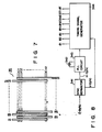
- the image display apparatus comprises: first A/D converter 31a for converting signal Y supplied from circuit 23 of Fig. 5 into, for example, four bit data D11, D12, D13, and D14; second A/D converter 31b for converting signal Y into four bit data D21, D22, D23, and D24, at a timing different from that of converter 31a; first segment driver 32a for driving even-numbered segment electrodes S2, S4,..., S288 of liquid crystal display panel 35 consisting of, for example, 112 x 288 dots, as is shown in Fig.
- Controller 34 supplies clock pulse ⁇ 1, shown in Figs. 9B and 10A, to A/D converter 31a, and supplies clock pulse ⁇ 2, whose phase is shifted 180° from that of pulse ⁇ 1, to A/D converter 31b, respectively, as sampling clocks.
- data D11 through D14 and data D21 through D24 are output having a 180° phase difference, i.e., output alternately from A/D converters 31a and 31b, respectively.
- Panel 35 shown in Fig. 7 has electrodes consisting of, for example, 112 x 288 dots.
- odd-numbered electrodes S1, S3,..., S287 are extracted from the upper side of the panel and even-numbered electrodes S2, S4,..., S288 are extracted from the lower side thereof.
- Signal C-Sync output from circuit 23 is input to sync separator 341 and therein is separated into vertical sync signal V-Sync and horizontal sync signal H-Sync.
- Signal H-Sync is input to PLL circuit 343, which includes oscillator 342.
- PLL circuit 343 locks a phase of an oscillation frequency signal from oscillator 342 to that of signal H-Sync, and supplies a stable frequency signal to timing signal generator 344.
- Generator 344 divides the input frequency signal, as required, and generates and outputs various timing signals.
- Pulses ⁇ 1 and ⁇ 2 shown in Figs. 9B and 9C, respectively, are clock pulses whose phases are shifted 180° from each other. Pulse ⁇ 2 is supplied to A/D converter 31a, as a sampling clock, and pulse ⁇ 1 is supplied thereto, as an output clock, respectively. Pulse ⁇ 1 is supplied to A/D converter 31b, as a sampling clock, and pulse ⁇ 2 is supplied thereto, as an output clock, respectively.
- Figs. 9B and 9C show only small numbers of pulses ⁇ 1 and ⁇ 2 produced during a period of one H-sync signal.
- pulses ⁇ 1 and ⁇ 2 are actually output by the number half that of a sampling number during the period of one H-sync signal (144 in this embodiment).
- Pulse ⁇ 2 is also supplied to drivers 32a and 32b.
- STI represents a shift data signal supplied to drivers 32a and 32b.
- Data D11 through D14 and data D21 through D24 are fetched while signal STI is shifted by pulse ⁇ 2.
- the data is latched in buffers (not shown) of drivers 32a and 32b by clock pulse ⁇ n1, shown in Fig. 9D.
- gradation signals are generated by gradation signal generation clock pulse ⁇ c, shown in Fig. 9K.
- the gradation signals are supplied from driver 32a to electrodes S2 through S288, and supplied from driver 32b to electrodes S1 through S287, respectively. Arrangements and operations of drivers 32a and 32b are described in detail in U.S. Serial No. 907,679.
- Dout shown in Fig. 9F, represents a shift data signal to be supplied to driver 33. Signals Dout are output one by one in units of fields, sequentially shifted by timing signal ⁇ n2, shown in Fig. 9E, and then supplied to electrodes C1 through C112.
- Symbol ⁇ f shown in Fig. 9F, represents a frame signal for AC-driving a liquid crystal. Signal ⁇ f is inverted in units of fields.
- signal ⁇ f is at level "1" in a field shown in Fig. 9J and goes to level "0" in the next field.
- the level of a signal to be supplied to the segment and common electrodes is inverted in accordance with signal ⁇ f, thereby AC-driving the liquid crystal.
- A/D converter 31a samples signal Y by pulse ⁇ 2.
- A/D converter 31a converts signal Y into data D11 through D14, and outputs them to driver 32a by pulse ⁇ 1.
- A/D converter 31b samples signal Y by pulse ⁇ 1, converts signal Y into data D21 to D24, and outputs them to driver 32b by pulse ⁇ 2, as shown in Fig. 10. Therefore, driver 32a sequentially reads data D11 through D14 supplied from A/D converter 31a.
- driver 32a drives even-numbered electrodes S2, S4,..., S288 of panel 35 in accordance with data contents.
- Driver 32b sequentially reads data D21 through D24 supplied from A/D converter 31b in a phase shifted 180° from that of driver 32a.
- driver 32b drives odd-numbered electrode S1, S3,..., S287 of panel 35 in accordance with data contents.
- the odd-numbered electrodes whose terminals are extracted upward from panel 35 and the even-numbered electrodes whose terminals are extracted downward therefrom are simultaneously driven by drivers 32a and 32b.
- Driver 33 starts scanning of the common electrodes in synchronism with signal Dout synchronized with the vertical sync signal and sequentially drives electrodes C1 through C112 selectively at predetermined timings. By driving the electrodes by drivers 32a, 32b, and 33, an image corresponding to signal Y is displayed on panel 35.
- A/D converters 31a and 31b alternately A/D-convert the video signals supplied from the video amplifier and output them to drivers 32a and 32b, an operation frequency can be reduced half that required when video signals are sequentially A/D-converted by a single A/D converter.
- driver 32a drives the even-numbered segment electrodes of panel 35
- driver 32b drives the odd-numbered segment electrodes thereof, respectively.
- the odd-numbered electrodes may be driven by driver 32a
- the even-numbered electrodes may be driven by driver 32b.
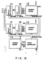
- Fig. 11 is a block diagram of a receiver of a color television circuit.
- a radio wave received by antenna 41 is tuned by tuner 42, and luminance signal Y, color television signal C, and composite sync signal C-Sync are output through television linear circuit 43 which includes an intermediate frequency amplifier, a video detector, and a video amplifier.
- Signals Y and C are input to chroma circuit 44, and primary color signals R, G, and B are output therefrom.
- An audio signal is detected and amplified by audio circuit 45 which includes an audio detector, an audio amplifier, and the like, and a sound is generated from loudspeaker 46.
- Fig. 12 is a block diagram of an image display apparatus for displaying a television image received by the above color television receiver.
- signals R, G, and B supplied from circuit 44 are input to first analog multiplexer 51a and second analog multiplexer 51b.
- Multiplexer 51a time-divisionally mixes signals R, G, and B in a predetermined order and outputs mixed signal AD1 to first A/D converter 52a.
- Multiplexer 51b time-divisionally mixes signals R, G, and B at a timing different from that of multiplexer 51a and outputs mixed signal AD2 to second A/D converter 52b.
- A/D converters 52a and 52b convert signals AD1 and AD2 into, e.g, four bit data D11 through D14 and D21 through D24 at different timings and output them to first and second segment drivers 53a and 53b, respectively.
- Driver 53a drives even-numbered segment electrodes G1, R2,..., B144 extending downward from color liquid crystal panel 56 of, e.g., 112 x 144 x 3 dots as shown in Fig. 13 in accordance with data D11 through D14 from A/D converter 52a.
- Driver 53b drives odd-numbered segment electrodes R1, B1,..., G144 extending upward from panel 56 in accordance with data D21 through D24 from A/D converter 52b.
- panel 56 shown in Fig. 13 has electrodes of, e.g., 112 x 144 x 3 dots. In panel 56, odd-numbered electrodes R1, B1,..., G144 are extracted upward, and even-numbered electrodes G1, R2,..., B144 are extracted downward.
- Common electrodes C1 through C112 of panel 56 are sequentially and selectively driven by common driver 54. Operation timings between multiplexers 51a and 51b, A/D converters 52a and 52b, and drivers 53a, 53b, and 54 are controlled by timing controller 55.
- controller 55 An arrangement of controller 55 is shown in Fig. 14. A detailed description of controller 55 will be omitted since it has substantially the same arrangement as that of timing controller 34 of the first embodiment shown in Fig. 8 except that timing signal generator 554 generates switch signals AN1 through AN6. Signals AN1 through AN6 are supplied to multiplexers 51a and 51b, and their timings are shown in Figs. 16D through 16I.
- Multiplexers 51a and 51b will be described in detail with reference to Fig. 15.
- Multiplexer 51a consists of analog switches SW1, SW2, and SW3. Signals G, R, and B are input to switches SW1, SW2, and SW3, respectively. Switches SW1 through SW3 are controlled by signals AN1 through AN3, respectively. Signals received from switches SW1 through SW3 are mixed with each other and supplied to A/D converter 52a as mixed signal AD1. Signals AN1 through AN3 are sequentially output from controller 55 with a phase difference of 120° as shown in Figs. 16D through 16F.
- Multiplexer 51b consists of analog switches SW4, SW5, and SW6. Signals B, G, and R are input to switches SW4, SW5, and SW6, respectively. Switches SW4 through SW6 are controlled by signals AN4 through AN6, respectively. Signals received from switches SW4 through SW6 are mixed with each other and supplied to A/D converter 52b as mixed signal AD2. Signals AN4 through AN6 are output from controller 55 with a phase difference of 120° with each other and a delay of 60° with respect to signals AN1 through AN3, as shown in Figs. 16G through 161.
- multiplexers 51a and 51b time-divisionally mix signals R, G, and B and output mixed signals AD1 and AD2 to A/D converters 52a and 52b, respectively. That is, when switches SW1 through SW3 are sequentially selected and turned on by signals AN1 through AN3, multiplexer 51a selectively mixes the color signals in the order of G1 ⁇ R2 ⁇ B2 ⁇ G3... as shown in Fig. 16J and outputs signal AD1 to A/D converter 52a.
- A/D converter 52a samples signal AD1, converts it into four bit data D11 through D14, and outputs them to driver 53a.
- Driver 53a sequentially reads data D11 through D14 supplied from A/D converter 52a. When data of one line are transferred, driver 53a drives even-numbered electrodes G1, R2, B2,..., R144, and B144 extending downward from panel 56 in accordance with data contents.
- multiplexer 51b selectively mixes the color signals in the order of R1 ⁇ B1 ⁇ G2 ⁇ R3... as shown in Fig. 16K and outputs signal AD2 to A/D converter 52b.
- A/D converter 52b samples signal AD2, converts it into four bit data D21 through D24, and outputs them to driver 53b.
- Driver 53b sequentially reads data D21 through D24 supplied from A/D converter 52b. When data of one line are transferred, driver 53b drives odd-numbered electrodes R1, B1, G2,..., and G144 extending upward from panel 56 in accordance with data contents.
- the odd-numbered electrodes extracted upward from panel 56 and the even-numbered electrodes extracted downward therefrom are simultaneously driven by drivers 53a and 53b. Therefore, all of electrodes R1, G1, B1, R2, G2, B3,..., R144, G144, and B144 of one line can be driven at the same time.
- Driver 54 starts scanning the common electrodes in synchronism with the vertical sync signal and sequentially drives electrodes C1 through C112 selectively at predetermined timings. By driving the electrodes by drivers 53a, 53b, and 54, a color image corresponding to signals R, G, and B is displayed on panel 56.
Claims (12)
- Bildanzeigevorrichtung, ein Flüssigkristall-Anzeigefeld (35; 56) enthaltend, bei dem Segmentelektroden und gemeinsame Elektroden in Matrixart angeordnet sind und das man erhält durch Extrahieren der ungeradzahligen Segmentelektroden und der geradzahligen Segmentelektroden aus verschiedenen Seiten, die sich gegenüberstehen; A/D-Wandlereinrichtung (31a, 31b; 52a, 52b) zum A/D-wandeln eines Videosignals; Segmenttreiber (32a, 32b; 53a, 53b) für den Betrieb der Segmentelektroden, in Übereinstimmung mit einem Ausgangssignal der A/D-Wandlervorrichtung; und ein gemeinsamer Treiber (33, 54) für den Betrieb der gemeinsame Elektroden, dadurch gekennzeichnet daß,
die A/D-Wandlereinrichtung einen ersten A/D-Wandler zum Umwandlen des Videosignals in digitale Daten bei einem bestimmten Phasenzeitpunkt und einen zweiten A/D-Wandler (31b; 52b) umfaßt, zum Umwandlen des Videosignals in digitale Daten bei einem Zeitpunkt, bei dem sich die Phase von der des ersten A/D-Wandlers (31a; 52a) unterscheidet, wobei jeder der ersten und zweiten A/D-Wandler (31a; 52a, 31b; 52b) derart eingerichtet ist, daß sie bei einer Abtastfrequenz (fs), die im wesentlichen n/2T entspricht arbeitet, wobei n die Anzahl der Bildpunkte in einer horizontalen Zeile darstellt und T die wirksame Periode einer Abtastzeile ist;
und daß die Segmenttreiber einen ersten Segmenttreiber (32a; 53a) umfassen für den Betrieb der ungeradzahligen Segmentelektroden (51, 53 ...) des Flüssigkeits-Anzeigefeldes (35; 56) in Übereinstimmung mit einem Ausgangssignal des ersten A/D-Wandlers (31a; 52a); und einen zweiten Segmenttreiber (32b; 53b) für den Betrieb der geradzahligen Segmentelektroden (52, 54 ...) des Flüssigkristall-Anzeigefelds (35; 56) in Übereinstimmung mit einem Ausgangssignal des zweiten A/D-Wandlers (31b; 52b). - Bildanzeigevorrichtung nach Anspruch 1, wobei das Flüssigkristall-Anzeigefeld (56) ein farbiges Flüssigkristall-Anzeigefeld ist;
es sind erste und zweite Analogmultiplexer (51a, 51b) für das Zeitteilmischen von Primärfarbsignalen von Rot (R), Grün (G) und Blau (B) vorgesehen, welche auf dem farbigen Flüssigkristallfeld (56) in einer Reihenfolge entsprechend der Segmentelektroden, die aus der jeweils oberen und der unteren Seite des farbigen Flüssigkristall-Anzeigefelds (56) extrahiert werden, angezeigt werden sollen;
und jede Segmentelektrode wird immer mit nur einer der R-, G- und B- Primärfarbsignale in Verbindung gebracht. - Eine Vorrichtung nach Anspruch 2, bei der jede Segmentelektrode in einer Reihenfolge einer der Kombinationen entsprechend R, G, B angeordnet ist.
- Eine Vorrichtung nach Anspruch 1 oder 2, bei der die ungeradzahlige Segmentelektroden (S₁, S₃,...) und die geradzahligen Segmentelektroden (S₂, S₄,...) so angeordnet sind, daß sie sich in entgegengesetzte Richtungen erstrecken.
- Eine Vorrichtung nach Anspruch 2, bei der weiterhin eine Fernsehschaltung (23) vorgesehen ist, und bei der die ersten und zweiten A/D-Wandler (52a, 52b) so angeordnet sind, daß sie Primärfarbsignale, die von der Fernsehschaltung (23) abgegeben werden A/D-wandeln.
- Eine Vorrichtung nach Anspruch 1 bei der weiterhin eine Fernsehschaltung (23) vorgesehen ist, und bei der die ersten und zweiten A/D-Wandler (31a; 52a, 31b; 52b) dazu eingerichtet sind, ein Helligkeitssignal, das von der Fernsehschaltung (23) abgegeben wird, A/D zu wandeln.
- Eine Vorrichtung nach Anspruch 2, bei der der erste Analogmultiplexer (51a) Einrichtungen für das abwechselnde Wählen von zwei Signalen aus R (Rot), G (Grün) und B (Blau) für einen einzelnen Bildpunkt enthält, und für das Wählen des übrigbleibenden der R-, G- und B- Signale für einen anderen einzelnen Bildpunkt.
- Eine Vorrichtung nach Anspruch 2, bei der der zweite Analogmultiplexer (51b) Einrichtungen für das abwechselnde Wählen von zwei Signalen aus den R (Rot), G (Grün) und B (Blau) Signalen für einen einzelnen Bildpunkt enthält und für das Wählen des übrigbleibenden der R-, G- und B- Signale für einen anderen einzelnen Bildpunkt.
- Eine Vorrichtung nach Anspruch 2, dadurch gekennzeichnet, daß der erste Aanalogmultiplexer (51a) dazu eingerichtet ist, um abwechselnd die Wahl von zwei aus den R- (Rot), G- (Grün) und B- (Blau) Signalen für einen einzelnen Bildpunkt zu treffen und die Wahl eines der R-, G- und B- Signale für einen einzelnen Bildpunkt auszuführen, und der zweite Analogmultiplexer (51b) dazu eingerichtet ist, abwechselnd die Wahl von zwei aus den R- (Rot), G- (Grün) und B- (Blau) Signalen für einen einzelnen Bildpunkt zu treffen und die Auswahl aus einem der R-, G-, und B- Signale für einen einzelnen Bildpunkt zu treffen, der erste Analogmultiplexer (51a) wählt zwei der R-, G- und B- Signale für einen einzelnen Bildpunkt, während der zweite Analogmultiplexer (51b) eines der übrigbleibenden R-, G- und B- Signale für einen einzelnen Bildpunkt wählt, und der erste Analogmultiplexer (51a) wählt eines der R-, G- und B- Signale für einen einzelnen Bildpunkt, während der zweite Analogmultiplexer (51b) die zwei übrigbleibenden R, G und B Signale für einen einzelnen Bildpunkt wählt.
- Eine Vorrichtung nach Anspruch 2, bei der der erste A/D-Wandler (31a; 52a) abwechselnd A/D-Wandlungen von zwei der R- (Rot), G- (Grün) und B- (Blau) Signale für einen einzelnen Bildpunkt ausführt, und A/D-Wandlungen für das übrigbleibende R- G- und B- Signal für einen einzelnen Bildpunkt ausführt.
- Eine Vorrichtung nach Anspruch 2, in der der genannte A/D-Wandler (31b; 52b) abwechselnd A/D-Wandlungen von zwei der R- (Rot), G- (Grün) und B- (Blau) Signale für einen einzelnen Bildpunkt aus führt, und A/D-Wandlungen eines der übrigbleibenden R-, G- und B- Signale für einen einzelnen Bildpunkt ausführt.
- Eine Vorrichtung nach Anspruch 2, bei der der erste A/D-Wandler (31a, 52a) dazu eingerichtet ist, abwechselnd A/D-Wandlungen von zwei der R- (Rot), G- (Grün) und B- (Blau) Signale für einen einzelnen Bildpunkt auszuführen, und A/D-Wandlungen eines der übrigbleibenden R-, G- und B- Signale für den einzelnen Bildpunkt ausführen, der zweite A/D-Wandler (31b, 52b) ist dazu eingerichtet ist, abwechselnd A/D-Wandlungen von zwei der R- (Rot), G- (Grün) und B- (Blau) Signale für einen einzelnen Bildpunkt auszuführen, und A/D-Wandlungen eines der übrigbleibenden R-, G- und B- Signale für den einzelnen Bildpunkt auszuführen, der erste A/D-Wandler (31a, 52a) zwei der R-, G- und B- Signale für einen einzelnen Bildpunkt A/D wandelt, während der zweite A/D-Wandler (31b, 52b) das übrigbleibende der R-, G- und B- Signale für den einzelnen Bildpunkt A/D-wandelt, und der erste A/D-Wandler (31a, 52a) eines der R-, G- und B- Signale für einen einzelnen Bildpunkt A/D-wandelt, während der zweite A/D-Wandler (31b, 52b) die übrigbleibenden zwei R-, G- und B- Signale für den einzelnen Bildpunkt A/D-wandelt.
Applications Claiming Priority (4)
| Application Number | Priority Date | Filing Date | Title |
|---|---|---|---|
| JP160049/86U | 1986-10-21 | ||
| JP1986160049U JPH0641270Y2 (ja) | 1986-10-21 | 1986-10-21 | 画像表示装置 |
| JP16325686U JPS6368277U (de) | 1986-10-24 | 1986-10-24 | |
| JP163256/86U | 1986-10-24 |
Publications (3)
| Publication Number | Publication Date |
|---|---|
| EP0264918A2 EP0264918A2 (de) | 1988-04-27 |
| EP0264918A3 EP0264918A3 (en) | 1989-01-11 |
| EP0264918B1 true EP0264918B1 (de) | 1991-08-28 |
Family
ID=26486654
Family Applications (1)
| Application Number | Title | Priority Date | Filing Date |
|---|---|---|---|
| EP87115354A Expired - Lifetime EP0264918B1 (de) | 1986-10-21 | 1987-10-20 | Bildanzeigevorrichtung |
Country Status (4)
| Country | Link |
|---|---|
| US (1) | US4878047A (de) |
| EP (1) | EP0264918B1 (de) |
| KR (2) | KR910003142B1 (de) |
| DE (1) | DE3772509D1 (de) |
Families Citing this family (4)
| Publication number | Priority date | Publication date | Assignee | Title |
|---|---|---|---|---|
| JPH02168296A (ja) * | 1988-12-22 | 1990-06-28 | Mitsubishi Electric Corp | 液晶表示装置 |
| US5168270A (en) * | 1990-05-16 | 1992-12-01 | Nippon Telegraph And Telephone Corporation | Liquid crystal display device capable of selecting display definition modes, and driving method therefor |
| KR100229380B1 (ko) * | 1997-05-17 | 1999-11-01 | 구자홍 | 디지탈방식의 액정표시판넬 구동회로 |
| JPH1138382A (ja) * | 1997-07-15 | 1999-02-12 | Alps Electric Co Ltd | 液晶表示装置 |
Family Cites Families (13)
| Publication number | Priority date | Publication date | Assignee | Title |
|---|---|---|---|---|
| US3862360A (en) * | 1973-04-18 | 1975-01-21 | Hughes Aircraft Co | Liquid crystal display system with integrated signal storage circuitry |
| DE3019832C2 (de) * | 1979-05-28 | 1986-10-16 | Kabushiki Kaisha Suwa Seikosha, Shinjuku, Tokio/Tokyo | Treiberschaltung für eine Flüssigkristallanzeigematrix |
| GB2081018B (en) * | 1980-07-31 | 1985-06-26 | Suwa Seikosha Kk | Active matrix assembly for display device |
| DE3268313D1 (en) * | 1981-10-29 | 1986-02-13 | Toshiba Kk | Drive circuit for display panel having display elements disposed in matrix form |
| JPS58142686A (ja) * | 1982-02-18 | 1983-08-24 | Casio Comput Co Ltd | 液晶テレビジヨン受像機 |
| JPS5961818A (ja) * | 1982-10-01 | 1984-04-09 | Seiko Epson Corp | 液晶表示装置 |
| JPH07118794B2 (ja) * | 1983-03-16 | 1995-12-18 | シチズン時計株式会社 | 表示装置 |
| JPS59176985A (ja) * | 1983-03-26 | 1984-10-06 | Citizen Watch Co Ltd | 液晶テレビ受信装置 |
| JPH0628423B2 (ja) * | 1983-12-02 | 1994-04-13 | カシオ計算機株式会社 | 画像表示装置 |
| JPS60120677A (ja) * | 1983-12-02 | 1985-06-28 | Casio Comput Co Ltd | 画像表示装置 |
| JPS6188676A (ja) * | 1984-10-05 | 1986-05-06 | Citizen Watch Co Ltd | 液晶テレビ装置 |
| US4745485A (en) * | 1985-01-28 | 1988-05-17 | Sanyo Electric Co., Ltd | Picture display device |
| JPS62271570A (ja) * | 1987-02-06 | 1987-11-25 | Seiko Epson Corp | 液晶表示装置のad変換方式 |
-
1987
- 1987-10-16 KR KR1019870011517D patent/KR910003142B1/ko active
- 1987-10-16 US US07/111,686 patent/US4878047A/en not_active Expired - Lifetime
- 1987-10-16 KR KR870011517A patent/KR880005792A/ko not_active IP Right Cessation
- 1987-10-20 EP EP87115354A patent/EP0264918B1/de not_active Expired - Lifetime
- 1987-10-20 DE DE8787115354T patent/DE3772509D1/de not_active Expired - Fee Related
Also Published As
| Publication number | Publication date |
|---|---|
| KR880005792A (ko) | 1988-06-30 |
| KR910003142B1 (ko) | 1991-05-20 |
| DE3772509D1 (de) | 1991-10-02 |
| EP0264918A3 (en) | 1989-01-11 |
| EP0264918A2 (de) | 1988-04-27 |
| US4878047A (en) | 1989-10-31 |
Similar Documents
| Publication | Publication Date | Title |
|---|---|---|
| EP0382567B1 (de) | Flüssigkristallanzeigeeinheit und Steuerverfahren dafür | |
| EP1376519B1 (de) | Bildanzeigevorrichtung und Treiberschaltung mit Einstellung der Auflösung | |
| US4642694A (en) | Television video signal A/D converter | |
| JPH088674B2 (ja) | 表示装置 | |
| EP0264918B1 (de) | Bildanzeigevorrichtung | |
| US20080122811A1 (en) | Driver Monolithic Liquid Crystal Panel Driver Circuit And Liquid Crystal Display Having Same | |
| US5189407A (en) | Multi-color display system | |
| US5754244A (en) | Image display apparatus with line number conversion | |
| US6657640B2 (en) | Image display apparatus | |
| JP2564985B2 (ja) | カラー画像表示装置 | |
| JPH07168542A (ja) | 液晶表示装置 | |
| JP2564847B2 (ja) | カラー画像表示回路 | |
| JP3211320B2 (ja) | 液晶駆動方式 | |
| JPH11338403A (ja) | 表示装置 | |
| JPH07129125A (ja) | 画素配列表示装置 | |
| JPH0744670B2 (ja) | 液晶表示装置 | |
| JPH0573001A (ja) | 液晶表示装置の駆動方法 | |
| JPH0641270Y2 (ja) | 画像表示装置 | |
| JP2615449B2 (ja) | 信号切換回路 | |
| JP2677567B2 (ja) | 液晶表示装置 | |
| JPH0375692A (ja) | マトリクス型ディスプレイの駆動回路 | |
| JPH01145693A (ja) | マトリクス型ディスプレイのデータドライバ | |
| JPS6175322A (ja) | 液晶階調表示方法 | |
| JPS60120677A (ja) | 画像表示装置 | |
| JPH06180562A (ja) | 液晶表示装置 |
Legal Events
| Date | Code | Title | Description |
|---|---|---|---|
| PUAI | Public reference made under article 153(3) epc to a published international application that has entered the european phase |
Free format text: ORIGINAL CODE: 0009012 |
|
| 17P | Request for examination filed |
Effective date: 19871020 |
|
| AK | Designated contracting states |
Kind code of ref document: A2 Designated state(s): DE FR GB |
|
| PUAL | Search report despatched |
Free format text: ORIGINAL CODE: 0009013 |
|
| AK | Designated contracting states |
Kind code of ref document: A3 Designated state(s): DE FR GB |
|
| 17Q | First examination report despatched |
Effective date: 19900418 |
|
| GRAA | (expected) grant |
Free format text: ORIGINAL CODE: 0009210 |
|
| AK | Designated contracting states |
Kind code of ref document: B1 Designated state(s): DE FR GB |
|
| REF | Corresponds to: |
Ref document number: 3772509 Country of ref document: DE Date of ref document: 19911002 |
|
| ET | Fr: translation filed | ||
| PLBE | No opposition filed within time limit |
Free format text: ORIGINAL CODE: 0009261 |
|
| STAA | Information on the status of an ep patent application or granted ep patent |
Free format text: STATUS: NO OPPOSITION FILED WITHIN TIME LIMIT |
|
| 26N | No opposition filed | ||
| PGFP | Annual fee paid to national office [announced via postgrant information from national office to epo] |
Ref country code: FR Payment date: 20011010 Year of fee payment: 15 |
|
| PGFP | Annual fee paid to national office [announced via postgrant information from national office to epo] |
Ref country code: GB Payment date: 20011024 Year of fee payment: 15 |
|
| PGFP | Annual fee paid to national office [announced via postgrant information from national office to epo] |
Ref country code: DE Payment date: 20011105 Year of fee payment: 15 |
|
| REG | Reference to a national code |
Ref country code: GB Ref legal event code: IF02 |
|
| PG25 | Lapsed in a contracting state [announced via postgrant information from national office to epo] |
Ref country code: GB Free format text: LAPSE BECAUSE OF NON-PAYMENT OF DUE FEES Effective date: 20021020 |
|
| PG25 | Lapsed in a contracting state [announced via postgrant information from national office to epo] |
Ref country code: DE Free format text: LAPSE BECAUSE OF NON-PAYMENT OF DUE FEES Effective date: 20030501 |
|
| GBPC | Gb: european patent ceased through non-payment of renewal fee |
Effective date: 20021020 |
|
| PG25 | Lapsed in a contracting state [announced via postgrant information from national office to epo] |
Ref country code: FR Free format text: LAPSE BECAUSE OF NON-PAYMENT OF DUE FEES Effective date: 20030630 |
|
| REG | Reference to a national code |
Ref country code: FR Ref legal event code: ST |